10-14
Exploded view 5DTC mechanic - for orientation only
Page 1: ... Board 6 ECO6 Tuner Board System Non Cenelec 7A System Cenelec 7B Mains Board 8 Combi Regulator Boards 9 5DTC Module Basic Version 10 Set Mechanical Exploded view parts list 11 Copyright 2003 Philips Consumer Electronics B V Eindhoven The Netherlands All rights reserved No part of this publication may be reproduced stored in a retrieval system or transmitted in any form or by any means electronic ...
Page 2: ...CUITBOARDS 22 25 30 37 Aux in CDR in x x x x Line Out Surround Out Subwoofer Out Digital Out Digital in Matrix Surround CD Text Dolby B RDS x x News x x Dolby Pro Logic DPL Incredible Surround Karaoke Features Voltage Selector ECO Power Standby Clock Display Off x x ECO6 Tuner Board Systems Non Cenelec x x ECO6 Tuner Board Systems Cenelec x x USB PC LINK x x x x VERSION VARIATIONS Type Versions MC...
Page 3: ...rejection 28dB Distortion at RF 50mV m 80 5 AMPLIFIER Output power 6Ω 1kHz 10 THD L R 2 x 50W RMS Output power 6Ω 60Hz 12 5kHz 10 THD L R 2 x 45W FTC 37 Frequency response within 3dB 50Hz 16kHz MAX Sound ON OFF Digital Sound Control DSC Pop Jazz Optimal Rock Virtual Environment Control VEC Cyber Hall Concert Cinema Off Input sensitivity Aux in at 1kHz 500mV 3dB at 600Ω CDR in at 1kHz 1V 3dB at 600...
Page 4: ...15kHz e g 7122 707 48001 LF Voltmeter e g PM2534 DUT S N and distortion meter e g Sound Technology ST1700B Frame aerial e g 7122 707 89001 Tuner AM MW LW To avoid atmospheric interference all AM measurements have to be carried out in a Faraday s cage Use a bandpass filter or at least a high pass filter with 250Hz to eliminate hum 50Hz 100Hz RF Generator e g PM5326 Ri 50Ω Bandpass 250Hz 15kHz e g 7...
Page 5: ...822 397 30155 SBC429 Audio Signals disc 4822 397 30184 Dolby Pro logic Test Disc 4822 395 10216 ESD Equipment Anti static table mat large 1200x650x1 25mm 4822 466 10953 Anti static table mat small 600x650x1 25mm 4822 466 10958 Anti static wristband 4822 395 10223 Connector box 1MΩ 4822 320 11307 Extension cable to connect wristband to conn box 4822 320 11305 Connecting cable to connect table mat t...
Page 6: ...servazione della più grande cauzione alla loro manipolazione Durante le riparazioni occorre quindi essere collegato allo stesso potenziale che quello della massa dell apparecchio tramite un braccialetto a resistenza Assicurarsi che i componenti e anche gli utensili con quali si lavora siano anche a questo potenziale Pour votre sécurité ces documents doivent être utilisés par des spécia listes agré...
Page 7: ...ase the fixation of the Combi Board pos 1102 1003 to Bracket Combi pos 252 by releasing the 2 catches C1 see Figure 5 and pulling the Combi Board outwards as shown in Figure 6 3 Uncatch 2 catches C2 see Figure 5 on the left right sides of the Cabinet Front pos 101 and slides the Front Panel assembly out towards the front Detaching the Front Panel assembly from the Bottom Rear assembly 4 To remove ...
Page 8: ...remove the USB PC LINK Board pos 1106 Dismantling of the Rear Panel assembly 1 Loosen 3 screws H and 2 catches C3 see Figure 9 to remove the Tuner Board assembly 2 Loosen 1 screw K see Figure 9 to free the Mains Socket Board pos 1102 1001B 3 Loosen 4 screws J and 2 catches C4 see Figure 9 to remove the Cabinet Rear pos 256 by sliding it out towards the rear see Figuer 10 Note Tuner Board assembly ...
Page 9: ...n that area This will not affect the performance of the rest of the set Note The flex cables are very fragile care should be taken not to damage them during repair After repair be very sure that the flex cables are inserted properly intotheflexsocketsbeforeencasing otherwisefaults may occurs Service position B Service position C Service position A DISMANTLING INSTRUCTIONS ...
Page 10: ...tivities can be carried out SERVICE PLAY MODE For MC 500 only DTC works as in normal operation In case of failures error codes according to Table 2 will be displayed Display shows 5DTC Vnn Version of 5DTC control software nn Version Number Various other Tests Activated with ACTION TEST Q EEPROM FORMAT TEST Load default data Display shows NEW for 1 second Caution All presets from the customer will ...
Page 11: ...ILTER C1 EEPROM ECO POWER F2 RDS ATTEN AM 80 MOD INCREDIBLE 1 90V 67dBA FM 67 5 kHz LEFT RIGHT LEFT RIGHT 125mV 5V6_ECO I2C DATA 33V 76dBA M HEADPHONE CHOKE 12V_A F2x SELECTOR HP_OUT FRONT PWDN TRAFO SOURCE SELECTOR ATTN 9V AUX CDR IR EYE ADC 5V6 F2x NOT USED FOR 37 I2C CLK A2 3 0dB D F1 LOW_POWER_CONTROL 5V_CD CONTROL A 16dB 5DTC POWER SUPPLY Rin 3k D 250mV ZZ dB VOLUME CONTROL ECO6 AMPLIFIER 2 5...
Page 12: ...08 TRAFO 1 LEGEND 8200 1P 180 mm 1P 100 mm 2P 260mm TRAFO N L 1204 EHS EH SIDE ENTRY 9P 120mm 1 1 1102 9P 220mm 8002 FCT 1400 EHT 1203 8P 280mm AD Fold EHT 1400 1 FCS 1702 USB 1106 8P 100mm BD 8006 7P 180mm AD 1105 COMBI PIN TYPE 1 1103 ECO6 1101 1 1 TO BOTTOM PLATE 4P 120mm AD 8007 FCT 1022 STABILISER FCS 1301 8009 SUPPLY MAINS 1 FCS 1703 TO BOTTOM PLATE 1 FCT 1120 LOUDSPEAKER 1307 1001 B 2P 100m...
Page 13: ...d col Dp 8G a h j p k b f m g c e r n d FTD DISPLAY PIN CONNECTION 1G 10G 10G 2G 9G 2G 9G S6 S5 S4 S3 S2 S1 S7 S7 a d j k b h f p n c r g m e S1 S2 S3 S4 S5 S6 S10 S9 S8 S7 S6 S5 S4 S3 S2 S1 9G 1G 10G 2G 3G 4G 5G 6G 8G 7G col Dp B4 B3 B2 B1 B6 B5 B8 B9 B7 B4 B3 B2 B1 B6 B5 B8 B9 B7 FRONT BOARD TABLE OF CONTENTS FTD Display Pin Connection 6 1 Front Board Component layout 6 2 Front Board Chip layout...
Page 14: ...embly drawing shows a summary of all possible versions For components used in a specific version see schematic diagram and respective parts list 3139 113 3501 pt2 dd wk0251 FRONT BOARD COMPONENT LAYOUT 6 2 6 2 ...
Page 15: ...assembly drawing shows a summary of all possible versions For components used in a specific version see schematic diagram and respective parts list 3139 113 3501 pt2 dd wk0251 FRONT BOARD CHIP LAYOUT 6 3 6 3 ...
Page 16: ... 47p 2445 47p 2440 D 100p 2402 100K 3413 1M 3439 2479 22p 22u 2461 D 50V 100n 2483 VSS 4 7 WC_ 3503 1K 1K 3515 1K 3513 100p 2400 470R 3475 3505 1K D 100R 3469 1K 3472 680K 3404 47p 2444 3537 9412 4K7 CD 1N4148 6408 6402 1N4148 BC847B 7404 2K7 3420 1K 3516 100R 3466 1K 3522 D 1K 3462 3510 1K 1K 3498 1K 3500 10K 3542 1K 3502 3487 1K 10K 3418 1K 3507 3481 1K TU 1K 3524 1K8 3423 1K 3489 220K 3424 1K 3...
Page 17: ...303 1315 1K8 3343 5401 4u7 820R 820R 820R 820R 820R 820R 820R 820R 820R 820R 820R 820R 3304 2473 100n USB 2K7 3344 7406 BC857B 2307 ADC 6301 100p 2K7 3323 3345 150R 2K7 3335 ADC 3313 3301 47K 5300 2u2 6302 1301 FE ST VK N 1 1306 10K 3528 100p 2310 1307 4407 D D 3346 10K 100n 2306 1328 560R 3340 4404 820R 3300 560R 3330 1310 1304 5302 2u2 6305 3310 3307 820R 3328 3326 1320 270R 3309 1N4148 6300 HP ...
Page 18: ... 50V 4u7 2429 3543 1K 100n FTD 2478 470R 3453 100n 2464 220R 3429 47p 2448 D I2C 470R 3450 2453 47p 2482 100n 220R 3449 9413 3432 10R 47p 2450 470R 3452 10K 3440 3 4 5 6 7 8 9 47p 1402 FE ST VK N 1 2 10K 3447 CD 16V 47u 2425 FTD 4408 FE ST VK N 1 10 11 12 13 14 15 16 17 18 19 2 3 4 2432 4u7 5409 100p 1K 3444 2477 220p 2476 220p 220p 2475 220p 2474 100n 2472 D 10p 2451 4409 10p 2447 220R 3448 D TU ...
Page 19: ...bly drawing shows a summary of all possible versions For components used in a specific version see schematic diagram and respective parts list 3139 113 3501 pt2 dd wk0251 6 7 6 7 CDC KEY BOARD CIRCUIT DIAGRAM CDC KEY BOARD COMPONENT LAYOUT CDC KEY BOARD CHIP LAYOUT VARIANT TABLE X X X X 7409 33K 15K 15K 33K 3438 X X 3545 10K 10K 1M 2M2 2M2 3403 3534 1K8 1K8 3423 1K8 1K8 1K8 1M 680K 100K 100K 3406 ...
Page 20: ... 051 30221 220R 5 0 062W 3326 4822 116 83876 270R 5 0 5W 3328 4822 117 12968 820R 5 0 62W 3334 4822 116 52283 4k7 5 0 5W 3335 4822 051 30272 2k7 5 0 062W 3336 4822 051 30151 150R 5 0 062W 3337 4822 051 30221 220R 5 0 062W 3338 4822 116 83876 270R 5 0 5W 3339 4822 051 30391 390R 5 0 062W 3340 4822 051 30561 560R 5 0 062W 3341 4822 117 12968 820R 5 0 62W 3342 4822 117 11817 1k2 1 1 16W 3343 4822 117...
Page 21: ...er 0603 4433 4822 051 30008 0R Jumper 0603 4434 4822 051 30008 0R Jumper 0603 4435 4822 051 30008 0R Jumper 0603 4436 4822 051 30008 0R Jumper 0603 4437 4822 051 30008 0R Jumper 0603 4438 4822 051 30008 0R Jumper 0603 4439 4822 051 30008 0R Jumper 0603 4440 4822 051 30008 0R Jumper 0603 4441 4822 051 30008 0R Jumper 0603 4442 4822 051 30008 0R Jumper 0603 4443 4822 051 30008 0R Jumper 0603 4444 48...
Page 22: ... 6 5 43 C D 450kHz 450kHz 450kHz 20 75kHz VStabA VStabB VStabB VStabA VStabB 10 7 MHz 10 7 MHz 35 9 Vdd Vcc1 7 23 VStabA VStabB 38 34 22 Vcc2 8 ECO6 Systems 140499 LF filter RDS MPX RDS MPX stereo clock data enable Version 1120 1 8 FM Frontend AM Frontend AM FRAME AERIAL B 1103 1101 1102 A FM MPX buffer ampl 5 Discriminator 10 7 MHz Vdd Vcc1 Vcc Vcc2 AM RF AM Osc FM Osc FM RF FM IF 1 FM IF 2 AM IF...
Page 23: ...1n 3134 22K 6105 2 HN1V02H 100n 2163 T141 7KL 1K 3144 5102 3157 100K T109 470R 3153 2130 22n 220R 3105 3142 100K 3167 120R 33p 2149 2K2 3145 1132 C PAD T103 T111 2164 470n T102 2140 15p 2139 2138 2u2 82p 2133 1u 3103 8K2 T120 4p7 2154 3156 1101USA YKD21 100K 2161 100n 5119 2119 10p T142 5123 11p 2106 3172 6106 BAS216 100n 2165 5K6 3154 3155 220R 330R 2124 33K 3176 22n WRITE EN 5114 7P MUTE P0 P1 P...
Page 24: ...riginal frame antenna has to be used 2 RC network serves for damping the IF filter while adjusting the other one 4 MW has to be aligned before LW Waverange Input frequency Input Tuned to Adjust Output Scope Voltmeter FM 87 5 108MHz 65 81 74 87 5 108MHz FM MW version 9kHz grid 531 1602kHz as low as possible ECO6 System non Cenelec stage 3 120900 TUNER BOARD ECO6 Systems non Cenelec componentside vi...
Page 25: ...10 63V RDS only RESISTORS 3101 4822 051 20333 33kΩ 5 0 1W 3102 4822 117 10837 100kΩ 1 0 1W 3103 4822 051 20822 8 2kΩ 5 0 1W 3104 4822 117 13577 330Ω 1 0 1W 3105 4822 117 11503 220Ω 5 0 1W 3132 4822 051 20479 47Ω 5 0 1W 3134 4822 051 20223 22kΩ 5 0 1W 3141 4822 117 11148 56kΩ 1 0 1W 3142 4822 100 12159 TRIMPOT 100kΩ RESISTORS 3143 4822 051 20223 22kΩ 5 0 1W RDS only 3144 4822 051 10102 1kΩ 2 0 25W ...
Page 26: ... B V Stab B V Stab A V Stab B 10 7 MHz 10 7 MHz 35 9 Vdd Vcc1 7 23 V Stab A V Stab B 38 34 22 Vcc2 8 ECO6 Systems Cenelec 140499 V Loop FM AM RF AM Osc FM IF 1 FM IF 2 LF filter MPX buffer ampl RDS MPX 5 RDS MPX stereo clock data enable Version 3 1120 AM IF 1 AM IF 2 AM AFC 1 8 AM Frontend 2 AM FRAME AERIAL B 1103 1101 1102 A FM AM FM Discriminator 10 7 MHz Vdd FM Vcc1 Vcc Vcc2 MW LW AM RF AM Osc ...
Page 27: ...4 22n USA 22n USA C PAD 1131 T141 2106 11p 20p_LW 0R 4104 0R 41xx 2165 100n 1130 C PAD 10K 3180 2150 100n BZX284 C11 6107 T102 2127 220n 2169 2n2 100K 3170 1 I 3 O 2125 560p 5109 2 G 470R 3152 2108 100p 3125 10K 3153 470R 330R 3193 T103 120R 3167 100R 3195 7 8 33K 3176 8 5122 1 2 3 4 6 5123 1 2 3 4 6 7 5110 G 2 I 1 O 3 5115 1 2 3 4 6 7 8 2 3 4 6 7 8 5119 1 2135 100n 2163 LW 7104 BC337 40 2145 220p...
Page 28: ...ce Testprogram By selecting the TUNER TEST test frequencies will be stored as preset frequencies automatically AM FRAME AERIAL FM 75Ω FM FRONTEND Birdy Filter ECO6 Sys Cenelec layout stage 6 160501 1101 B5 1102 B5 1103 C5 1110 B4 1120 A4 1130 A5 1131 C5 1132 A4 2106 B4 2107 B3 2128 A3 2129 B3 2133 C1 2138 B1 2144 B1 2162 A4 2191 B4 3142 C2 5102 C4 5103 C4 5109 B3 5110 A2 5111 A3 5112 A2 5114 A2 51...
Page 29: ...98 021 38210 820Ω 5 0 06W 3132 4822 051 20479 47Ω 5 0 1W 3134 4822 051 20223 22kΩ 5 0 1W 3135 3198 021 31020 1kΩ 5 0 06W 3137 4822 051 20223 22kΩ 5 0 1W LW only 3141 4822 117 11148 56kΩ 1 0 1W 3142 4822 100 12159 TRIMPOT 100kΩ 3143 4822 051 20223 22kΩ 5 0 1W RDS only 3144 4822 051 10102 1kΩ 2 0 25W RDS only 3145 4822 117 11449 2 2kΩ 1 0 1W 3146 4822 051 20229 22Ω 5 0 1W 3150 4822 117 10833 10kΩ 1 ...
Page 30: ...t value 8 1 8 1 MAINS BOARD TABLE OF CONTENTS Brief introduction 8 1 Mains Socket Circuit diagram Component layout 8 1 Mains Board Component layout 8 2 Mains Board Chip layout 8 3 Mains Board Circuit diagram 8 4 Electrical parts list 8 5 MAINS SOCKET CIRCUIT DIAGRAM COMPONENT LAYOUT Brief introduction of the Mains Board ECO Power StandbyTransformer 5203 provides the LPS supply to control the relay...
Page 31: ...embly drawing shows a summary of all possible versions For components used in a specific version see schematic diagram and respective parts list 3139 113 3478 pt3 dd wk0247 8 2 8 2 MAINS BOARD COMPONENT LAYOUT ...
Page 32: ...assembly drawing shows a summary of all possible versions For components used in a specific version see schematic diagram and respective parts list 3139 113 3478 pt3 dd wk0247 8 3 8 3 MAINS BOARD CHIP LAYOUT ...
Page 33: ... 6223 100n 100n 2225 3226 2207 47n BC337 40 7203 470R 3222 1K5 3229 3212 2201 6226 BZX79 C39 BC847B 7205 3211 6221 1N4003 9 Low Power Supply VOLTAGE REGULATION F2 FTD T5AL RES 4K7 3228 3202 3K9 6229 1N4148 1N4148 BC817 40 7202 100K 3227 33K 3233 6227 3221 2K2 6228 1N4148 33K 7200 6202 GBU8D 100n 2204 6204 BZX79 B8V2 3231 100R 3217 47K 2229 47n 470n 2213 0u47 2208 47K 3214 3201 4K7 5 4 6 8 9 7 1 12...
Page 34: ...5 3223 4822 051 30103 10k 5 0 062W 22 25 3224 4822 117 13632 100k 1 0 62W 22 25 3225 4822 051 30475 4M7 5 0 062W 22 25 3226 4822 051 30331 330R 5 0 062W 22 25 3227 4822 117 13632 100k 1 0 62W 22 25 3228 4822 051 30472 4k7 5 0 062W 22 25 3229 4822 051 30472 4k7 5 0 062W 22 25 3230 4822 051 30333 33k 5 0 062W 22 25 3231 4822 052 10101 100R 5 0 33W 22 25 3232 4822 053 21225 2M2 5 0 5W 22 25 3233 4822...
Page 35: ...nent View seen from Copper Side 9 4 Copper Side View 9 5 Circuit diagram Source Selector part 9 6 Circuit diagram Amplifier part 9 7 Electrical parts list 9 8 Brief introduction of the Regulator Board The regulator board provides the following a 12V supply 12V_A and 12V_M derived from the A supply b 5 6V and 5V supply 5V6 and 5V_VCD derived from the A 2 supply Technical Remarks ...
Page 36: ... schematic diagram and respective parts list 3139 113 3441 pt5 This assembly drawing shows a summary of all possible versions For components used in a specific version see schematic diagram and respective parts list 3139 113 3441 pt5 9 2 9 2 REGULATOR BOARD COPPER SIDE VIEW REGULATOR BOARD COMPONENT SIDE VIEW ...
Page 37: ... GND_A 7409 BC327 25 9401 1K 3420 VCD_GND BC547B 7419 GND_M EH B 1403 3433 10K 3409 3K3 3439 1K 10K 3410 120R 3435 2413 10u 7405 BD438 6407 BZX79 B4V7 3424 470K 120R 3434 3437 100K L7805 7417 2 GND 1 IN OUT 3 180R 3432 10K 3440 GND_A VCD_GND 2322640 3418 120R 3417 7410 BD438 VCD_GND BC547B 7406 1K 3403 7407 BC547B 1N4148 6401 100n 2404 4 5 6 7 8 9 BC547B 7401 EH B 1401 1 10 11 2 3 2407 100u 100K 3...
Page 38: ...0 F8 3353 E6 3366 F5 3713 E2 5001 A9 5300 D8 5301 E8 5302 C8 5303 E8 5700 F2 6000 F3 6001 F3 6002 B2 6003 A6 6005 C2 6300 F9 6301 E8 6302 F9 6303 E8 6304 D6 6306 F6 6307 F7 6308 C6 6311 D6 6315 F7 6323 F6 6324 F6 6325 D5 6326 F3 6327 F3 6328 F5 6330 F4 6331 D5 6332 F6 7301 E8 7302 C8 7304 D8 7309 F8 9201 B8 9202 B8 9203 A7 9204 E2 9205 B7 9206 B7 9207 A8 9208 A7 9209 B6 9210 B6 9211 B6 9212 B6 921...
Page 39: ...82 C9 3083 B3 3084 A3 3085 A3 3087 B4 3088 B3 3089 A3 3091 B4 3094 A1 3095 A1 3096 E2 3097 E1 3098 A9 3099 A8 3100 A8 3101 A8 3102 A8 3105 E2 3106 E1 3107 B1 3110 B5 3111 B5 3301 E8 3302 C8 3303 E8 3304 D8 3305 F4 3306 E4 3307 E8 3308 C8 3314 E6 3318 F6 3323 F7 3326 F8 3327 F8 3328 D8 3329 F7 3331 E6 3336 E7 3337 C7 3341 F8 3342 F7 3359 F3 3360 F4 3361 F3 3362 F3 3363 F3 3364 F7 3365 F7 3367 F5 33...
Page 40: ... 2506 YKC21 3418 3424 COMBI 1 2 15p 2028 3043 2K7 3036 1001 A 1K5 470p 470p 2501 2508 3051 2K2 470R 3038 15K 3029 10K 3027 3024 15K 3022 10K 7007 BC847B 2552 22n 2551 22u 2549 100n 2056 1u 2000 10n 2025 1001 B YKC21 3418 3424 COMBI 4 5 470p MIC_DET CMOS VKK MUTE_LINE 2550 220u COAX1 SA_IN SA_IN LINE_R LINE_R LINE_R LINE_L LINE_L LINE_L LOW_PWR_CTRL 12V_A A 5V6 GND GND GND 12V_M A 2 LPC NTC POWER_D...
Page 41: ...47K 4K7 3327 2u2 I2C_DATA I2C_CLK 3314 2K2 4R7 3309 5V AMP_ON AMP_ON MUTE_SW MUTE_SW HP_DET HP_DET MUTE_HP MUTE_HP AMP_MUTE MIC_DET MIC_DET MUTE_LINE 5V CD ON MUTE_LINE 12V_A SUB_W AMP_RIGHT AMP_RIGHT AMP_LEFT AMP_LEFT CL_DET Source Selector part 50V 50V 12V_A VOL_LEFT VOL_RIGHT A Combi Amplifier Part 2001 09 24 POWER STAGE BUFFER AMPLIFIER SUPER G SWITCHES MUTE MUTE MUTE MUTE 0V 4 4V 1 3V 15 6V 0...
Page 42: ...5 50V 2032 4822 124 22651 1uF 20 50V 2033 4822 124 23052 100uF 20 16V 2038 2020 552 94427 100pF 5 50V 2045 2020 552 94427 100pF 5 50V 2046 4822 124 23052 100uF 20 16V 2048 2022 020 00734 1uF 20 50V 2056 2022 020 00734 1uF 20 50V 2058 4822 124 22651 1uF 20 50V 2060 2238 586 59812 100nF 50V 2061 2020 552 94427 100pF 5 50V 2062 2020 552 94427 100pF 5 50V 2070 2238 586 59812 100nF 50V 2080 2022 020 00...
Page 43: ...221 220R 5 0 062W 3302 4822 051 30221 220R 5 0 062W 3303 4822 051 30331 330R 5 0 062W 3304 4822 051 30331 330R 5 0 062W 3305 4822 051 30471 470R 5 0 062W 3306 4822 051 30471 470R 5 0 062W 3307 4822 051 30471 470R 5 0 062W 3308 4822 051 30471 470R 5 0 062W 3309 4822 050 24708 4R7 1 0 6W 3310 4822 050 24708 4R7 1 0 6W 3311 4822 050 24708 4R7 1 0 6W 3312 4822 050 24708 4R7 1 0 6W 3314 4822 051 30222 ...
Page 44: ...51 30008 0R Jumper 0603 4503 4822 051 30008 0R Jumper 0603 4504 4822 051 30008 0R Jumper 0603 COILS FILTERS 5005 2422 549 44608 INDFXD 0603 EMI 100MHz 1k 5006 2422 549 44608 INDFXD 0603 EMI 100MHz 1k 5262 2238 586 59812 100nF 50V 5300 4822 157 62255 Coil 18 5 Turns 5301 4822 157 62255 Coil 18 5 Turns 5302 4822 157 62255 Coil 18 5 Turns 5303 4822 157 62255 Coil 18 5 Turns 5700 4822 157 62552 Coil 2...
Page 45: ...ergency opening 10 7 Location of switches 10 8 Blockdiagram 10 9 CD BOARD Circuit Diagram 10 10 Component Layout side A 10 11 Component Layout side B 10 12 CONTROL BOARD Circuit Diagram 10 13 Component Layout 10 13 Exploded view loader 10 14 Partslist 10 15 5DTC Module Basic version Layout stage 4 ...
Page 46: ...he way as indicated in the picture below 3 MEASURE THE EYE PATTERN SIGNAL EYE PATTERN SIGNAL JITTER MEASUREMENT Measure the signal direct on resistor 3898 using an oscilloscope see also chapter 10 9 See below examples of the signal Amplitude should read at least 700mVpp using SBC444A good bad If the oscilloscope shows a signal like the bad one and or the amplitude decreases within 1minute the CD d...
Page 47: ... PROCESSOR OFFSET MEASUREMENT Each ADC input of the CD10 may have an offset too Also this offset leads together with the offsets of the CD Drive to poor playability of some CDs skipping tracks Start the Service Test Program section Focus Test using a CD RW disc Use a DC Millivoltmeter for measurement The offsets can be measured on capacitors near the signal processor See drawing below The value sh...
Page 48: ...move paperclip from flexfoil 7 Connect flexfoil to new CD drive 8 Remove ESD protection solder joint from laserunit see picture below CHARGED CAPACITORS ON THE SERVO BOARD MAY DAMAGE THE CD DRIVE ELECTRONICS WHEN CONNECTING A NEW CDM MECHANISM THAT S WHY BESIDES THE SAFETY MEASURES LIKE SWITCH OFF POWER SUPPLY ESD PROTECTION ADDITIONAL ACTIONS MUST BE TAKEN BY THE REPAIR TECHNICIAN 10 4 WARNING fi...
Page 49: ...10 5 Location of Printed Circuit Boards 5DTC Location of PCBs 2002 08 29 CD Board Control Board Motor Board MP3 Board 8051 8052 8021 MP3 Board and flexfoil cable 8051 not stuffed ...
Page 50: ...1824 1802 1801 1823 Control Board Motor Board CD Board 8021 The FFC Cables are available as sparepart 8001 3103 308 93090 FFC CABLE 16Pin 80mm BD Connection from CD Board to CD Drive 8052 3103 308 93120 FFC CABLE 8Pin 80mm BD Connection from CD Board to Control Board 8021 3103 308 93110 FFC CABLE 16Pin 60mm AD Connection from Control Board to Motor Board ...
Page 51: ...ver pos 29 forward to its endposition see picture 4 Release snap as shown in picture 5 and pull tray out To remove a CD from Play Position perform following steps 1 Open tray 1 as described before 2 Tear the tray out with speed see picture 6 The tray can be inserted aftewards without any alignment 3 Move lever pos 29 forward to its endposition see picture 4 4 Push lever pos 31 forward see picture ...
Page 52: ...10 8 Location of switches ...
Page 53: ...ram 5DTC 2002 09 05 5V 5VST 3 3V A 12V 7815 5V Vref 3servo 8V 7801 12V BLOCK DIAGRAM 5DTC 5VST 28 VREF VREF AOPAMP VREF 5VSWITCH FOCUS MOTOR RADIAL MOTOR SLEDGE MOTOR MOTOR TURNTABLE MOT1 SL RA FO 55 54 56 59 25 19 26 27 2 1 11 12 18 17 3 7802 MM1469PH TTM TTM SLEDGEB SLEDGEB RADB RADB FOCB FOCB MOT2 60 10 LD ON HF IN 64 V4 61 2 CD RW 3V CD DA 0V EQ Selection 7876 7877 7811 7879 7878 LD MON A D A ...
Page 54: ... 6 7 8 1 1824 14 15 2 3 4 5 6 7 8 9 1824 1 10 11 12 13 5V INTERFACE VERSATILE DEMOD EFM PLL DIG STAGES OUTPUT CONTROL MOTOR KILL INTERF LOOPBACK SER DATA INTERF VERSAT INTERFACE SER DATA BITSTREAM DAC TIMING INTERFACE MICROCONTROLLER PROCESSOR AUDIO PROCESSING PRE FUNCTION CONTROL SRAM ADDR INTERF EBU DET PEAK CORR ERROR PROCESSOR SUBCODE END FRONT VREF GEN ADC VSSD3 WCLI WCLK V1 V2 V3 V4 V5 VDDA1...
Page 55: ...3900 E15 3901 G6 3902 G7 3903 G7 3904 G8 3905 F8 3906 H8 3907 H7 3908 H7 3909 H9 3910 E14 3912 A11 3917 H11 3918 H4 3919 H4 3920 F7 3922 H10 3923 H9 3925 A11 3926 A11 3927 B11 3928 B11 5001 H5 5002 H11 6877 J11 7800 D11 7801 I11 7802 G2 7804 E15 7810 A B13 7810 B A13 7811 A F4 7811 B I4 7875 I11 7876 G7 7877 H8 7878 H8 7879 F3 MAPPING FOR CIRCUIT DIAGRAM 1800 D3 1810 E5 1823 D7 1824 A5 2811 B6 281...
Page 56: ...6 D4 2817 C5 2818 D4 2821 E3 2822 E3 2823 E2 2825 E2 2830 B2 2831 B4 2832 C3 2836 A6 2838 C4 2839 E5 2840 E5 2842 A4 2846 A3 2848 A4 2849 B4 2851 A3 2852 E6 2853 D6 2854 B5 2855 A4 2857 E6 2866 E4 2876 D5 2877 D5 2885 B3 2886 D3 2888 A7 3820 E5 3829 E2 3830 A4 3833 E3 3836 C3 3841 C3 3847 C3 3855 E5 3856 C3 3859 E5 3860 C3 3861 C3 3862 E6 3864 B4 3867 B4 3873 B4 3874 B4 3880 E6 3881 D6 3882 A4 389...
Page 57: ...on 2002 09 12 1800 C2 1801 E4 1802 A1 2800 A2 2801 A2 2802 B2 2803 C1 2808 A2 2810 A3 2811 D4 2812 D4 2813 E4 2814 C4 3800 C1 3802 D2 3803 D2 3804 D1 3805 D1 3806 D1 3807 D2 3808 D1 3808 D2 3809 D2 3810 B1 3811 C1 3815 C3 3816 C4 3818 D4 3819 D3 3820 D3 3821 E4 3823 C4 3824 C3 3826 A2 3827 C1 3828 C2 3829 B1 3830 B1 3831 B1 3832 E4 3833 E4 3834 E3 3835 E3 3836 E3 3837 E3 3838 E3 3839 E3 3840 E3 38...
Page 58: ...10 14 10 14 Exploded view 5DTC mechanic for orientation only ...
Page 59: ... 180pF 5 50V 2869 3198 017 34730 47nF 10 16V 2870 4822 126 13883 220pF 5 50V 2871 4822 126 13883 220pF 5 50V CAPACITORS 2872 4822 126 13883 220pF 5 50V 2873 4822 126 13883 220pF 5 50V 2874 4822 126 13883 220pF 5 50V 2875 4822 126 13883 220pF 5 50V 2876 3198 017 44740 470nF 20 10V 2877 4822 124 40433 47µF 20 25V 2878 2238 586 59812 100nF 10 50V 2879 5322 126 11578 1nF 10 63V 2880 2222 867 15339 33p...
Page 60: ...4822 051 30332 3 3kΩ 5 0 06W 3904 4822 051 30332 3 3kΩ 5 0 06W 3905 4822 051 30681 680Ω 5 0 06W 3906 4822 051 30471 470Ω 5 0 06W 3907 4822 117 12968 820Ω 5 0 06W 3908 4822 051 30222 2 2kΩ 5 0 06W 3909 4822 117 13632 100kΩ 1 0 06W 3910 4822 051 30471 470Ω 5 0 06W 3912 4822 051 30221 220Ω 5 0 06W 3916 4822 051 30471 470Ω 5 0 06W 3917 4822 117 13608 4 7Ω 5 0 06W 3918 4822 051 30103 10kΩ 5 0 06W 3919 ...
Page 61: ...51 30272 2 7kΩ 5 0 06W 3838 4822 051 30103 10kΩ 5 0 06W 3839 4822 051 30272 2 7kΩ 5 0 06W 3840 4822 051 30272 2 7kΩ 5 0 06W 3841 4822 051 30103 10kΩ 5 0 06W 3842 4822 051 30103 10kΩ 5 0 06W 3845 4822 051 20159 15Ω 5 0 1W 3850 4822 117 12706 10kΩ 1 0 06W 3851 4822 117 12706 10kΩ 1 0 06W 3852 4822 117 12706 10kΩ 1 0 06W 3853 4822 117 12706 10kΩ 1 0 06W 3854 4822 117 12706 10kΩ 1 0 06W RESISTORS 3855...
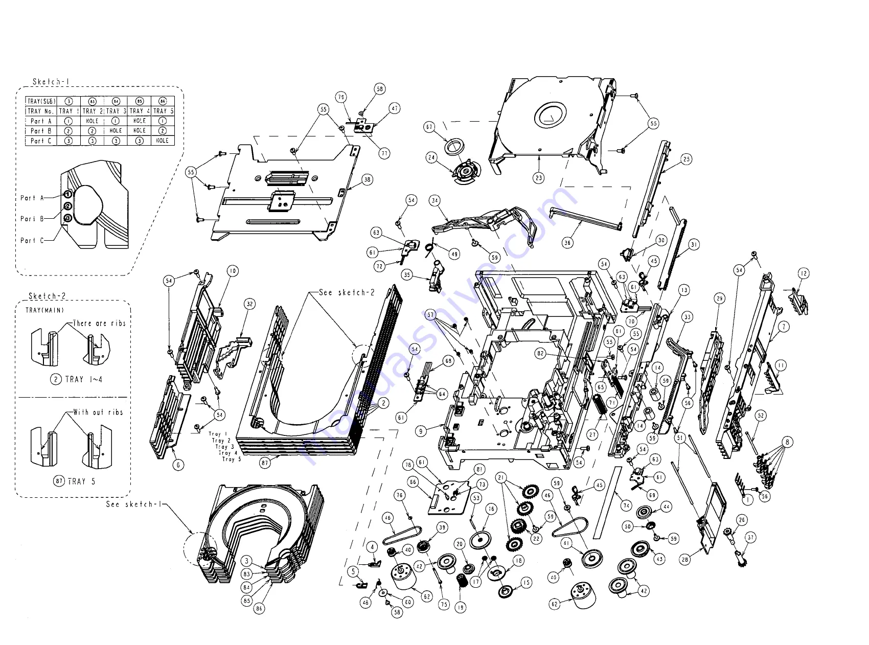
Page 62: ...Exploded_View_3139 119 35510 dd wk0251 11 1 11 1 SET MECHANICAL EXPLODED VIEW ...
Page 63: ...9 114 77242 Panel Left 22 25 30 0253 3139 114 78691 Panel Left 37 0254 3139 114 77232 Panel Right 22 25 30 0254 3139 114 78701 Panel Right 37 0255 3139 114 77631 Cover Top 22 25 30 0255 3139 114 78711 Cover Top 37 0256 3139 114 77251 Cabinet Rear 22 25 30 0256 3139 114 78721 Cabinet Rear 37 0271 3139 114 71010 Stopper Heatsink 0345 3139 119 00501 L R Loudspeaker Box 22 25 30 0345 3139 119 00491 L ...