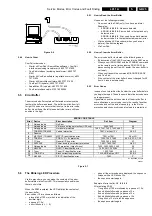
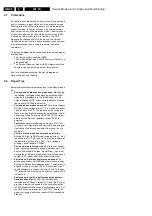
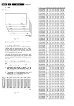
background image

Directions for Use

GB 13

L01.1A

3.

22

¸

U

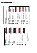
SING


THE

 T

IMER

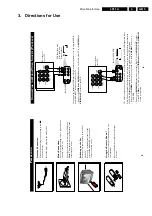
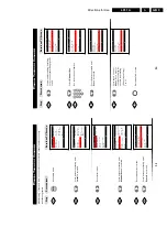
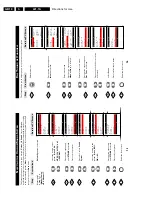
The 

Timer f

eatur

e

 allo

ws y

ou to set the timer to s

w

itch to another channel at a specified

time while y

ou ar

e watching another channel or when the 

TV is on standb

y mode

.

Note

 : F

o

r the timer to function,

 the set m

ust not be switched off.

 Once the set is s

w

itched

off, the timer is disabled.

Main

o

Picture

π

Brightness

Sound

Colour

Features

Contrast

Install

Sharpness

Colour Temp.

More...

œ

Main

o

Picture

Timer

Sound

Child Lock

Features

π

Format

Install

œ

Features

o

Timer

π

Time

Child Lock

Start Time

Format

Stop Time

Channel

Activate

Display

œ

˙

Displa

y the main men

u

 on scr

een.

Select 

F

e

atur

es

.

Enter the F

eatur

es men

u.

Enter Timer 

men

u

.

K

e

y in the cur

rent time star

ting fr

om

the hour f

o

llo

w by min

ute

.

This is the time wher

e the 

“star

t time

and 

“stop time

” will tak

e r

e

fe

rence

fr

om.

Select 

Star

t Time

.

K

e

y in the time y

o

u want the

pr

ogramme to be s

w

itched on.

Timer

o

Time

π

08:30

Start Time

Stop Time

Channel

Activate

Display

œ

˙

Timer

o

Time

Start Time

π

10:30

Stop Time

Channel

Activate

Display

œ

¸

MENU

5

1

3

2

4

6

7

9

8

0

5

1

3

2

4

6

7

9

8

0

Step

Pr

ess button

Result on 

TV Scr

een

21

A

DUSTING


THE

  TV S

OUND

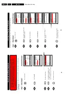
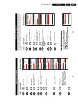
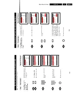
The sound men

u allo

ws y

ou to mak

e adjustments to the sound.

Displa

y the main men

u on scr

een.

Select 

Sound 

menu.

Enter 

Sound

 menu.

Select item.

Adjust lev

el or select desir

ed

setting.

Exit menu fr

om scr

een.

Main

o

Picture

π

Brightness

Sound

Colour

Features

Contrast

Install

Sharpness

Colour Temp.

More...

œ

Main

o

Picture

Treble

Sound

π

Bass

Features

Balance

Install

AVL

Incr. Surround

Ultra Bass

œ

Sound

o

Treble

p

❘❘❘❘❘❘❘❘❘❘❘

❘❘❘❘❘❘❘❘❘❘❘

0

π

Bass

Balance

AVL

Incr. Surround

Ultra Bass

œ

¸

˙

˝

˙

or

˚

or

¸

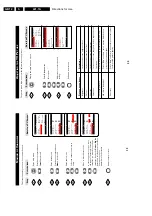
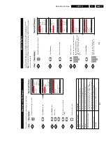
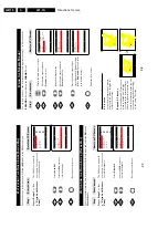
Sound men

u items

Activities

T

reble

Incr

ease or decr

ease high fr

equency le

vel.

Bass

Incr

ease or decr

ease lo

w fr

equency le

vel.

Balance

Incr

ease or decr

ease to adjust balance le

vel.

A

VL (Auto 

V

olume Le

veller)

Select On to enable v

olume to r

emain at a pr

e-

determined le

vel should ther

e be a sud

den change in

volume during commer

cial br

eaks or channel switching.

Incr

edible Sur

round

Select On to boost the effect of ster

eo sound.

Ultra Bass

Select On to enjo

y enhanced bass output.

Step

Result on 

TV Scr

een

Pr

ess button

MENU

m

Summary of Contents for L01.1A

Page 1: ...ew Block Diagram 27 Testpoint Overview 28 I2 C And Supply Voltage Overview 29 7 Electrical Diagrams and PWB s Diagram PWB Power Supply Diagram A1 30 44 49 Line Deflection Diagram A2 31 44 49 Frame Deflection Diagram A3 32 44 49 Tuner IF Diagram A4 33 44 49 Video IF and Sound IF Diagram A5 34 44 49 Synchronization Diagram A6 35 44 49 Control Diagram A7 36 44 49 Audio Amplifier Diagram A8 37 44 49 N...

Page 2: ... 4 43 PAL B G B H D K I SECAM B G D K K1 Sound systems FM stereo 2CS B G China Korea BTSC DBX NICAM B G D D K I BI NICAM B G D D K I A V connections NTSC 3 58 4 43 PAL 60 Channel selections 100 or 125 channels UVSH or full cable Aerial input 75 9 IEC or F type 1 1 2 Miscellaneous Audio output 2 x 5 W with SAP 2 x 5 W 10 W subwoofer 2 x 5 W 10 W 2 x 3 W Mains voltage 90 276 V or 150 276 V Mains fre...

Page 3: ...Vrms 10 k9 AV2 In 1 Video CVBS 1 Vpp 75 9 2 Audio L 0 5 Vrms 10 k9 3 Audio R 0 5 Vrms 10 k9 AV2 In SVHS 1 gnd 2 gnd 3 Y 1 Vpp 75 9 4 C 0 3 Vpp 75 9 1 3 Chassis Overview Figure 1 3 V L R Y U V V L R V L R SVHS MONITOR OUT 75 Ohm FM AV1 IN AV2 IN CL 16532008_005 eps 120601 CRT PANEL SIDE AV PANEL HEADPHONE E1 E MAIN CHASSIS PANEL A1 B2 B1 T1 T A2 A3 A4 A5 A12 A9 A10 A8 A13 POWER SUPPLY Q1 Q FRONT IN...

Page 4: ... levels for example in a kitchen the recommended interval is one year The maintenance inspection includes the following actions 1 Perform the general repair instruction noted above 2 Clean the power supply and deflection circuitry on the chassis 3 Clean the picture tube panel and the neck of the picture tube 2 3 Warnings In order to prevent damage to ICs and transistors avoid all high voltage flas...

Page 5: ...ed C ONNECTING THE A UDIO V IDEO S OCKETS P LAYBACK ANTENNA OUT IN OUT IN AUDIO R L VIDEO IN OUT L R S VIDEO VIDEO AUDIO AV1 in AV2 in Monitor out Back of VCR VCR Equipped with Video and Audio Output sockets AV sockets on rear of TV ANTENNA OUT IN OUT IN AUDIO R L VIDEO IN OUT OUT S VIDEO L R S VIDEO VIDEO AUDIO AV1 in AV2 in Monitor out Back of S VHS VCR AV sockets on rear of TV 5 Antenna Connect...

Page 6: ...or Left Button Allows you to select the sub menus and adjust the settings 0 Volume Button Increases or decreases volume 1 4 4 4 4 4 Allows you to switch from Stereo to Mono sound during stereo transmission or to choose between language5or language6during dual sound transmission 2 A CH Alternate channel Button Allows you to change between the current channel and the previous channel F UNCTIONS OF R...

Page 7: ...nctions refer to section on Personal Zapping 5 Smart Picture Button Press the Smart Picture button repeatedly to access 5 different types of picture settings and choose your desired setting 61Incredible Surround Button Allows you to select Incredible Surround sound when transmission is in stereo mode Allows you to select Spatial Sound when transmission is in mono mode 71 Cursor Right Button Allows...

Page 8: ... Step Result on TV Screen Press button m 11 Operating instructions generally explains the operation of the TV set using the buttons on the remote control unless otherwise stated Please read the following instructions carefully and follow the steps as shown to familiarise yourself with the installations and all features available in your set The Language feature allows you to set the TV s on screen...

Page 9: ... 5 1 3 2 4 6 7 9 8 0 m 13 M ANUAL T UNING OF C HANNELS Manual tuning of channels allows you to select your preferred channel number for every available programme MENU Enter main menu Press button repeatedly until Install is selected Enter install menu Press button repeatedly until Manual Store is selected Enter manual store menu Press button repeatedly until Search is selected M ANUAL T UNING OF M...

Page 10: ...E C OLOUR S OUND S YSTEM This feature allows you to select your desired Colour and Sound system If Auto is selected the respective colour and sound system will be automatically selected according to the transmission system Note Select your desired colour and sound system manually if reception is poor at Auto mode Repeat step 1 Colour System is selected to step 5 as in Manual Tuning of TV Channels ...

Page 11: ...xit menu from screen by the OSD button Channel Edit o Channel No Skipped Off œ Step Result on TV Screen Press button MENU m 5 1 3 2 4 6 7 9 8 0 17 S ORTING OF C HANNELS This feature rearranges channel numbers Enter main menu Press button repeatedly until Install is selected Enter install menu Press button repeatedly until Sort is selected Enter sort mode Select the channel number you want to chang...

Page 12: ...cture quality or Step Result on TV Screen Press button MENU m Picture o Colour p 59π Contrast Sharpness Colour Temp NR Contrast œ 19 N AMING OF C HANNELS This feature enables you to name or rename channels Enter main menu Press button repeatedly until Install is selected Enter install menu Press button repeatedly until Name is selected Enter name mode Select the channel you want to name Move to fi...

Page 13: ...isplay œ Timer o Time Start Timeπ 10 30 Stop Time Channel Activate Display œ MENU 5 1 3 2 4 6 7 9 8 0 5 1 3 2 4 6 7 9 8 0 Step Press button Result on TV Screen 21 A DUSTING THE TV S OUND The sound menu allows you to make adjustments to the sound Display the main menu on screen Select Sound menu Enter Sound menu Select item Adjust level or select desired setting Exit menu from screen Main o Picture...

Page 14: ...ild Lock Features π Format Install œ Features o Timer Child Lock π Format œ Features o Timer Access Code Child Lock π xxxx Format Correct œ Features o Timer New Code Child Lock π xxxx Format œ Features o Timer Confirm Code Child Lock π xxxx Format Confirmed œ Child Lock o Lock Channel π 002 Change Code 003 Clear All 004 Lock All 005 006 007 œ 9 5 1 3 2 4 6 7 9 8 0 5 1 3 2 4 6 7 9 8 0 MENU 5 1 3 2 ...

Page 15: ...07 œ 10 11 12 9 or Child Lock o Lock Channel π 002 Change Code 003 Clear All 004 Lock All 005 006 π F 007 œ m Step Result on TV Screen Press button 25 A CTIVATING THE C HILD L OCK C HANGE C ODE Note You need to key the access code only once Repeat Steps 1 to 8 as The Child Lock menu will in A CTIVATING THE now appear You can proceed C HILD L OCK to change code A CCESS C ODE Select Change Code Ente...

Page 16: ... œ Features o Timer Child Lock Format 4 3 Expand π œ MENU Step Result on TV Screen Press button m 27 A CTIVATING THE C HILD L OCK L OCK A LL You can choose to lock all channels in the Lock All mode in the Child Lock menu Repeat Steps 1 to 8 as The Child Lock menu will in C HILD Lock A CCESS now appear You can proceed C ODE to lock all channels Select Lock All Select the On option to lock all chann...

Page 17: ...u are watching a movie or video game your TV has automatic video control settings matched to your current program source or content The Smart Picture feature quickly resets your TV s video controls of program for a number of different types of programs and viewing conditions you may have in your home Each Smart Picture setting is preset at the factory to automatically adjust the TV s Brightness Co...

Page 18: ...ible area 68 cm Audio Output Speaker 2 x 5 W TV System NTSC M PAL B G PAL D K PAL I SECAM B G SECAM D K SECAM K1 Set Dimensions Width 75 9 cm Depth 51 cm Height 57 5 cm Net Weight of Set approximate 35 kg Note For Operating Voltage Frequency Power Consumption and Version Number refer to the type number at the rear of the set ...

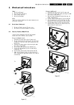
Page 19: ...g the cable from red connector 0201 4 Turn the panel 90 degrees counter clockwise 3 5 Flip the panel 90 degrees 4 with the components towards the CRT 6 Turn the panel with the rear I O towards the CRT 5 7 Slide the metal heatsink near the mains transformer 5520 underneath the right chassis bracket so the panel is secured 6 Figure 4 1 Main panel with bracket 1 Disconnect the strain relief of the AC...

Page 20: ...mps 2 and lift the board out of the bracket Figure 4 3 4 4 Rear Cover Mounting Before you mount the rear cover perform the following checks 1 Check whether the AC power cord is mounted correctly in its guiding brackets 2 Replace the strain relief of the AC power cord into the cabinet 3 Check whether all cables are replaced in their original position CL 06532012_004 eps 030200 ...

Page 21: ... as given in this manual To override SW protections To start the blinking LED procedure Specifications Tuning frequency 475 25 MHz for PAL SECAM AP PAL 61 25 MHz channel 3 for NTSC sets AP NTSC Colour system PAL BG for AP PAL NTSC for AP NTSC All picture settings at 50 brightness colour contrast hue Bass treble and balance at 50 volume at 25 All service unfriendly modes if present are disabled lik...

Page 22: ... Figure 5 4 1 LLLL This is the operation hours counter It counts the normal operation hours not the standby hours 2 AAABCD X Y This is the software identification of the main micro controller A the project name L01 B the region E Europe A Asia Pacific U NAFTA L LATAM C the software diversity C NTSC D DVD N no TXT T TXT D the language cluster number X the main software version number Y the sub soft...

Page 23: ... Indicates if the V chip feature is enabled 8 Value indicates parameter levels at CSM entry CO CONTRAST CL COLOR BR BRIGHTNESS HU HUE SH SHARPNESS 9 Value indicates parameter levels at CSM entry VL VOLUME LEVEL BL BALANCE LEVEL AVL AUTO VOLUME LEVEL LIMITER DV DELTA VOLUME 10 Value indicates parameter levels at CSM entry only for stereo sets TR TREBLE BS BASS How to exit Use one of the following m...

Page 24: ...or located on the Main panel see also figure 8 1 suffix D The ComPair faultfinding program is able to determine the problem of the defective television ComPair can gather diagnostic information in two ways Automatic by communication with the television ComPair can automatically read out the contents of the entire error buffer Diagnosis is done on I2C level ComPair can access the I2 C bus of the te...

Page 25: ... the error buffer is not reset When you transmit the command DIAGNOSE 99 OK with ComPair If the content of the error buffer has not changed for 50 hours it resets automatically 5 5 3 Error Codes In case of non intermittent faults clear the error buffer before you begin the repair These to ensure that old error codes are no longer present If possible check the entire contents of the error buffer In...

Page 26: ...tage at pins 1 3 4 5 and 6 are about 180 V and pin 8 is 0 V The reason why the voltage on these pins is so high is because the output driver pin 6 has an open load That is why MOSFET TS7521 is not able to switch Reason feedback resistor 3523 is defective Caution be careful measuring on the gate of TS7521 circuitry is very high ohmic and can easily be damaged first connect measuring equipment to gr...

Page 27: ...RT without any OSD info 7 Set the channel of the oscilloscope to 50 V div and the time base to 0 2 ms external triggering on the vertical pulse 8 Ground the scope at the CRT panel and connect a 10 1 probe to one of the cathodes of the picture tube socket see diagram B 9 Measure the cut off pulse during first full line after the frame blanking see Fig 8 2 You will see two pulses one being the cut o...

Page 28: ...64 242 144 44 21PT2301 67R 160 215 193 168 254 16 44 21PT2301 71R 160 215 193 162 254 144 36 21PT2301 74R 160 215 193 168 254 144 44 21PT2301 97R 160 215 193 162 254 144 36 21PT2302 56A 160 247 193 168 254 144 44 21PT2302 57R 160 247 193 168 254 144 44 21PT2302 65R 160 247 193 168 254 144 44 21PT2302 68R 160 247 193 168 254 144 44 21PT2302 69R 160 247 193 168 254 144 44 21PT2302 73R 160 247 193 16...

Page 29: ...DE is set to 1 After installation is finished this option bit will be automatically set to 0 Default setting 0 OP12 UK_PNP 0 UK s default Plug and Play setting is not available or not applicable 1 UK s default Plug and Play setting is available When UK_PNP and VIRGIN_MODE are set to 1 at the initial set up LANGUAGE ENGLISH COUNTRY GREAT BRITAIN and after exiting from menu VIRGIN_MODE will be set a...

Page 30: ...40 STEREO_NON_DBX 0 For AP_NTSC chip TDA 9853 is not present 1 For AP_NTSC chip TDA 9853 is present Default setting 0 OP41 STEREO_DBX 0 For AP_NTSC chip MSP 3445 is not present 1 For AP_NTSC chip MSP 3445 is present Default setting 0 OP42 STEREO_PB 0 For AP_PAL chip MSP3465 is not present 1 For AP_PAL chip MSP3465 is present Default setting 0 OP43 STEREO_NICAM_2CS 0 For EU and AP_PAL chip MSP 3415...

Page 31: ...e two option bits are allocated for LATAM system selection 00 NTSC M 01 NTSC M PAL M 10 NTSC M PAL M PAL N 11 NTSC M PAL M PAL N PAL BG Default setting 00 OP70 71 and 72 SOUND_SYSTEM_AP_1 SOUND_SYSTEM_AP_2 SOUND_SYSTEM_AP_3 These three option bits are allocated for AP_PAL sound system selection 000 BG 001 BG DK 010 I DK 011 BG I DK 100 BG I DK M Default setting 00 OP73 COLOR_SYSTEM_AP This option ...

Page 32: ... and input a crosshatch test pattern Set the generator amplitude to at least 1 mV and set frequency to 61 25 MHz channel 3 1 Set Smart Picture to NATURAL or MOVIES 2 Activate the SAM menu see chapter 5 3 Go to the GEOMETRY sub menu 4 Choose HORIZONTAL or VERTICAL alignment Now you can perform the following alignments Horizontal Horizontal Parallelogram HP Align straight vertical lines in the top a...

Page 33: ...Switch the blanking of the lower half of the screen ON or OFF to be used in combination with the vertical slope alignment H60 Align straight horizontal lines if NTSC input 60 Hz is used i s o PAL 50 Hz V60 Align straight vertical lines if NTSC input 60 Hz is used i s o PAL 50 Hz Figure 8 10 In the table below you will find the GEOMETRY default values for the different sets Figure 8 11 8 3 5 Audio ...

Page 34: ...ignal processor IC and the audio output IC via the I2 C bus The memory IC retains the settings for favourite stations customer preferred settings and service factory data The on screen graphics and closed caption decoding are done within the microprocessor and then sent to the signal processor IC to be added to the main signal The chassis uses a Switching Mode Power Supply SMPS for the main voltag...

Page 35: ...e the audio signal The signal then goes to pin 40 of IC7200 The internal input switch selects the following input signals Pin 40 terrestrial CVBS input Pin 42 external AV1 CVBS input Pin 44 external Side I O CVBS or AV2 Luminance Y input Pin 45 external AV2 Chrominance C input Figure 9 5 Once the signal source is selected a chroma filter calibration is performed The received colour burst sub carri...

Page 36: ... limiting A beam current limiting circuit inside the UOC handles the contrast and brightness control for the RGB signals This prevents the CRT from being overdriven which could otherwise cause serious damage in the line output stage The reference used for this purpose is the DC voltage on pin 54 BLCIN of the TV processor Contrast and brightness reduction of the RGB output signals is therefore prop...

Page 37: ...ntial inputs As the driver device IC7200 delivers output currents R3474 and R3475 convert them to voltage The differential input voltage is compared with the voltage across measuring resistor R3471 that provides internal feedback information The voltage across this measuring resistor is proportional to the output current which is available at pins 4 and 7 where they drive the vertical deflection c...

Page 38: ... a hard switching fixed frequency Flyback converter The efficiency can be improved up to 90 which results in lower power consumption Moreover the supply runs cooler and safety is enhanced The power supply starts operating when a DC voltage goes from the rectifier bridge via T5520 R3532 to pin 8 The operating voltage for the driver circuit is also taken from the hot side of this transformer The swi...

Page 39: ...nt IL will decrease In other words the transformer will be demagnetised When the inductive current has become zero the next interval begins Interval 4 t3 t t00 resonance time In the fourth interval the energy stored in the drain capacitor CD will start to resonate with the inductance LP The voltage and current waveforms are sinusoidal waveforms The drain voltage will drop from VIN n VOUT to VIN n ...

Page 40: ... of 75 mV This fixed VCO level is called VVCO start The frequency will be reduced in relation to the VCO voltage between 75 mV and 50 mV at levels larger than 75 mV Ctrl voltage 1 425V the oscillator will run on maximum frequency foscH 175 kHz typically At 50 mV VVCO max the frequency is reduced to the minimum level of 6 kHz Valley switching is still active in this mode Minimum Frequency mode MinF...

Page 41: ...on the load t3 Charge of VCC when gate drive is inactive The third interval starts when the UVLO is reached The internal current source charges the VCC capacitor also the soft start capacitor is recharged Once the VCC capacitor is charged to the start up voltage the driver is activated and a new burst cycle is started Figure 9 15 9 6 3 Protection Events The SMPS IC7520 has the following protection...

Page 42: ...video processing sound IF vision IF synchronisation etc 9 7 3 User Interface There are two control signals called KEYBOARD_protn and IR Users can interact either through the Remote Control transmitter or by activation of the appropriate keyboard buttons The L01 uses a remote control with RC5 protocol The incoming signal is connected to pin 67 of the UOC The Top Control keyboard connected to UOC pi...

Page 43: ...hanisms are built in over current and over voltage In case of over current due to defective parts in the line deflection output stage a high current will flow through resistors 3405 3406 If this current is large enough to create a voltage drop of 0 7 V across 3405 3406 transistor TS7606 in A7 diagram will conduct and pin 80 of the UOC will be pulled down Thereafter the UOC will shut down the power...

Page 44: ... is not transmitted off air NVM Non Volatile Memory IC containing TV related data e g alignments OB Option Byte OC Open Circuit OSD On Screen Display PAL Phase Alternating Line Colour system mainly used in West Europe colour carrier 4 433619 MHz and South America colour carrier PAL M 3 575612 MHz and PAL N 3 582056 MHz PCB Printed Circuit board PIP Picture In Picture PLL Phase Locked Loop Used for...

Page 45: ...375 90157 1K6V 13nF 2467 2222 347 90219 400V 15nF 2467 4822 121 40488 22nF 10 400V 2467 5322 121 44151 33nF 10 400V 2468 2222 347 90219 POL 347 400V 15nF 2468 5322 121 42532 18nF 10 400V 2471 5322 121 42386 100nF 5 63V 2472 4822 121 41854 150nF 5 63V 2473 5322 121 42386 100nF 5 63V 2474 4822 122 33127 2 2nF 10 63V 2475 4822 122 33127 2 2nF 10 63V 2476 5322 126 10223 4 7nF 10 63V 2480 5322 121 1047...

Page 46: ...2 11215 DSP301N A21F 3508 4822 116 83872 220W 5 0 5W 3510 4822 117 12765 4W7 20 3W1 3519 4822 116 83876 270W 5 0 5W 3520 4822 051 20122 1k2 5 0 1W 3521 4822 116 52186 22W 5 0 5W 3522 4822 051 20394 390k 5 0 1W 3523 4822 052 10479 47W 5 0 33W 3524 4822 117 11148 56k 1 0 1W 3525 4822 051 10102 1k 2 0 25W 3526 3198 012 11570 1W 0W15 3527 4822 117 11744 0W22 5 1W 3528 4822 051 20109 10W 5 0 1W 3529 48...

Page 47: ... 29RF 1018 3139 127 29321 CRT pnl 25RF 1018 3139 178 67421 CRT pnl 29FS 0141 4822 492 70788 FIX IC 0244 4822 265 30735 CON 5P 0245 2422 025 04854 CON V 6P F 0254 2422 500 80053 CON CRT 9P F DAF 0254 2422 500 80067 CON CRT V 9P F N NECK B 0278 4822 267 10735 CON B3B EH A 2330 4822 121 51473 470nF 20 63V 2340 4822 124 11565 10mF 20 250V 2341 4822 126 13599 3 3nF 10 500V 2342 5322 122 31647 1nF 10 63...

Page 48: ...Spare Parts List GB 88 L01 1A 10 ...

Page 49: ...DULATOR BTSC NDBX INPUT SWITCHING 3866 ERR 4 1861 514K5 A10 A9 A8 A7 A11 A6 3833 3834 2847 A13 A10 BTSC DBX STEREO SAP DECODER A9 7831 MSP34X5G QSS AM DEM OUT FMR 47 A5 MONO AM MONO SOUND 7834 7835 6692 TSOP1836 3V3 MAIN OUT L 44 A10 SC1 L IN 41 A10 SC1 R IN 42 A7 SDA 8 A7 SCL 7 25 4 SC2 CTRL A13 30 R OUT L OUT A5 A5 A7 A5 MONO AM MONO SOUND 31 MAIN OUT R 24 51 52 DEMODULATOR BTSC AM FM 3832 ERR 1...

Page 50: ... div A8 1V div DC 500us div A8a 1V div DC 500us div A9 500mV div DC 500us div A10 500mV div DC 500us div A11 1V div DC 200us div A11a 500mV div DC 2us div C1 1V div DC 500us div C2 1V div DC 500us div F1 500mV div DC 5ms div F2 500mV div DC 5ms div F3 10V div DC 5ms div F4 5V div DC 5ms div I1 2V div DC 200us div I2 2V div DC 200us div I3 500mV div DC 10us div I4 20mV div DC 10us div L1 1V div DC ...

Page 51: ...SED 5V TO 2234 VLOT AUX VLOT AUX 5V TO 3619 8V TO 7101 C VLOT AUX 5V AUDIO AMPLIFIER A8 PIP P 8V TO 3948 3950 VLOT AUX 5V TO 9904 8VA MAIN AUX_FB 1 1 2 40 24 25 3 5V 3460 9420 7471 FRAME OUTPUT 7330 RGB DRIVER 6 3 5001 5472 SYNCHRONISATION A6 7200 D SYNC PROC 5241 5890 7891 5893 9810 8V 13V VLOT AUX 50V 8V 8V 8V 8V 8V 8VA TO 3248 7200 A VIDEO IF 9 5832 BTSC DECODER A9 BTSC NDBX DECODER A11 VLOT AU...

Page 52: ...562 C9 3563 C10 2K2 3532 3564 B10 3565 A9 3566 G8 3567 C9 3568 C10 4K7 3531 3569 F8 3509 470R 3580 A9 5500 B4 5501 B3 5502 A5 5520 C7 5521 D7 5560 D8 5561 D10 5562 C8 5564 D9 6500 B6 6520 E2 6522 D2 6523 D5 6524 D7 6525 E7 6540 F9 6541 E9 6560 D9 6561 B9 6562 C9 6563 C9 6565 A11 6566 F10 6567 D10 6569 G9 6570 G8 6580 A9 6581 A8 7515 E7 7520 D3 7521 C6 7522 C5 7540 F9 7541 F8 7542 F8 7560 A10 7561 ...

Page 53: ...A9 2484 D6 2485 B10 2486 D9 3 4 5 6 7 8 9 10 11 A B C D E F G A B C D E F G 0220 A2 0221 B6 1400 B4 2400 F4 2401 F4 2402 F4 2404 G5 2405 D3 2415 D3 4R7 3411 1 2 3 4 5 6 7 8 9 10 11 1 2 4R7 3494 330R 3468 5450 BZX79 C6V8 6462 330n 2491 470n 2484 3457 1K 1K 3456 BZX384 C10 6453 BC857B 7450 5452 100MHZ 2490 2u2 6R8 3455 3409 2453 3450 100R 1M 3443 2443 47n 2415 2461 2405 4R7 3488 2456 6468 BAS216 349...

Page 54: ... 100K 2n7 2476 6470 BAV99 3495 22K 3498 12K 47n 2472 3480 4R7 3473 3477 150R 3472 2K2 3474 3471 100n 2473 3475 2K2 100n 2471 3479 2K7 6476 3470 2n2 2474 7 VOA 4 VOB 8 VOG 3 VP 2475 2n2 TDA8359J 7471 5 GND 6 VFLB 1 VI 2 VI 9 VM Vdrive Vdrive VlotAux 13V VlotAux 50V Vguard VlotAux 5V CL 16532053_053 eps 100701 0222 C6 2471 B3 2472 C4 2473 B5 2474 C1 2475 D1 2476 C5 3470 B4 3471 D5 3472 D5 3473 D5 34...

Page 55: ...008 D5 3009 D6 3010 D3 3011 D4 4001 D5 4002 E7 4003 E6 4004 E7 4005 D6 4006 D5 4011 F7 4012 F7 5001 A6 5002 C5 5003 F8 6001 A5 6002 B6 6003 C6 6004 D5 6005 D6 7001 E5 7002 E6 9001 D6 10n 2003 2005 10u 1K 3011 100R 3010 0283 0285 6002 BAS216 6001 BZX79 C33 100R 3000 3001 100R 22K 3004 4012 4001 4004 4011 9001 4003 4006 4005 PDTC124ET 7002 2010 1n 7001 PDTC124ET 2u7 5003 820n 5002 2002 3009 2K2 2001...

Page 56: ...3232 C11 3233 F7 3234 E10 3235 E2 3236 F7 3237 F8 3238 G7 3235 100R 3239 G8 3240 F6 3637 C1 3638 D1 4203 B8 4204 C8 4205 E2 4206 F2 4207 E2 4209 D9 4210 B8 4211 B8 4212 B2 4213 A2 4214 D10 7209 BFS20 4216 F9 5201 D7 0248 5202 A9 5203 F8 5204 F2 5205 F2 5206 F3 6201 F4 6202 F5 6203 F8 6204 F9 6206 G4 7200 A B9 7200 C C3 7201 D8 7202 E8 7203 E7 7204 F5 820p 2233 7205 A4 100n 2204 7206 B7 7208 B6 720...

Page 57: ...00n 5 1 2 3 10u 5242 2247 B5 2248 B5 2249 C3 2250 C1 2252 C5 2253 C5 2254 B2 3241 D2 3242 C1 3244 C5 3245 E3 3246 D3 3247 E5 3248 D5 3249 C5 3250 D5 3251 B5 3254 B5 3256 B5 3257 B3 3258 B2 3259 B1 5241 A5 5242 B5 7200 D C2 3254 1M 2254 100p 3259 470K 10M 3258 330K 3257 2253 1n 1K 3256 1n 2252 2u2 2250 2249 22n 2248 22n 1m 2247 2246 4u7 5241 10u 27K 3242 100R 3250 3248 220K 3247 27K 10K 3246 1n 224...

Page 58: ...622 D8 3623 D3 3624 B8 3625 B8 3626 C8 3627 C9 3628 D8 3629 C9 3630 D8 3632 D9 3633 D9 3634 C8 3635 B2 B C D E F G A B C D E F G 0217 F3 0240 A3 0250 A2 0261 D2 0273 A5 0274 A9 0279 C3 1660 E7 2601 A7 2602 D9 2604 E2 2606 E8 2607 D8 2608 A6 2609 E8 2611 B6 2612 C8 2613 B8 2615 A7 1 2 3 4 5 6 7 8 9 10 1 2 3 4 5 6 7 8 9 10 A 1u 2619 2618 10n 9647 47n 2616 0274 0279 0273 9631 4618 9641 1 2 3 4 5 6 46...

Page 59: ...04 C3 4905 F2 4921 B4 6901 B5 7901 B6 7902 D6 7943 F4 9901 C8 9902 C8 9903 A3 9904 B3 CH1 6 CH1 IN 12 CH2 10 CH2 8 CH2 IN 3 GNDCH1 11 GNDCH2 7 GNDINP 5 STB 1 VCC 9 VOL AN7522N 7901 2 CH1 4 4903 100p 2949 AudioSupplyGnd_FB 100p 2947 2948 100p 4905 100p 2950 2911 10n 6K8 3172 0281 1 2 3 4 3 4 0280 1 2 3 4 0275 0271 1 2 STB 5 VCC 1 VOL 9 AudioSupplyGnd_FB 7902 AN7523N CH1 2 CH1 4 CH1 IN 6 GNDCH1 3 GN...

Page 60: ... 6 7 8 9 10 11 7835 BC847B 2833 D4 2834 B3 2835 B4 2836 B4 1n 2859 2837 B4 2838 B10 2839 B10 2840 B6 2841 C5 2842 A7 2843 A7 2844 C3 2845 C3 2846 G2 2847 D3 2848 D3 2849 C10 2850 D10 2851 E10 2852 E9 2853 F10 2854 F9 4834 2855 E2 3841 33K 2856 E3 2857 F2 2858 F4 2859 G2 2860 F3 2894 A7 2895 A7 2896 F3 2897 C3 2898 B6 3831 B3 1K 3836 3832 A10 3833 B10 3834 D2 3835 D3 3836 E9 3837 E8 3838 F9 3839 E8...

Page 61: ...V6 5V8 3V8 1V6 5V 1V6 5V8 0V 0V 5V 0V 1V8 6V 2V5 1V8 6V 2V3 3806 100K 3803 100K 2801 B4 2802 E4 2803 C2 2804 C5 2805 D5 1 2 3 4 5 6 7 1 2 3 4 5 6 7 A B C D E F G A B C D E F G 1K 3802 3801 A2 3802 A2 3803 C4 4802 3804 C4 3805 C5 3806 D4 3807 D4 3808 D5 3809 G2 4801 C6 4802 C6 4803 D6 4804 D6 4805 E2 4806 F1 4807 G3 4808 G3 4809 B2 7801 B3 7802 A E3 7802 B F3 7802 C G3 7803 C5 7804 D5 9801 E2 3809 ...

Page 62: ...3 G2 2984 G3 3181 B3 3182 A3 3183 B3 3184 B3 3185 C3 3186 C3 3681 A8 3682 A9 3683 A7 3684 A8 3685 A7 3686 C8 3691 C9 3692 E8 3693 D10 3694 D9 3695 D7 3981 F3 3982 G3 4691 E8 4692 D7 4693 E7 4694 H1 4695 D9 6181 B4 6681 B8 6691 D8 6692 D9 9181 B5 9982 F2 6181 3693 220R 560R 3685 4691 1603 75R 3181 AudioSupplyGnd_FB AudioSupplyGnd_FB 2696 100p 2694 100p 100p 2695 100p 2693 0286 4695 2186 100p 0278 0...

Page 63: ... C4 3115 D3 3116 D4 3121 F3 3122 F3 3123 F3 3124 F4 0242 1 2 3 4 5 6 7 3125 G3 22p 1K 3102 3126 G4 3131 B8 3132 B7 3133 B8 3134 B7 3135 C8 3136 C7 1K 3141 3137 D8 3138 D7 3141 F8 3151 C5 3152 C5 3153 D5 3154 D1 3156 D1 3157 E1 3158 D2 3159 E1 4101 B3 4102 B3 4104 B3 4121 E6 4131 C9 7101 A6 7102 D2 7103 E1 9101 D4 9102 C4 3158 10K 3159 820R 2143 100n 3156 10K 0226 1 2142 2u2 5K6 3154 BC857B 7102 BC...

Page 64: ...PERATURE PROTECTION TDA8941P TILT ROTATION A8 74 TO ROTATION COIL 0268 B8 2171 B4 2172 B5 3171 B4 3173 B4 3174 B5 7000 B6 L13 L14 1 2 3 4 5 6 7 8 1 2 3 4 5 6 7 8 A B C D GND IN IN MODE OUT OUT SVR Vcc 0268 1 2 3 68K 3173 7000 2172 220p 3171 120K 2171 100p Tilt VlotAux 13V VlotAux 13V 3174 68K CL 16532053_071 eps 100701 A15 ...

Page 65: ... B4 3173 C4 3174 C5 3175 C5 3176 C6 3177 D4 3178 D5 3179 D6 7171 B4 7172 C6 7173 D5 7174 D4 V20 V21 1 2 3 4 5 6 7 8 1 2 3 4 5 6 7 8 0284 1 2 3 4 3179 2K2 2171 1n8 3178 3K9 3176 8K2 10K 3173 3175 8K2 3174 8K2 3177 8K2 7173 BC847B 7172 BC857B 7174 BC857B 10K 7171 BC857B 3170 68K 3171 HD VlotAux 5V VD VlotAux 5V SANDCASTLE CL 16532053_064 eps 100701 ...

Page 66: ...44 L01 1A 7 Schematics and PWB s Layout Large Signal Panel Top View CL 16532053_005 eps 050601 ...

Page 67: ...arge Signal Panel Mapping Top View Layout Large Signal Panel Overview Bottom View CL 16532053_006 eps 100701 Part 1 CL 16532053_06a eps Part 3 CL 16532053_06c eps Part 4 CL 16532053_06d eps Part 2 CL 16532053_06b eps CL 16532053_05m eps 100701 ...

Page 68: ...46 L01 1A 7 Schematics and PWB s Layout Large Signal Panel Part 1 Bottom View Part 1 CL 16532044_86a eps 310501 ...

Page 69: ...Schematics and PWB s 47 L01 1A 7 Layout Large Signal Panel Part 2 Bottom View Part 2 CL 16532053_06b eps 310501 ...

Page 70: ...48 L01 1A 7 Schematics and PWB s Layout Large Signal Panel Part 3 Bottom View CL 16532053_06c eps 040601 Part 3 ...

Page 71: ...Schematics and PWB s 49 L01 1A 7 Layout Large Signal Panel Part 4 Bottom View Part 4 CL 16530153_06d eps 050601 ...

Page 72: ...4 3334 B5 3335 C4 3336 B5 3340 E2 3341 E4 3342 E4 3343 E5 3344 E6 3345 D6 3346 E6 3347 B1 3348 B2 3349 B2 3350 B1 3351 C2 3352 C2 0245 3353 C1 3354 D2 3355 D2 5342 C5 5343 B2 5344 B2 5345 C2 6331 B4 6332 D3 6333 B4 6335 B4 7330 B2 9341 A2 9342 B2 9343 C2 6 7 8 9 1 0165 200VA 3346 22R 10u 2340 9342 2344 100n 9341 6332 BAS216 1K 3354 100R 3353 SDL 5345 3355 2K2 3350 100R 3352 2K2 3351 1K 5344 SDL 10...

Page 73: ... D6 3377 D7 3378 D8 3379 D3 3382 E6 3383 E5 3384 E8 3385 E9 3386 D3 3387 D4 3388 E7 3389 E7 3390 C7 3391 D7 5360 B3 5361 D9 5362 D9 6360 C5 7360 C6 7362 C8 7363 D6 7365 D9 7366 E7 7367 D4 9361 B3 9363 D9 9364 D9 9365 C5 9366 D7 3376 150p 2375 33R 3390 3391 33R 1n 2373 1n 2374 3388 220R 3389 220R 9366 9365 2372 5p6 3387 470K 7367 BC557B 22p 2371 3386 2K2 2K2 3379 2367 150p 680R 3361 9361 9363 9364 ...

Page 74: ... 3389 A2 5342 A2 5343 A1 5344 A1 5345 A1 5360 A2 5361 A2 5362 A2 6331 A1 6333 A1 6335 A1 6360 A1 7330 A1 7360 A1 7362 A2 7363 A1 7365 A2 7366 A2 7367 A1 9311 A1 9341 A1 9342 A1 9343 A1 9361 A2 9363 A2 9364 A2 9365 A1 9366 A2 CL 16532053_011 eps 110501 Layout CRT Panel Bottom View CL 16532053_011 eps 110501 2342 A1 2344 A1 2364 A1 2367 A1 2368 A2 2369 A1 2371 A1 2372 A1 2373 A1 2374 A1 2375 A2 3347...

Page 75: ... 2176 F3 2177 F3 2178 E3 2179 E3 1 2 3 4 5 6 1 2 3 4 5 6 A B C D E F A B C D E SG07 3150 D4 3151 D4 3152 C4 3153 B4 3155 B4 3156 E3 3157 F3 6161 B4 9152 C3 9153 B4 SG02 B3 SG03 D3 SG04 C3 SG06 F4 SG07 E4 SG06 0277 A 0277 B 3157 1 2 3 4 5 3156 0254 100u 2177 2176 2179 100u 6 7 8 9 2178 4 0232 1 2 3 4 5 0255 1 2 3 2173 330p 2172 9153 9152 0251 1 2 3 4 5 6 7 8 9 3155 75R 0250 C 1 2 3 0250 A 0250 B 4 ...

Page 76: ...E A B C SG06 0252 B2 0253 A5 0254 D2 0255 D5 0261 C5 2171 C4 2172 B4 2173 B3 2174 C3 2176 E3 2177 E2 2178 E3 2179 D2 3150 C3 3151 C3 3152 B3 3153 B3 3155 A3 3156 D3 3157 E3 6161 A3 9153 B3 9155 B4 SG02 A3 SG03 C3 SG04 B3 SG06 E3 SG07 E3 4 1 2 3 4 0255 1 2 3 0251 1 2 3 0252 0253 1 2 3 3157 9155 3156 0254 1 2 3 4 5 2174 2177 100u 2176 100u 2179 3 4 5 6 7 8 9 2178 2172 330p 0232 1 2 2173 1 2 3 4 5 6 ...

Page 77: ...1K2 3858 2857 3857 0216 1 2 3 4872 4870 4871 4800 2896 4801 9801 3825 5893 2817 10p 150R 12MHZ 1800 HC 49 U 3826 150R 1801 HC 49 U 12MHZ 2818 10p 2859 470n 3856 BC847B 7816 3966 3835 3864 3871 9810 3870 3872 10n 2837 10u 2804 3860 BAT85 6801 15K VIN_ADC 22 VIN_Sync 23 VOUT 35 VRB 20 VRT 21 28 Xtal_NTSC Xtal_PALM 29 30 Xtal_PALN YOUT 39 3854 FILTER 26 FSC 10 HD 32 MCK 17 14 RESET SCK 8 SCLK 4 SDATA...

Page 78: ...56 L01 1A 7 Schematics and PWB s Layout PIP Panel Top View CL 16532010_010 eps 210301 ...

Page 79: ...Schematics and PWB s 57 L01 1A 7 Layout PIP Panel Bottom View CL 16532010_011 eps 210301 ...

Page 80: ...215 A1 1091 B2 1092 B3 1093 B3 1094 C3 2010 B1 3091 A1 3092 A2 3093 A2 3094 A3 3095 A3 3096 C3 6091 B3 BAT85 6091 2010 10n 3095 3K3 3096 1K5 3094 270R 3092 390R 560R 3093 3 3091 560R 0215 1 2 1094 1092 1093 1091 CL 16532053_069 eps 100701 Top Control Panel RF Top View 1091 A1 1092 B1 1093 A2 1094 A1 6091 A1 CL 16532020_059 eps 030401 ...

Page 81: ... B C 0215 A1 1091 B2 1092 B3 BAT85 6091 1093 B3 1094 C3 2010 B1 3091 A1 3092 A2 3093 A2 3094 A3 3095 A3 3096 C3 6091 B3 3096 1K5 3094 270R 3095 3K3 3092 390R 560R 3093 3091 560R 0215 1 2 3 1094 1092 1093 1091 CL 16532020_054 eps 200301 Top Control Panel FSQ Top View 0215 A2 1091 A2 1092 A1 1093 A2 1094 A1 6091 A2 CL 16532020_100 eps 050601 ...

Page 82: ...M 9503 A1 X X X X X X X X X X X X X X X WR CU ETP SNPB5 PL 0 58MM 9506 A1 WR CU ETP SNPB5 PL 0 58MM 9507 A1 Diagram A1 Diagram A2 12NC Description Item Schematic FB 21PT2252 69R AP L01L FB 21PT2301 67R AP L01L FB 21PT2301 71R AP L01L FB 21PT2302 56A AP L01L FB 21PT2302 69R AP L01L FB 21PT2251 67R AP L01L FB 21PT2251 71R AP L01L FB 21PT2252 56A AP L01L FB 21HT2212 67R AP ITV L01L FB 21HT2211 68Z AP...

Page 83: ...252 97R AP L01L FB 21PT2301 97R AP L01L FB 29PT2565 93R CH L01L FB 21PT2565 93R CH L01L FB 25PT2565 93R CH L01L FB 29PT2566 93R CH L01L FB 21PT2452 94R IN L01L FB 25PT2435 94R IN L01L FB 21PT2251 97R AP L01L FB 21PT2251 71R AP L01L FB 25PT2511 93R CH L01L FB 25PT2521 93R CH L01L FB 29PT2525 93R CH L01L FB 29PT2535 93R CH L01L FB 25HT2217 93Y AP ITV L01L FB 21HT2212 93R AP ITV L01L FB 29HT2217 93Y ...

Page 84: ... L01L FB 21PT2251 67R AP L01L FB 21PT2251 74R AP L01L FB 21PT2301 74R AP L01L FB 21PT2555 93R CH L01L FB 21PT2301 71R AP L01L FB 21PT2251 71R AP L01L FB 21PT2251 97R AP L01L FB 21PT2301 97R AP L01L FB 21HT2212 93R AP ITV L01L FB 21HT2212 69R AP ITV L01L FB 21HT2212 67R AP ITV L01L FB 21HT2211 68Z AP ITV L01L FB 21PT2452 94R IN L01L FB 25PT2252 69R AP L01L FB 25PT2252 56A AP L01L FB 25PT2252 79R AP...

Page 85: ...55 93R CH L01L FB 21HT2212 93R AP ITV L01L FB 21HT2212 69R AP ITV L01L FB 21HT2212 67R AP ITV L01L FB 25PT2511 93R CH L01L FB 25HT2012 93R AP ITV L01L FB 25HT2012 79R AP ITV L01L FB 25HT2212 69R AP L01L FB 25PT2152 69R AP L01L FB 25PT2252 69R AP L01L FB 25PT2152 65R AP L01L FB 25PT2252 57R AP L01L FB 25PT2152 68R AP L01L FB 25PT2252 68R AP L01L FB 25PT2455 94R IN L01L FB 25PT2152 67R AP L01L FB 25...

Page 86: ...A13 X X X X X X X X X X X X X X X X X X X X X X X X X X X X X X X X X X X X X X X X X X X X X X X X X X X X X X X X X X X X X X X X X X X X X X X 47K 3134 A13 X X X X X X X X X X X X X X X X X X X X X X X X X X X X X X X X X X X X X X X X X X X X X X X X X X X X X X X X X X X X X X X X X X X X X X X 75R 3135 A13 X X X X X X X X X X X X X X X X X X X X X X X X X X X X X X X X XX X X X X X X X X X X...

Page 87: ...01L FB 21PT2452 94R IN L01L FB 21PT2465 94R IN L01L FB 25PT2435 94R IN L01L FB 21PT2301 67R AP L01L FB 21PT2301 71R AP L01L FB 21PT2302 56A AP L01L FB 21PT2302 69R AP L01L FB 25PT2152 56A AP L01L FB 25PT2152 67R AP L01L FB 25PT2152 71R AP L01L FB 29PT2152 56A AP L01L FB 29PT2152 67R AP L01L FB 29PT2152 71R AP L01L FB 29PT2152 79R AP L01L FB 34PT2152 79R AP L01L FB 21PT2251 67R AP L01L FB 21PT2251 ...

Page 88: ...66 L01 1A 7 Schematics and PWB s Personal Notes Personal Notes ...

Reviews: