


1
2
3
4
5
6
A
B
C
D
6
5
4
3
2
1
D
C
B
A
Title
Number
Revision
Size
B
Date:
10-Oct-2002
Sheet of
File:
D:\wzw\Myproj\isp1301\eva_kit\eva board\pcb\02226-1.ddb
Drawn By:
1
14
2
15
3
16
4
17
5
18
6
19
7
20
8
21
9
22
10
23
11
24
12
25
13
J10
DB25(MALE)
11
10
U2E
74HCT05
5
6
U2C
74HCT05
3
4
U2B
74HCT05
9
8
U2D
74HCT05
1
2
3
4
5
6
7
8
9
10
11
12
13
14
15
16
17
18
19
20
21
22
23
24
25
26
27
28
29
30
31
32
33
34
35
36
37
38
39
40
J13
HEADER20X2
C29
18pF
C30 18pF
C31 18pF
+
C18
10uF
uP5V
CLK
1
SDA
2
SCL
3
IACK_N
4
INT_N
5
A0
6
D0
7
D1
8
D2
9
GND
10
D3
11
D4
12
D5
13
D6
14
D7
15
RD_N
16
CS_N
17
WR_N
18
RESET_N
19
VDD
20
U4
PCF8584
D0
D1
D2
D3
D4
D5
D6
D7
D8
D9
D10
D11
D12
D13
D14
D15
A0
WR_N
RD_N
CS_N
D0
D1
D2
D3
D4
D5
D6
D7
D[0..15]
14
7
1
2
U2A
74HCT05
INT1
INT2
uP5V
uP33V
+
C20
10uF
uP33V
R17 10K
R18
10K
R19
10K
+5V
A0
3
4
U3B
74HCT04
1
2
7
14
U3A
74HCT04
SDA_8584
SCL_8584
+5V
RESET_N
CLK
INT_N
S3
C3#
D7
S7#
SDAIN#
SDAOUT#
SCLIN
SCLOUT#
1
2
3
4
J11
I2C CONNECTOR
SCL5V
SDA5V
+5V
+5V
+3.3V
+
C25
10uF
+
C27
10uF
1
2
JP2
JUMPER
H_VBUS
uP5V
Ext5V
1
2
JP5
JUMPER
+3.3V
+3.3V
VBAT
VIO
+5V
VCC
4
CLOCK
3
NC
1
GND
2
Y1
12MHz OSC_HALF
+5V
C24
0.1uF
C19
0.1uF
C28
0.1uF
C26
0.1uF
C21
0.1uF
C22
0.1uF
C23
0.1uF
+5V
LED2
5.0V
R24
4.7K
1
2
3
J12
POWER JACK
Ext5V
Q2
ZVN4206
Q3
ZVN4206
R22
3.3K
R23
3.3K
VIO
R20
3.3K
R21
3.3K
+5V
SDA_PC
SCL_PC
SCL_8584
SDA_8584
1
2
3
JP3
HEADER 3
1
2
3
JP4
HEADER 3
SDA5V
SCL5V
SDA
SCL
AUD_EN
CHRG_EN
Vin
1
GND
2
Vout
3
Q4
LM1117DT33
1
2
3
4
5
6
JP6
HEADER 3X2
+5V
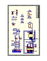
I2C MASTER / POWER
ISP1301 EVALUATION BOARD
V1.0
2/2
+5V
C51
0.1uF
C53
0.1uF
C52
0.1uF
+5V
+5V
+5V


