background image

UM10028_1 

ISP1301 USB OTG Transceiver  
Eval Kit User’s Guide


February 2003 


We welcome your feedback. Send it to 

[email protected]

Philips Semiconductors - Asia Product Innovation Centre 
Visit 

www.semiconductors.philips.com/buses/usb

 or 

www.flexiusb.com


User’s Guide 

Rev. 1.0 


Revision History: 

Version Date Descriptions


Author 

1.0 

Feb 2003 

First release 

David Wang 


Summary of Contents for ISP1301

Page 1: ...me your feedback Send it to wired support philips com Philips Semiconductors Asia Product Innovation Centre Visit www semiconductors philips com buses usb or www flexiusb com User s Guide Rev 1 0 Revision History Version Date Descriptions Author 1 0 Feb 2003 First release David Wang ...
Page 2: ...SCLAIMS ALL WARRANTIES INCLUDING WITHOUT LIMITATION ANY IMPLIED WARRANTIES OF MERCHANT ABILITY FITNESS FOR A PARTICULAR PURPOSE AND NONINFRINGEMENT THE ENTIRE RISK ARISING OUT OF THE USE OR PERFORMANCE OF THE PRODUCT AND DOCUMENTATION REMAINS WITH THE RECIPIENT TO THE MAXIMUM EXTENT PERMITTED BY APPLICABLE LAW IN NO EVENT SHALL PHILIPS SEMICONDUCTORS OR ITS SUPPLIERS BE LIABLE FOR ANY CONSEQUENTIA...

Page 3: ...or ISP1301 9 5 3 2 Reset all registers 9 5 3 3 List all registers 10 5 3 4 Read Write register 10 5 3 5 Select Mode of Operation 11 5 3 6 Enable Disable charge pump 11 6 HARDWARE DESCRIPTION 12 6 1 BLOCK DIAGRAM 12 6 2 FUNCTIONAL DESCRIPTION 12 6 2 1 PCF8584 I2 C bus controller 12 6 2 2 PC parallel to I2 C converter 12 6 2 3 HC DC and OTG core logic interface connector 12 6 2 4 Power manager 13 6 ...

Page 4: ...terface J3 pin assignment 14 Table 9 1 BOM of the ISP1301 evaluation board 17 FIGURES Figure 1 1 ISP1301 evaluation board PCB layout 5 Figure 4 1 Location of major components 8 Figure 5 1 Test program main menu 9 Figure 5 2 List all registers screen display 10 Figure 5 3 Read Write register screen display 11 Figure 5 4 Select Mode of Operation screen display 11 Figure 6 1 Block diagram of the ISP1...

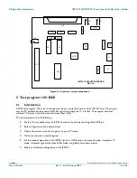
Page 5: ...to evaluate the functions of the ISP1301 chip The main components on the board are the ISP1301 in HVQFN24 package I2 C master USB mini AB connector analog audio interface and USB OTG controller interface The operation mode of the ISP1301 can be configured through the I2 C interface The OTG status and control registers in the ISP1301 can also be accessed through the I2 C interface To verify the fun...

Page 6: ...er default The power supply VBAT pin for the ISP1301 can be provided either from the onboard 3 3 V source or from the OTG Controller interface pin 2 of J3 Similarly the power supply for the VIO called VDD_LGC in the ISP1301 datasheet pin of the ISP1301 can be provided either from the onboard 3 3 V source or from the OTG Controller interface pin 2 of J8 Table 3 2 VBAT and VIO selection Jumper Descr...

Page 7: ...ame time If you have a system that consists of a USB host port and a separate device port then the host port can be connected to J4 and the device port can be connected to J1 using the standard USB cable In such a case the ISP1301 provides only OTG functions to the system the transceiver function of the ISP1301 is not used 3 4 Audio interface The ISP1301 evaluation board has an interface to suppor...

Page 8: ...chip The program uses the PC parallel port to access the ISP1301 registers through the I2 C interface The program simulates software I2 C master at the hardware abstraction layer HAL The test program can do the following Set the I2 C slave address for the ISP1301 based on the hardware setting of the ADR pin Reset all registers to their default values Display the current value of all registers on y...

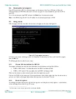
Page 9: ...any item 1 6 will perform the desired action If you wish to exit the program press the Esc key The following sections describe the menu items 5 3 1 Choose I2C slave address for ISP1301 The program will prompt you to enter your choice based on the hardware setting of the ADR pin If ADR is HIGH select 1 The slave address for the ISP1301 will become 0x5A If ADR is LOW select 0 The slave address for t...

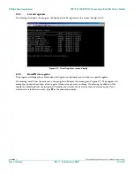
Page 10: ...s screen display 5 3 4 Read Write register The program will display the current value of all registers and prompt you to write to a specific register On selecting item 4 from the main menu the program will display the screen given in Figure 5 3 The program will prompt you to type the address of the register whose value you want to change On entering the address of the register and pressing Enter t...

Page 11: ...de four data encoding and decoding methods transparent I2 C mode transparent buffer mode USB suspend mode and global power down mode Note If the ISP1301 Engineering Sample 1 ES1 that is the chip whose version register reads 0x0100 or the chip package is marked AX is mounted on the evaluation board software cannot wake up the chip if set to the global power down mode Only a hardware reset can wake ...

Page 12: ...2 Functional description A brief description of each function module is given in the following sections 6 2 1 PCF8584 I 2 C bus controller This block provides functions of the I2 C bus to the 8 bit parallel bus converter It can connect to the Philips ISP1362 or ISP1161x ISA interface board or any other generic 8 bit microprocessor interface through a 40 wire IDE cable The PC or other microprocesso...

Page 13: ...de Required signals include D0 D7 A0 WR_N RD_N CS_N INT1 and INT2 Table 7 2 shows the pin assignment for J13 Note We use a 20 x 2 header to make it compatible with the Philips ISP1362 and ISP1161x ISA interface boards Table 7 2 8 bit microprocessor interface 20 x 2 header J13 pin assignment 1 Pin no Pin name Pin no Pin name Pin no Pin name Pin no Pin name 1 GND 11 n c 21 D7 31 D2 2 n c 12 3 3 V 22...

Page 14: ... interface J8 pin assignment Pin no Pin name Pin no Pin name 1 GND 9 GND 2 VIO 10 OE_TP_INT_N 3 GND 11 GND 4 INT_N 12 DAT_VP 5 GND 13 GND 6 SDA 14 SE0_VM 7 GND 15 GND 8 SCL 16 RCV Table 7 4 OTG Controller interface J3 pin assignment Pin no Pin name Pin no Pin name 1 GND 9 GND 2 VBAT 10 SPEED 3 GND 11 GND 4 n c 12 SUSPEND 5 GND 13 GND 6 ADR 14 VM 7 GND 15 GND 8 RESET_N 16 VP 8 Schematics of the eva...

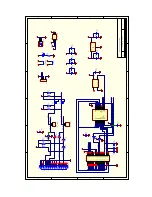
Page 15: ...5 10K C17 1uF VIO PAD 1 TP1 VBUS PAD 1 TP3 ID PAD 1 TP2 D PAD 1 TP4 D R11 100R R12 100R C7 220nF C8 220nF C9 220nF R16 100R A 1 B 2 C 3 J6 PHONEJACK STEREO SPK LINE IN J7 PHONEJACK MIC LINE OUT VBUS D D ID 1 4 7 8 5 6 2 3 Q1 PHP125 R4 0 R3 10K C5 0 1uF CHRG_EN 3 2 1 D1 STZ5 6N VBUS 1 D 2 D 3 GND 4 CHASSIS 5 J1 USB A RECEPTACLE VBUS 1 D 2 D 3 GND 4 CHASSIS 5 J4 USB B RECEPTACLE H_VBUS D D 5V C2 10u...

Page 16: ...A0 WR_N RD_N CS_N D0 D1 D2 D3 D4 D5 D6 D7 D 0 15 14 7 1 2 U2A 74HCT05 INT1 INT2 uP5V uP33V C20 10uF uP33V R17 10K R18 10K R19 10K 5V A0 3 4 U3B 74HCT04 1 2 7 14 U3A 74HCT04 SDA_8584 SCL_8584 5V RESET_N CLK INT_N S3 C3 D7 S7 SDAIN SDAOUT SCLIN SCLOUT 1 2 3 4 J11 I2C CONNECTOR SCL5V SDA5V 5V 5V 3 3V C25 10uF C27 10uF 1 2 JP2 JUMPER H_VBUS uP5V Ext5V 1 2 JP5 JUMPER 3 3V 3 3V VBAT VIO 5V VCC 4 CLOCK 3...

Page 17: ... 3 3K 4 R20 R21 R22 R23 0805 4 7K 2 R5 R24 0805 10K 10 R3 R6 R7 R8 R9 R10 R15 R17 R18 R19 0805 12MHz OSC_HALF 1 Y1 XTAL CTX ISP1301 1 U1 HVQFN24 74HCT05 1 U2 SOP14 74HCT04 1 U3 SOP14 PCF8584 I2C CONTROLLER 1 U4 DIP20 PHP125 P MOSFET POWER MOS 1 Q1 SO8 ZVN4206 N MOSFET 2 Q2 Q3 TO92 LM1117DT33 3 3V REGULATOR 1 Q4 TO252 STZ5 6N ESD DIODE 1 D1 SOT346 LED 2 LED1 LED2 Thru hole DB25 MALE 1 J10 Thru hole...

Page 18: ..._1 Koninklijke Philips Electronics N V 2003 All rights reserved User s Guide Rev 1 0 February 2003 18 of 18 10 References ISP1301 USB On The Go Transceiver datasheet Universal Serial Bus Specification Rev 2 0 On The Go Supplement to the USB 2 0 Specification Rev 1 0 ISP1301 Errata ...

Reviews: