background image

TABLE OF CONTENTS   


Page 

Service Manual 

. Mechanical and Dismantling Instructions…………........................3-1
. Software Upgrades 

..........................................

.............................

.

4-1

. Trouble Shooting Chart………………………………………………

.

5-1

. Wiring Diagram………………………………………..………..….….6-1 
. Electrical Diagrams and Print-layouts..….…………………....….…7-1     

. Set Mechanical Exploded view & Part list.…………………..….…10-1 

©Copyright 201

1

 Philips Consumer Electronics B.V. Eindhoven, The Netherlands 

All rights reserved. No part of this publication may be reproduced, stored in aretrieval system or 
transmitted, in any form or by any means, electronic, mechanical, photocopying, or otherwise 
without the prior permission of Philips. 

CLASS 1 

LASER PRODUCT

PHILIPS

GB

. DFU Instruction..............................................................................2-1

. Revision List.................................................................................11-1

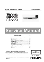
Home Theater Soundbar

. Technical Specifications…………....………………………..............1-

3

. Safety Instruction, Warning & Notes….……………………....….....1-

7

. Location of PCB

 Boards

 ,Version Variation and Repair Scenario Matrix....1-2

Published by 

Arya & Stephen

  - 1

23

4

 BU AVM   Printed in The Netherlands   Subject to modification

3141 785 38

360

Version 1.

1

Service

HTB5150D/12

. Votages and Waveforms for Connection Pins..….………………...8-1   
. Pin Description & Block Diagrams of ICs..….………………..........9-1   

. Pin Description & Block Diagrams of ICs..….………………..........9-1   

. Votages and Waveforms for Connection Pins..….………………...8-1   

Summary of Contents for HTB5150D/12

Page 1: ...al system or transmitted in any form or by any means electronic mechanical photocopying or otherwise without the prior permission of Philips CLASS 1 LASER PRODUCT PHILIPS GB DFU Instruction 2 1 Revision List 11 1 Home Theater Soundbar Technical Specifications 1 3 Safety Instruction Warning Notes 1 7 Location of PCB Boards Version Variation and Repair Scenario Matrix 1 2 Published by Arya Stephen 1...

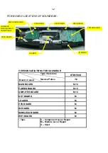
Page 2: ...BOARD M C KEY BOARD M LOADER M VFD BOARD M IN BOARD M WIRELESS BOARD M WIFI BOARD M Tips Board in used C Component Lever Repair M Module Lever Repair X Used 12 PCB BOARD LOCATION OF SOUNDBAR MAIN BOARD AMPLIFIER BOARD LOADER POWER BOARD IN BOARD 1 2 KEY BOARD VFD BOARD WIRELESS BOARD UNDER MAIN BOARD WIFI BOARD ...

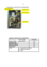
Page 3: ...150D Service Police POWER BOARD M AMPLIFER BOARD M WIRELESS BOARD M WIFI BOARD M Tips Board in used C Component Lever Repair M Module Lever Repair X Used 12 PCB BOARD LOCATION Of SUBWOOFER AMPLIFIER BOARD POWER BOARD 1 2 WIRELESS BOARD WIFI BOARD UNDER WIRELESS BOARD ...

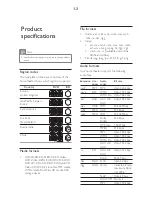
Page 4: ... RJJ Video avi divx mp4 m4v mov mkv m2ts DVI ZPY PSJ PSHJ ÁY JS J rmvb rm rv Available only in Asia 3DFLÀF DQG KLQD 3LFWXUH MSJ MSHJ MSH MLI MÀI MÀ JLI SQJ Audio formats Your home theater supports the following DXGLR ÀOHV Extension Con tainer Audio codec Bit rate mp3 MP3 MP3 Upto 320 kbps wma ASF WMA Upto 192 kbps WMA Pro Upto 768 kbps aac AAC AAC HE AAC Upto 192 kbps wav WAV PCM 27 648 Mbps m4a M...

Page 5: ...U Audio codec Video codec Bit rate Dolby Digital MPEG MP3 AAC HE AAC DD MPEG 1 MPEG 2 40 Mbps MPEG 4 ASP 38 4 Mbps H 264 AVC HiP 5 1 25 Mbps PRY ÀOHV LQ 029 FRQWDLQHU Audio codec Video codec Bit rate Dolby Digital MPEG MP3 AAC HE AAC MPEG 1 MPEG 2 40 Mbps MPEG 4 ASP 38 4 Mbps H 264 AVC HiP 5 1 25 Mbps PNY ÀOHV LQ 0 9 FRQWDLQHU Audio codec Video codec Bit rate PCM Dolby Digital DTS core MPEG MP3 WM...

Page 6: ...tio 65 dB CCIR A weighted Input sensitivity AUX 2V Music iLink 300 mV Video Signal system PAL NTSC HDMI output 480i 576i 480p 576p 720p 1080i 1080p 1080p24 Audio S PDIF Digital audio input Optical TOSLINK Sampling frequency MP3 32 kHz 44 1 kHz 48 kHz WMA 44 1 kHz 48 kHz Constant bit rate MP3 32 kbps 320 kbps WMA 48 kbps 192 kbps Radio Tuning range Europe Russia China FM 87 5 108 MHz 50 kHz VLD 3DF...

Page 7: ...tandby power consumption 0 5 W Dimensions WxHxD 195 x 298 x 410 mm Weight 7 2 KG Remote control batteries 2 x AAA R03 1 5V Laser LaserType Diode InGaN AIGaN BD AIGaInP DVD CD Wave length 405 7 nm 7 nm BD 655 10 nm 10 nm DVD 790 10 nm 20 nm CD Output power Max ratings 20 mW BD 6 mW DVD 7 mW CD 1 6 ...

Page 8: ... wire between the two pins of the mains plug 2 Set the mains switch the on position keep the mains cord unplug 3 Measure the resistance value between the mains plug and the front panel controls and chassis bottom 4 Repair or correct unit when the resistance measurement is less than 1M 5 Verify this before you return the unit to the customer user ref UL standard no 1492 6 Switch the unit off and re...

Page 9: ...ch copper tracks and or components in this unshielded primary area when you service the player Service personnel must take precautions to prevent touching this area or components in this area A lighting stroke and a stripe marked printing on the printed wiring board indicate the primary side of the power supply Never replace modules or components while the unit is on 2 Laser The use of optical ins...

Page 10: ...WV J 5HSODFH WKH GHIHFWLYH ORDGHU ZLWK D QHZ ORDGHU 5HPRYH SDSHUFOLS IURP WKH ÀH IRLO DQG FRQQHFW LW WR WKH QHZ ORDGHU 5HPRYH VROGHU MRLQW RQ WKH 6 SURWHFWLRQ SRLQW 77 17 21 7KH ODVHU GLRGH RI WKLV ORDGHU LV SURWHFWHG DJDLQVW 6 E D VROGHU MRLQW ZKLFK VKRUWFLUFXLWV WKH ODVHUGLRGH WR JURXQG RU SURSHU IXQFWLRQDOLW RI WKH ORDGHU WKLV VROGHU MRLQW PXVW EH UHPRYH DIWHU FRQQHFWLRQ ORDGHU WR WKH VHW 2QO D...

Page 11: ...h off un used equipment or reduce heat x Mix of lead free solder alloy parts with leaded solder alloy parts is possible but PHILIPS recommends strongly to avoid mixed solder alloy types leaded and lead free If one cannot avoid clean carefully the solder joint from old solder alloy and re solder with new solder alloy SAC305 x Use only original spare parts listed in the Service Manuals Not listed st...

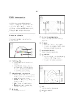
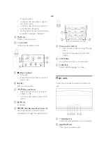
Page 12: ...s Color buttons Color buttons Select tasks or options for Blu ray discs or SmartTV services DISC Switch to disc source DOCK for iPod Switch to Philips dock for iPod or iPhone HELP Access the onscreen help SOURCE Select an audio input source or radio source c Home Access the home menu a POP UP MENU DISC MENU Access or exit the disc menu when you play a disc b BACK Return to a previous menu screen I...

Page 13: ...p to the previous or next track FKDSWHU RU ÀOH In radio mode select a preset radio station d Pause Pause play e Fast Backward Fast Forward Search backwards or forward Press repeatedly to change the search speed a Alphanumeric buttons Enter values or letters using SMS style entry In radio mode select a preset radio station b TOP MENU Access the main menu of a video disc c SUBTITLE Select subtitle l...

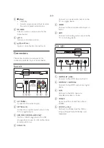
Page 14: ...NLY Slot for a USB storage device The USB storage device is used to rent online videos and access BD Live d COAX IN c d f e a b Connect to a coaxial audio output on the TV or a digital device e VIDEO Connect to the composite video input on theTV f AUX Connect to an analog audio output on the TV or an analog device Rear right a HDMI OUT ARC Connect to the HDMI input on theTV b HDMI IN1 HDMI IN2 Con...

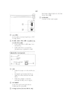
Page 15: ...odels Subwoofer connectors a LED When the power is on the LED turns on During pair up between the home theater and the subwoofer the LED blinks When the wireless connection succeeds the LED turns on again b CONNECT Press and hold to pair up the home theater and the subwoofer c 9ROWDJH VHOHFWRU RU VLD 3DFLÀF RQO a b b a d c Switch the voltage selector to the local power line voltage d AC MAINS Conn...

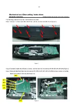
Page 16: ...p 1 Remove 11 screws around the bottom Cover and then remove the bottom Cover Figure 1 Step 2 Dismantle Amplifier Board Remove 2 screws and then disconnect connectors XP1 XP5 XP4 XP3 XP8 XP2 Figure 2 Figure 2 Step 3 Dismantle Main Board Disconnect connectors XP1 XP19 P4 XP7 XP17 XP16 P6 XP20 remove 4 screws on the Main Board and 5 screws on the back pannel Figure 2 3 XP1 XP5 XP4 XP3 XP8 XP2 ...

Page 17: ...et Figure 3 Step 4 Dismantle IN Board Disconnect connectors XP1 XS609 remove 1 screw on the IN Board and 2 screws on the back Figure 4 pannel Figure 4 Figure 5 Step 5 Dismantle VFD Board Disconnect connector XP6 and then remove 4 screws Figure 5 3 2 XP8 XP1 XP18 XS1 XP19 P4 XP7 XP17 P6 XP16 XP3 XP20 XP1 XS609 XP6 ...

Page 18: ... loader Figure 6 Figure 6 Step 8 Dismantle Power Board Remove 2 screws disconnect connectors CN504 CN501 and then remove the Power Board Figure 7 Step 9 Dismantle IN Board Disconnect connectors XP1 XS609 remove 1 screw and then remove the IN Board Figure 7 Figure 7 Step 7 Dismantle Key Board Remove 5 screws disconnect connector XS1 and then remove the Key Board Figure 6 XS1 XP1 XS609 CN504 CN503 P...

Page 19: ...ormation please refer to the model set Figure 8 Figure 9 Step 10 Dismantle the cover of speakers FInish Step1 to Step9 first then remove 12 screws on the back pannel and 2 screws on the bottom Figure 8 Open the Front cover remove 16 screws on the cover of speakers Figure 9 3 4 ...

Page 20: ...he Back pannel Figure 1 Figure 1 Step2 Before remove the back pannel disconnect the connector XP6 Figure 2 Step3 Step4 Dismantle Amplifier Board first disconnect 3 connectors XP3 XP5 XP11 then remove 4 screws Figure 2 Dismantle Powerl Board first disconnect connector CN501 then remove 4 screws Figure 2 Step5 Dismantle Wifi Board remove 2 screws Figure 2 3 5 XP6 XP3 XP5 XP4 XP11 CN503 CN501 ...

Page 21: ...ce you start upgrade pls don t power off the DUT after upgrade DUT will restart up later a moment time or you press button OK on remote control 2 Check the version information after upgraded Wake up DUT select Setup Advance version information you will see a interface as below Model HTB5XXX XX Software version System SW 1 04 00 Subsystem SW 00 17 00 00 4 1 3 Factory Reset Steps Press Home button o...

Page 22: ...N2 3 4 No Yes Yes Yes Correct connection No Yes Replace U135 or VFD Check every supply voltage on Main Board whether normal or not XP8 PIN2 24V PIN3 12V PIN4 3 3V Check voltage 24V 12V 3 3V on Power Board at CN504 position and Front Control Board at XP6 PIN9 24V PIN8 12V Check the power key SW1 open closed key SW3 source key SW2 stop key S606 on Front Board whether work normally or not Check Front...

Page 23: ...e connection XS1 to XP1 on Main Board Yes Replace U36 on Main Board or replace Main Board No Yes Replace switch on keypad Board Check voltage 3 3V on keypad board XS1 of pin 2 3 4 Check keypad Board signals of XS1 pin2 3 4 5 whether normal or not if have high or low voltage ...

Page 24: ... work Go No Replace the battery for remote control Yes Check the 3 3V net on Front Control Board to Main Board XP8 PIN8 No Yes Replace IR1 Check battery of remote control whether exhausted or not Check power supply of IR1 on Front Control Board whether normal or not IR1 Pin1 3 3V ...

Page 25: ...k voltage 33 5V 33 5V for HTB5150D for whether normal or not at on Amplifier Board Check the 24Pin FFC connection XP11 on Main Board and XP1 on Amplifier Board whether right or not between Main Board and Amplifier Board Check the control signal whether right or not at the XP11 all pin voltage and signal Check CN504 Pin 1 33 V PIN 8 3 3V on power Board whether normal or not on main board ...

Page 26: ...le shooting Chart No video output No video output Go Add L457 R188 Yes No No Replace Main IC or Main Board Check L457 R188 whether right on Main Board Check the video signal whether right at U4 PIN 6 on IN board ...

Page 27: ...open the disk door Can t read disc or can t open the disk door Go Check XP16 on Main Board No Yes Fix 45Pin 8Pin 4Pin cable No Replace Loader Yes Check loader work normally or not Check 45Pin 8Pin 4Pin cable from Main Board to Loader connect right or not ...

Page 28: ...No Change the Tuner IC U184 No Yes Yes No Yes Replace main Board Check Main Board U36 power supply circuit Check voltage 3 3V at Tuner module U184 Pin11 whether right or not Check Tuner U184 module PIN2 and Pin20 normal or not Check voltage at XS1 pin2 5V on Main Board whether normal or not Check the U184 PIN9 PIN13 I2C output on Main Board normal or not ...

Page 29: ...s Check AUX IN connector No Yes Replace main board Check aux in Board No Yes Check voltage at U185 PIN36 3 3V on Main Board whether normal or not Check Main Board U185 pin11 pin12 signal input whether right or not Refer to Power Board CN504 No Check Main Board XP11 all pin signal input whether right or not ...

Page 30: ...n Board to Amp connector No Yes No Yes Check signal at JACK601 PIN3 MP3_R PIN2 MP3_L ON front board whether normal or not Check Main Board U185 CS5346 PIN7 PIN8 L R signal input right or not Check voltage at U185 PIN36 3 3V on Main Board whether normal or not Refer to MAIN Board U5 PIN6 and Refer to Power Board CN504 Check Main Board XP11 all pin signal input whether right or not ...

Page 31: ...r to Power Board CN504 Yes Check Coax in Board C18 L1 No Replace U22 CS8422 Check Main Board Yes Yes No Check voltage at U22 PIN3 PIN22 3 3V on Main Board whether normal or not Check Main Board U22 CS8422 PIN2 input signal whether normal or not Check U22 CS8422 whether broken or not ...

Page 32: ...5 11 Trouble shooting Chart wifi in does not work Go No Check netting twine link normal or not Yes Check P1 Pin2 Pin3 Pin5 Pin6 from netting twine normal or not Replace P1 W I FI does not work ...

Page 33: ... Check XP21 of main board whether normal or not Yes Check power supply No Yes Check the optical connector Fix XS3 Check pin1 of P2 on optical in Board Pin1 3 3V whether normal or not Check the input signal of U22 CS8422 whether normal or not Check the voltage clock and data of U22 Yes ...

Page 34: ... No No sub output Go Check power supply Yes No Yes Check the voltage clock and data of U4 and U1 Check U4 and wireless module Check the SUB AMP board xp11 of PIN10 33 5V PIN4 12V PIN2 5V Check U1 TAS5538 pin of I2S signal whether normal or not ...

Page 35: ... 1 0 1 5 3 0 1 1 E 2 1 5 6 6 6 86 5 1 237 1 03 1 63 0 1 7 6 7 5 5 9 5 73 ROORZ GHVLJQ E 3520 LQH 1 6 5 E E 6 6 1 6 3 6 6 1 6 B 0 6 03 HFRGHU 07 3520 E 9 5 5 321 2 5 8 57 5 17 1HZ GHVLJQ 03 8 2 352 6625 7 6 5 0 2XWSXW 0 1 0 1 5 5 7 7 ORFN LDJUDP UDIW RU 0DLQ 5 3520 E B 0 0 63 0 6 1 6 1 ...

Page 36: ... 7 7 ORFN LDJUDP UDIW RU 68 0 8 0 ODVK 32 5 6833 9 9 9 1 0 1 5 3 0 6 63 7 6 3 7 5 ROORZ GHVLJQ 6 1 6 17 1HZ GHVLJQ 8 2 352 6625 7 6 3 1 68 6 2 6 2 ...

Page 37: ... 32 5 6RXUFH 23 1 26 32 5 6285 23 1 26 6 7 6 7 S 9 13 S 9 13 6 7 6 7 6 7 6 7 6 7 6 7 S 9 13 S 9 13 6 7 6 7 6 3 1 PP PP 6 3 1 PP PP 6 7 6 7 6 7 6 7 S 9 13 S 9 13 S 9 13 S 9 13 KEY Board Circuit Diagram for HTB5150D 12 Soundbar 7 1 7 1 ...

Page 38: ...OO 6 3 1 PP PP 6 3 1 PP PP 3 6 9 6 S 3 6 9 6 S 3 3 1 PP 3 3 1 PP X 9 5 X 9 5 3 63 B 1 237 3 63 B 1 237 9 9RXW 3 6 9 6 S 3 6 9 6 S 5 5 5 5 5 5 X 9 9 X 9 9 X 9 9 X 9 9 S 9 13 S 9 13 X 9 5 X 9 5 X 9 5 X 9 5 5 5 86 B7HVW 86 B7HVW X 9 9 X 9 9 X 9 5 X 9 5 S 9 13 S 9 13 S 9 13 S 9 13 P P 86 B7HVW 86 B7HVW 1 X 9 1 X 9 1 S 9 13 1 S 9 13 IN Board Circuit Diagram for HTB5150D 12 Soundbar 7 2 7 2 ...

Page 39: ...5 5 5 5 5 5 5 5 P P X 9 9 X 9 9 5 5 X 9 9 X 9 9 4 131B 0 4 131B 0 00 9 9 00 9 9 5 5 5 9 5 9 5 5 X 9 X 9 5 5 5 5 3 3 1 PP 607 3 3 1 PP 607 5 5 P P X 9 X 9 X 9 5 X 9 5 9 9 3 3 3 1 3 3 3 1 3 13 1 3 3 13 1 3 3 3 3 3 5 5 5 5 X 9 5 X 9 5 5 5 5 5 P P 5 5 8 5 9 5B9 B 6 1 8 5 9 5B9 B 6 1 6 6 6 6 6 RXW 6 LQ 1 6 6 9 6 6 6 6 6 6 6 6 6 6 6 6 9 6 6 6 6 9 1 26 5 5 5 5 5 5 5 50B PP 5 50B PP 5 1 9 1 1 4 131B 0 4 1...

Page 40: ...1500uF 16V CE510 1500uF 16V CE510 R552 470 R552 470 R577 680 R577 680 1000uF 16V CE511 1000uF 16V CE511 C549 100pF 1KV C549 100pF 1KV R516 22K R516 22K C543 0 1uF 50V X7R C543 0 1uF 50V X7R C535 1000pF 50V X7R C535 1000pF 50V X7R R569 NC R569 NC D511 BYV26C 1A 600V D511 BYV26C 1A 600V R507 22 R507 22 R539 100 R539 100 C530 0 22uF 50V X7R C530 0 22uF 50V X7R R503 1M R503 1M 470uF 200V CE501 470uF 2...

Page 41: ...1 1 1 39 B 39 B 1 0 0 X 9 9 X 9 9 5 5 5 5 3 3 1 PP 3 3 1 PP S 9 5 S 9 5 3 3 1 PP 3 3 1 PP X 9 5 X 9 5 4 313B 0 4 313B 0 X 9 5 X 9 5 X X 73 73 X 9 5 X 9 5 S 9 5 S 9 5 X 9 X 9 5 5 X 9 5 X 9 5 X 9 5 X 9 5 X 9 9 X 9 9 1 X 9 5 1 X 9 5 0 0 X 9 X 9 73 73 X 9 X 9 X 9 5 X 9 5 S 9 13 S 9 13 S 9 5 S 9 5 5 5 X 9 5 X 9 5 X X X 9 5 X 9 5 1 X 9 5 1 X 9 5 X 9 5 X 9 5 X 9 5 X 9 5 5 5 73 73 5 5 1 X 9 9 1 X 9 9 73 7...

Page 42: ... 5 5 X 9 X 9 73 73 5 5 X 9 9 X 9 9 73 73 5 5 73 73 5 5 X 9 9 X 9 9 5 5 5 5 5 5 X 9 X 9 5 5 5 5 73 73 4 313B6 4 313B6 73 73 5 5 X 9 5 X 9 5 73 73 5 5 73 73 73 73 1 S 9 13 1 S 9 13 73 73 1 X 9 5 1 X 9 5 73 73 X 9 X 9 1 1 5 1 5 1 5 5 5 5 73 73 X 9 5 X 9 5 5 5 X 9 5 X 9 5 X 9 9 X 9 9 5 1 5 1 5 5 5 5 73 73 73 73 1 X 9 5 1 X 9 5 5 5 5 5 8 7 6 8 7 6 3 0B 30B 3 0B 33B 3 0B 30B5 3 0B 33B5 966 3 B 70 3 B 73...

Page 43: ... 9 8 7 8 7 9 5 1 1 3 1 9 1 73 5 5 X 9 9 X 9 9 5 5 X 9 9 X 9 9 5 5 X 9 9 X 9 9 8 2B 8 2B 32 9 1 9 1 933 1 92 1 73 X 9 9 X 9 9 X 9 9 X 9 9 X 9 9 X 9 9 X 9 9 X 9 9 5 5 X 9 5 X 9 5 X X X 9 5 X 9 5 5 5 5 5 X 9 5 X 9 5 X 9 5 X 9 5 5 5 5 5 4 313B 0 4 313B 0 X 9 9 X 9 9 4 131B 0 4 131B 0 X 9 9 X 9 9 X 9 9 X 9 9 X 9 9 X 9 9 5 N 5 N 5 5 9 9 9 9 5 5 5 5 5 5 5 5 5 5 X 9 X 9 X 9 9 X 9 9 5 5 X 9 9 X 9 9 5 5 X 9...

Page 44: ...X 9 5 5 X 9 9 X 9 9 X 9 9 X 9 9 X 9 9 X 9 9 X 9 9 X 9 9 73 73 73 73 X 9 9 X 9 9 X 9 9 X 9 9 73 73 X 9 9 X 9 9 51 51 X 9 9 X 9 9 5 5 5 5 X 9 9 X 9 9 5 5 73 73 73 73 X 9 9 X 9 9 5 5 X 9 9 X 9 9 73 73 X 9 9 X 9 9 51 51 X 9 9 X 9 9 73 73 X 9 9 X 9 9 X 9 9 X 9 9 8 07 B B 3B B 8 07 B B 3B B 59 2 59 2 0 59 2 59 2 59 2 59 2 9 B0 03 966 B0 03 73B0 03 71B0 03 1 B 0 1 B 1 B 1 B 59 2 8 59 2 5 4 5 4 5 4 5 4 5 ...

Page 45: ...B 1 1 B 4 1 B 95 0 1 B 0 7 1 B 7 966B 0 966B 0 966B 3 966B 3 966B 7 966B 7 9 B 1 9 B 5 9 B 5 X 9 9 X 9 9 X 9 9 X 9 9 X 9 9 X 9 9 X 9 9 X 9 9 5 5 X 9 9 X 9 9 X 9 9 X 9 9 X 9 9 X 9 9 X 9 9 X 9 9 X 9 9 X 9 9 X 9 9 X 9 9 73 73 73 73 X 9 9 X 9 9 X 9 9 X 9 9 X 9 9 X 9 9 5 5 X 9 9 X 9 9 5 5 S 9 13 S 9 13 73 73 X 9 9 X 9 9 X 9 9 X 9 9 X 9 9 X 9 9 8 07 B B 3B B 8 07 B B 3B B 9 B 9 B 9 B 9 B 9 B 9 B 59 0 9 ...

Page 46: ...B 5 X 9 9 X 9 9 9 9 X 9 5 X 9 5 X 9 9 X 9 9 0 1 0 1 5 5 8 8 5 5 S 9 13 S 9 13 X 9 9 X 9 9 X 9 9 X 9 9 X 9 5 X 9 5 73 73 5 1 5 1 X 9 9 X 9 9 1 1 X 9 9 X 9 9 5 5 73 B75 1 73 B75 1 5 5 S 9 13 S 9 13 5 5 5 1 5 1 S 9 13 S 9 13 X 9 9 X 9 9 X 9 X 9 73 B 2 73 B 2 73 B 73 B 5 5 8 6 8 6 LQSXW 9RXW 1 RXWSXW 73 B 2 73 B 2 S 9 13 S 9 13 X 9 5 X 9 5 S 9 13 S 9 13 X 9 5 X 9 5 5 5 5 5 3 3 1 PP 3 3 1 PP 5 5 X 9 9 ...

Page 47: ...3 S 9 13 73 B75 73 B75 B B 0 B 9 0 B 9 5 5 X 9 9 X 9 9 1 1 1 1 2B 2B 5 5 X 9 9 X 9 9 5 5 5 5 8 07 B B 3B B 8 07 B B 3B B 26 1 02 16 16 16 02 02 7 2 752 22 75 3 0 02 02 2 2 2 2 2 2 2 02 2 2 2 9 B 9 B 1 B 1 B 9 B 9 B 1 B 1 B 8 9 9 2 9 2 03 287 03 287 03 287 7B 75 287B 75 1B 567 1 B 9 95 9 75 1 75 1 75 1 75 1 1 1 1 1 1 1 1 1 3 2 3 2 9 5 1 5 3 5 1 5 3 5 4 02 02 1 1 5 1 5 1 5 5 1 S 9 5 1 S 9 5 9 B3 9 B...

Page 48: ... 5 21 8 1DQGB EB0 5 21 1 1 1 1 1 6 5 5 1 1 9 966 1 1 3 1 1 1 1 1 1 1 1 1 2 2 2 2 1 1 1 966 9 1 1 1 2 2 2 2 1 1 1 1 73 73 P P 5 5 5 1 5 1 1 1 1 X 9 9 1 X 9 9 1 1 8 07 B B 3B B 8 07 B B 3B B 9 B 2B67 9 B 2B67 9 B 2 966 B 2 8 5 8 7 967 9 7 9 5 5 23 56 5 6 7B 9 B 2 3 2 1 1 1 1 1 5 1 1 5 1 1 1 1 1 1 5 1 1 1 1 1 1 1 1 1 0 2 0 3 2 1 1 1 1 X 9 9 X 9 9 5 5 1 1 5 5 X 9 9 X 9 9 5 1 5 1 5 5 5 5 X 9 9 X 9 9 5 ...

Page 49: ... 13 S 9 13 5 5 5 5 P P 4 131B 0 4 131B 0 5 5 X 9 9 X 9 9 5 5 5 5 1 S 9 13 1 S 9 13 1 S 9 13 1 S 9 13 5 5 X 9 X 9 0 330 0 330 4 131B 0 4 131B 0 5 5 X 9 X 9 1 S 9 13 1 S 9 13 5 5 5 5 5 5 1 S 9 13 1 S 9 13 5 5 3 3 1 PP 3 3 1 PP 5 5 S 9 13 S 9 13 5 5 5 P 5 P 5 5 S 9 13 S 9 13 X 9 9 X 9 9 5 5 5 5 P P S 9 13 S 9 13 X 9 9 X 9 9 5 5 5 5 5 5 5 5 1 7 1 7 1 S 9 13 1 S 9 13 5 0 5 0 70 70 1 S 9 13 1 S 9 13 X 9...

Page 50: ...2 X 9 9 X 9 9 1 1 1 S 9 1 S 9 5 5 1 1 5 1 5 1 X 9 9 X 9 9 X 9 9 X 9 9 3 2 3 2 3 21B 3B 1 6 3 21B 3B 1 6 5 5 3 2 3 2 86 B7HVW 86 B7HVW 5 1 5 1 X 9 9 X 9 9 3 2 3 2 3 2 3 2 X 9 9 X 9 9 X 9 5 X 9 5 1 1 3 2 3 2 3 2 3 2 X 9 9 X 9 9 X 9 9 X 9 9 5 1 5 1 X 9 9 X 9 9 3 21B 3B 1 6 3 21B 3B 1 6 4 313B3 66 7 4 313B3 66 7 5 1 5 1 8 3 60 8 3 60 5 75 5 1 1 7 77 7 7 3 7 7 7 1 1 1 5 3 5 7 5 1 5 5 3 2 3 2 8 07 B B 3...

Page 51: ... 6 7 72 5 6 6 1 3 2 3 2 3 2 9B5 9 B 7 1 9 6 287 26 2 5 7 0B 1 6 287 26 2 5 3 2 50 567 1 X 9 X 9 5 5 S 9 13 S 9 13 S 9 13 S 9 13 5 5 5 5 8 6 8 6 6 287 6 6 1 9 567 1 1 1 1 1 1 1 9 7 7 94 94 7 1 1 0 1 1 0 1 1 1 0 6 1 1 3 287 3 287 1 1 1 1 1 1 9 6 1 1 1 1 6 287 6 5 0 1 9 17 29 73 73 5 5 5 5 S 9 13 S 9 13 Q P Q P 5 5 73 73 S 9 13 S 9 13 5 5 5 5 X 9 9 X 9 9 X 9 X 9 5 5 5 5 5 0 5 0 1 S 9 13 1 S 9 13 3 3 ...

Page 52: ... 9 00 9 9 8 8 5 5 5 5 1 X 9 1 X 9 6 6 73 73 5 5 X 9 9 X 9 9 X 9 9 X 9 9 70 70 5 5 X 9 X 9 X 9 X 9 X 9 9 X 9 9 S 9 5 S 9 5 73 73 5 5 X 9 5 X 9 5 73 73 5 5 5 5 5 1 5 1 5 5 5 5 5 5 S 9 13 S 9 13 8 8 X 9 9 X 9 9 5 1 5 1 32 B B 32 B B XGLRB5 7 XGLRB 1 XGLRB 1 1 1 9 9 6 5 1 B9 S 9 13 S 9 13 5 5 5 1 5 1 X 9 5 X 9 5 5 5 S 9 5 S 9 5 5 5 5 5 5 5 73 73 1 S 9 13 1 S 9 13 S 9 13 S 9 13 5 5 4 1 131B 0 4 1 131B ...

Page 53: ...520B EB0 8 3520B EB0 1 1 1 1 6 6 3 9 5 5 5 5 0 0 5 1 5 1 5 1 5 1 5 5 1 1 1 S 9 13 1 S 9 13 5 5 6 6 1 S 9 13 1 S 9 13 5 5 5 1 5 1 5 1 5 1 5 5 5 5 5 5 5 5 4 131B 0 4 131B 0 796 UUD V 6 3 6 B73 6 796 UUD V 6 3 6 B73 6 1 1 5 1 5 1 796 UUD V 6 3 6 B73 6 796 UUD V 6 3 6 B73 6 1 1 0 3 0 3 4 1B 6 4 1B 6 6 7 7 4 1B 6 4 1B 6 6 5 5 6 6 6 6 X 9 9 X 9 9 4 131B 0 4 131B 0 5 5 1 1 1 S 9 13 1 S 9 13 5 1 5 1 X 9 9...

Page 54: ...3 73 1 1 S 9 13 S 9 13 5 5 X 9 9 X 9 9 1 X 9 1 X 9 X 9 9 X 9 9 73 73 8 8 9 B9 B 9 966 B9 B 8 9 B9 B 7 966 B9 B 7 9 B3 3 966 B3 3 16B 7 16B 7 2 20 2 2 5 26 7 26 7 087 9 B287 8 9 5B287 9 B287 9 9 B287 8 9 B 966 B 5 26 7 26 7 26 7 237 0 1 63 7 2 5 63 B3 B0 B3 B0 B3 B0 B3 B0 9 B 0 966 B 0 0 9 B 0 B 9 B 0 B 0 6 0 6 73 1 1 5 0 5 0 1 1 6 6 5 5 5 5 1 1 60 60 6 6 5 5 5 5 0 330 0 330 3 0 3 0 5 1 0 5 1 0 1 1...

Page 55: ...5 1 73 73 73 73 5 1 5 1 73 73 5 5 73 73 73 73 73 73 73 73 73 73 73 73 73 73 5 5 73 73 73 73 5 5 5 5 73 73 73 73 73 73 73 73 73 73 73 73 73 73 8 07 B B 3B B 8 07 B B 3B B 9287 9287 9287 9 9287 5 9287 8 9287 7 9287 8 9287 3 9287 3 9287 3 9287 3 928796 1 9287 6 1 9287 3 5 5 73 73 Main Board Circuit Diagram for HTB5150D 12 CVBS 7 19 7 19 ...

Page 56: ... 3 86 3 86 9 1 6KHOO 6KHOO X 9 9 X 9 9 5 5 5 5 5 5 6 3 6 9 6 S 6 3 6 9 6 S 4 1 313B 0 4 1 313B 0 5 5 X 9 9 X 9 9 S 9 13 S 9 13 S 9 13 S 9 13 P P 5 5 5 5 X 9 9 X 9 9 S 9 13 S 9 13 S 9 13 S 9 13 5 5 4 131B 0 4 131B 0 5 5 8 8 6 3 6 9 6 S 6 3 6 9 6 S 5 5 5 5 X 9 X 9 5 5 5 5 X 9 9 X 9 9 6 3 1 PP PP 6 3 1 PP PP 8 8 X 9 9 X 9 9 X 9 9 X 9 9 4 1 313B 0 4 1 313B 0 5 5 USB MIC Board Circuit Diagram for HTB51...

Page 57: ... C532 1000pF 50V X7R 22uF 35V CE515 22uF 35V CE515 R502C 1M R502C 1M 100uF 400V CE5011 100uF 400V CE5011 C540 0 01uF 400V C540 0 01uF 400V JP504 JP504 R536 680 R536 680 C522 100pF 1KV C522 100pF 1KV R572 10 R572 10 JMP27 0 JMP27 0 R576 10K R576 10K LIF501 LIF501 R527 470K R527 470K CY503 NC CY503 NC C535 0 1uF 50V X7R C535 0 1uF 50V X7R 4 7uF 16V CE516 4 7uF 16V CE516 C528 0 047uF C528 0 047uF R52...

Page 58: ...5 X 9 9 X 9 9 4 3B 4 3B 6 X 9 9 X 9 9 X 9 9 X 9 9 X 9 9 X 9 9 5 5 4 131B 0 4 131B 0 5 5 X 9 X 9 X 9 9 X 9 9 X 9 9 X 9 9 X 9 X 9 X 9 9 X 9 9 5 5 5 5 4 131B 0 4 131B 0 X 9 9 X 9 9 X 9 9 X 9 9 X 9 9 X 9 9 X 9 9 X 9 9 5 5 5 5 5 5 4 3B 4 3B 6 5 5 8 8 9LQ 9VV 1 9RXW 5 5 Amplifier Board Circuit Diagram for HTB5150D 12 Subwoofer POWER 7 22 7 22 ...

Page 59: ... 5 5 73 73 S 9 13 S 9 13 5 5 4 131B 0 4 131B 0 P P 5 5 73 73 3 3 1 00 3 3 1 00 5 5 5 5 3 3 5 5 5 5 5 5 5 5 73 73 73 73 73 73 5 5 73 73 S 9 5 S 9 5 73 73 S 9 13 S 9 13 5 0 5 0 5 5 1 X 9 9 1 X 9 9 5 1 5 1 X 9 9 X 9 9 5 5 S 9 13 S 9 13 5 5 8 0 1 8 0 1 026 B 0 62B 63 567 5 966 7 67 0 6 7 6 3 0 2 5 7 7 966 2B 3 3 0 3 0 3 0 3 0 3 0 3 0 3 0 3 0 3 0 6 B B 7 63 0 62B 026 B 63 66 3 0 576 76 576 76 9 9 7 7 5...

Page 60: ... PP 3 3 1 PP X X X 9 5 X 9 5 X 9 5 X 9 5 X 9 5 X 9 5 S 9 5 S 9 5 5 5 S 9 13 S 9 13 P P X 9 5 X 9 5 5 5 5 5 5 5 4 313B 0 4 313B 0 73 73 X 9 5 X 9 5 X 9 X 9 X 9 5 X 9 5 1 X 9 9 1 X 9 9 X 9 5 X 9 5 5 5 X 9 X 9 X 9 5 X 9 5 5 5 4 131B 0 4 131B 0 73 73 5 5 5 5 5 5 X 9 5 X 9 5 S 9 13 S 9 13 X X X 9 5 X 9 5 5 5 8 03B 3B7 6 8 03B 3B7 6 9 B 27 6 3 0B 5 6 7B 3 0B 2 B 1 1 95 0 0 0 3 0B 5 6 7B 3 0B 9 B 9 B 67B...

Page 61: ...B5 3 0B 33B5 966 3 B 70 3 B 73 95B 1 9 6 B 02 0 26 B5 6 966 B 25 9 B 25 02 5 6 7 3B6 3 1 087 6 6 5 6 6 1 6 1 6 1 6 1 95B 6 287 6 2 5 2 7 67 369 1 B 55 9 B 25 966 B 25 9 3 0B0B 3 0B3B 3 0B0B 3 0B3B 3 0B0B 3 0B3B 3 0B0B 3 0B3B 3 0B0B 3 0B3B 3 0B0B 3 0B3B 9 B3 0 966B3 0 95B3 0 3 0B0B 3 0B3B 3 0B0B 3 0B3B 5 5 1 1 1 1 5 5 5 5 X 9 5 X 9 5 5 5 5 1 5 1 P P 8 8 X 9 9 X 9 9 5 5 4 1 131B 0 4 1 131B 0 5 5 X 9...

Page 62: ...Key Board Print layout bottom side for HTB5150D 12 Soundbar 7 26 7 26 ...

Page 63: ...Power Board Print layout bottom side for HTB5150D 12 Soundbar 7 27 7 27 ...

Page 64: ...IN Board Print layout top side for HTB5150D 12 Soundbar 7 28 7 28 ...

Page 65: ...IN Board Print layout bottom side for HTB5150D 12 Soundbar 7 29 7 29 ...

Page 66: ...FV Board Print layout top side for HTB5150D 12 Soundbar 7 30 7 30 ...

Page 67: ...FV Board Print layout bottom side for HTB5150D 12 Soundbar 7 31 7 31 ...

Page 68: ...Amplifier Board Print layout top side for HTB5150D 12 Soundbar 7 32 7 32 ...

Page 69: ...Amplifier Board Print layout bottom side for HTB5150D 12 Soundbar 7 33 7 33 ...

Page 70: ...Main Board Print layout top side for HTB5150D 12 Soundbar 7 34 7 34 ...

Page 71: ...Main Board Print layout bottom side for HTB5150D 12 Soundbar 7 35 7 35 ...

Page 72: ...Power Board Print layout bottom side for HTB5150D 12 Subwoofer 7 36 7 36 ...

Page 73: ...Amplifier Board Print layout top side for HTB5150D 12 Subwoofer and USB Board for Soundbar 7 37 7 37 ...

Page 74: ...Amplifier Board Print layout bottom side for HTB5150D 12 Subwoofer and USB Board for Soundbar 7 38 7 38 ...

Page 75: ... 7 1 6B 7 1 6B 1 1 1 6B0 9 B 9 1 9 9 6 9 9 6 7 1 1 9 03B087 1 03B567 9 9 9B 1 3 URP 0DLQ RDUG RQQHFW WR URQW 86 9B 9 B 3LQ 1R 3LQ VVLQ 1 86 B9 32 5B 7 1 3B6 86 0 27 86 3 3 1 1 B 55 3 URP 0DLQ RDUG RQQHFW WR UHDU 86 3LQ 1R 3LQ VVLQ 86 B9 1 86 0 86 3 5HPDUNV 9 KLJK VSSHG GLIIHUHQFH 5HPDUNV 9 KLJK VSSHG GLIIHUHQFH 6 9 9 9 6 9 9 5HPDUNV 5HPDUNV 5HPDUNV 9 63 63 63 5HPDUNV 9 3 URP 0 1 RDUG RQQHFW WR 6 P...

Page 76: ...1 Pin20_POWER_derating XP11 Pin12_ AMP MUTE XP11 P13_AMP RST XP11 P9_ AMP SCL XP11 Pin4_AOSDATA2 XP11 Pin B BAOMCLK XP11 Pin10_AMP SDAXP11 Pin5_AOBCK XP11 Pin10_AMP SDAXP11 Pin5_AOBCK XP11 Pin10_AMP SDAXP11 XP11 Pin10_AMP SDA XP11 Pin5_AOBCK ...

Page 77: ...8 3 8 3 Waveforms for measure point XP11 Pin2_LRCK XP11 Pin23_PDWN XP11 Pin22_OTW XP11 Pin1_AOSDATA0 XP11 Pin3_AOSDATA1 ...

Page 78: ...400MHz AudioDSPx3 Mali 400 MP HDMI TX RX 1 4 Ethernet SATA OPU DDR3 384MB NAND 1GB USB 2 0 2 CH audio 7 1 CH audio HDMI 1 4 Component CVBS Ethernet Audio DAC S PDIF DVO Motor Driver HDMI 1 4 DVI 9 1 U1 Main IC MT8580 BDAGO Funtion Block Diagram ...

Page 79: ...Exploded View of HTB5150D 12 Soundbar 10 1 10 1 ...

Page 80: ...Exploded View Of HTB5150D 12 Subwoofer 10 2 10 2 ...

Page 81: ...REVISION LIST Version 1 1 11 1 To remove the UART and JTAG port from Main Board schematics to comply with DRM security agreement and Vernace Audio Watermarking ...

Reviews: