


10-9
10-9
+
-
+
-
VDD
STB
D
1
EN1
SRG8
M
M
9
10
11
12
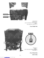
CAROUSEL-MOTOR
delay circuitry
PORE
C
D
E
F
voltage stab.
D
3
1
2
3
4
5
6
7
8
9
10
11
12
13
14
15
1
2
3
4
5
6
7
8
2873 D6
2875 E6
2876 C7
2877 F11
SILD
DRAWER-MOTOR
board
GND
SHR_STR
2
5.6V v
ersion only
GNDA
13
14
15
A
B
C
D
E
F
G
H
A
B
3714 F8
3715 G8
3716 B3
3717 B3
1882
mainboard
(19 Pin)
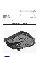
3CDC-LLC
D
D
1883
2852 H2
2853 G4
2854 B3
2858 A9
2860 A11
2861 B11
2862 B8
2863 B8
2864 B3
2865 C4
2867 A8
2872 G10
3750 B7
3751 C7
3752 A6
3753 A6
3V-5V log. Level
DIG.
OUT
POS rec
FE-ST-VK-N
LEFT
DIPMATE
1
from digital-out circuitry
SD
A
to 7877 on part 1
DOWN
1
2878 F11
2881 F8
2882 B10
2893 F12
3700 H2
3705 G4
3706 G4
3707 G4
3708 H4
3711 G5
3712 B4
3713 G8
3876 C11
3877 F12
3878 E12
3879 D7
3
RF-500TB
RF-500TB
1876
2
changer control
GND
COAX2/EBU
DRIVE UP/
3718 G3
3730 G2
3731 G2
3732 G2
3733 G2
3734 H2
3740 A7
3741 A7
3742 B7
3743 B7
3744 A9
3746 B10
MP724 D8
MP725 D8
MP726 D8
MP740 H14
to/from 7877 on part 1
3809 B2
3814 D12
3831 G4
3851 D7
3858 A11
3859 B11
3860 B7
3861 B8
3864 A7
3865 A10
3866 A10
3868 B10
3869 B10
3871 F12
3872 C13
3874 C13
3875 C12
MP811 F14
MP822 E3
MP823 E3
MP824 D4
BASIC VERSION
COAX1/+3V
6871 F8
6872 E8
6873 E8
6874 G7
6875 F7
6876 D13
6877 D12
6878 E8
6879 G4
7805-A B9
7805-B A8
7812 G8
7871 C5
7873 D10
7874 C12
7875 D12
7876 G3
MP721 C8
MP722 E8
MP723 D8
MP886 G3
MP887 H5
MP888 G5
MP889 G5
FR
OM 7877 ON P
A
R
T
1
SHR_CL
3.2V
SICL
5V1
MP741 G14
MP742 G14
MP801 E12
MP803 F10
MP804 G14
MP805 F13
MP806 F13
MP807 F14
MP808 F13
MP810 F13
4803 B4
4811 A7
4812 B7
4876 D13
5802 B4
+5V(+5.6V)
DATA
GND
MP825 D4
MP830 A7
MP832 G9
MP833 F14
MP835 F14
MP854 A13
MP856 E14
MP857 B13
MP863 C11
MP865 D11
MP866 E8
MP867 E8
MP868 F8
MP869 C12
MP871 D6
MP874 D12
MP881 G2
MP882 G2
EBU_GND
5
8003
Transformer
1877
#
#
#
3880 E6
3881 E7
3882 D7
3883 D6
3884 D6
3885 D6
3886 E7
3887 D6
3888 F12
3890 F11
3891 F11
3893 F11
3898 F7
3899 D12
3905 C5
4
D
logic
(15 Pin)
0V
G
H
1805 E15
1875 D2
1878 E2
1880 F8
1881 E8
2829 D6
2830 C9
2831 B9
2832 A8
Output enable
+10V
GND
part 2
MP890 B3
MP891 B5
MP892 B5
MP897 E13
MP898 E13
MP899 E14
0V
to combi-
D
TRAY POS
8002
SW_INFO
POS1 rec
RIGHT
EBUGND
2860
10u
2878
220p
3874
10K
3858
47K
1K
3891
BAS216
6876
1880
10K
3878
9
12
5
3
4
8
11
15
7871
TDA7073A
14
10
2
1
6
7
16
13
OUT1-
220R
3898
1
2
3
4
5
GNDA
1875
FE-ST-VK-N
220R
3887
47p
2877
3744
10K
3741
22K
7875
BC847B
3899
100R
3R3
3851
4811
3872
10K
2867
220p
3746
10K
3860
220p
2862
3715
100K
10K
22K
3713
3879
100K
2858
220u
470R
3893
10K
3714
3742
22K
220p
2893
BC847B
7812
8
4
TDA1308T
7805-A
3
2
1
BAS216
6871
1K
3750
13
12
11
9
10
1
16
8
HEF4094BT
7873
3
2
15
4
5
6
7
14
10K
3877
2863
220p
10u
GNDA
3875
10K
2875
6874
BAS216
BZX284-C3V9
6877
33R
3814
4876
3740
22K
BZX284-C
6875
2872
47n
2861
10u
100R
3868
100R
3865
3864
100R
GNDA
22n
2829
3884
270R
3859
47K
3
1878
DIPMATE
1
2
2831
100p
3876
100K
3883 10K
1881
BAS216
6873
GNDA
47K
3880
3K9
3882
3885
10K
GNDA
7874
BC847B
GNDA
3861
10K
10K
3871
BAS216
6872
100K
3881
10K
3888
3886
47K
3751
1K
2873
4u7
2881
220u
3743
22K
2882
220p
TDA1308T
5
6
7
8
4
7805-B
6
7
8
9
17
18
19
2
20
21
22
23
3
4
5
1
10
11
12
13
14
15
6
7
8
9
2
3
4
5
1
10
11
12
13
14
15
16
6
7
8
9
17
18
19
2
3
4
5
1
10
11
12
13
14
15
16
1805
6878
BAS216
GNDA
GNDA
2832
100p
GNDA
GNDA
47n
2830
3890
1K
2876
220u
GNDA
COAX1
+5.6V
+3.3V
+3.3V
+5V
RN
RP
LN
LP
COAX2
+4V
+5.6V
+10V
+3.3V
+10V
SICL
SDA
PORE
SILD
3CDC-LLC part2 2001 12 20
CD-TEXT
GND
DQSY
(23 Pin)
uP_CLK
SRDT
FE-ST-VK-N
PROTECTION
TIMING & SYNC
CHECK
CRC
INTERF
CPU
RAM
2 PORT
32 x 8
only during
11MHz
TOC-reading
DQSY
3.3ms
CD-Text circuitry (optional)
7.35KHz
on
to
SRDT
4V
SCLK
CD-TEXT INFO
part1
7877
2853
22n
470R
3734
470R
3733
10K
3711
33K
3730
470R
3708
470R
3732
3707 470R
3700
470R
47n
2852
3705
220R
470R
3706
3718
4K7
10K
3731
8
VDD
14
WFCK
4
XMODE
6
13
DQSY
1
EXCK
GND
7
MCK
5
2 SBSO
SCLK 11
SCOR
3
SRDT 12
9
SW1
SW2 10
TEST
7876
LC89170M
6879
BZX284-C3V9
3831
100R
+5.6V
RCK
SUB
SBSY
SFSY
CL11
4.9V
2V
0V
4V
2.3V
2V
4.9V
0V
4V
4.9V
4.1V
5.2V
10V
5.2V
0V
5.2V
5.1V
5.2V
3.3V
4.2V
5V(5.6V)
2.3V
0V
2V
0V
0V
4.9V
0V
2V
5.2V
0V
5.1V
5.1V
5.1V
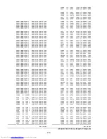
. . . V DC voltages measured in
PLAY MODE
with following conditions:
"+10V" = 10V
"+5V" = 5V
EVM
V
4.5V
7877
from
on
part1
10R
3809
470R
3809
2864
22p
2854
47n
3716
470R
3716
470R
DOBM
7877
from
on
part1
DOBM
10R
3712
1R
3717
10R
3712
to 1805
to 1805
COAX2
COAX2
COAX1
5802
920927152B
1
2
3
4
6
7
8
2865
22n
digital out circuitry - 75
Ω
version (not on all versions)
digital out circuitry
(not for 75
Ω
Versions)
Summary of Contents for FW-C399/25
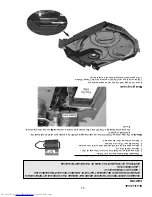
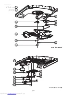
Page 6: ...10 4 Service Position ...


