


3-55
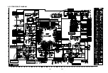
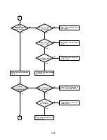
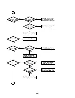
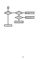
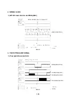
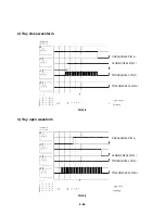
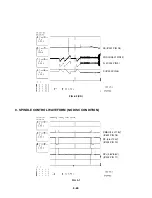
2. Test & debug flow
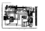
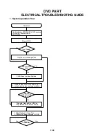
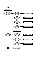
TEST
Check the POWER PART
No
Yes
No
Yes
No
No
No
Yes
Yes
Check the POWER PART
Check the regulators or diode(D601).
Check the cable connection.
(PDV02)
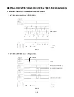
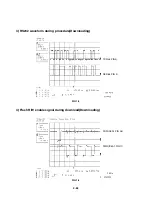
1. Check 27MHz system clock.
2. Check systemreset circuit.
3. Check FLASH R/Wenable signal PRD,
RWR.
4. Check RS232 SIGNALS.
5. Check FLASH Memory related circui t.
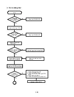
Check the
AC Vol tage
Power PCBA (110V
or 220V)
Switch on the Power PCBA
Is
the DC Vol tage
outputs OK?
(5V, 3.3V, 8V, 12V)
Is 3.3V and 2.5V DC
outputs normal on main
PCBA?
Update
FLASH(IC5A1)
successfully?
Replace FLASH( IC5A1)
A
Communication between
VCR & DVD is normally?
Connect to PC RS232 Cable and
update the FLASH memory code.
Make sure the main
PCBA don't
Summary of Contents for DVD755VR
Page 8: ...Directions for Use ...
Page 9: ......
Page 10: ......
Page 11: ......
Page 12: ......
Page 13: ......
Page 14: ......
Page 15: ......
Page 16: ......
Page 17: ......
Page 18: ......
Page 19: ......
Page 20: ......
Page 21: ......
Page 22: ......
Page 23: ......
Page 24: ......
Page 25: ......
Page 26: ...Personal Notes ...
Page 49: ......
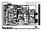
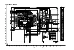
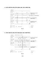
Page 56: ...3 32 3 33 2 TU IF NICAM A2 CIRCUIT DIAGRAM EE MODE VIDEO TU MODE AUDIO COMBI SCART ...
Page 59: ...3 38 3 39 5 SCART JACK CIRCUIT DIAGRAM OPTIONAL PART COMBI SCART ...
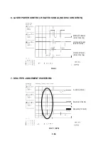
Page 61: ...3 42 3 43 7 TIMER CIRCUIT DIAGRAM ...
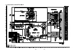
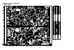
Page 65: ...3 50 3 51 PRINTED CIRCUIT DIAGRAMS 1 MAIN P C BOARD LOCATION GUIDE ...
Page 66: ...3 52 3 53 2 SMPS P C BOARD LOCATION GUIDE 3 TIMER P C BOARD LOCATION GUIDE 4 KEY P C BOARD ...
Page 67: ......
Page 93: ......
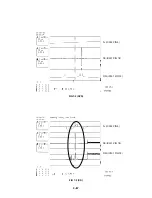
Page 96: ...3 83 3 84 3 AUDIO CIRCUIT DIAGRAM COMBI SCART MTK 03 3 25 SR17447A ...
Page 97: ...3 85 3 86 4 AV JACK CIRCUIT DIAGRAM COMBI SCART MTK 03 3 25 SR17446A ...
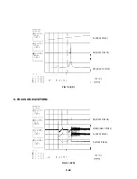
Page 100: ...3 91 3 92 PRINTED CIRCUIT DIAGRAMS 1 MAIN P C BOARD LOCATION GUIDE ...
Page 101: ......
Page 133: ...MEMO ...
Page 134: ...EXPLODED VIEW 1 Deck Mechanism Exploded View 5 1 CONTENTS SECTION 5 MECHANISM OF DVD PART ...


