4-9
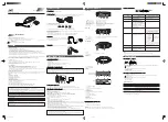
Remote reception is insensitive or fails.
No
Remote reception is
insensitive or fails.
Check if the remote
control works properly.
Check battery
Check R315
ǃ
C315
Use an oscilloscope to check
if there is output waveform
from the first pin IR of the
remote censor after pressing
button on the remote control.
REM301(PIN1 - RC waveform)
Check if there is IR
signal on pin 134 of U1
Check if the power
supply voltage to the
remote censor is normal
Go
No
No
No
Yes
Yes
Yes
Correct connection
Yes
Change U1
IR waveform
Trouble shooting chart
Summary of Contents for DivX DVP3146K
Page 27: ...6 6 6 6 Power Board Print Layout Bottom Side for DVP3126 K XX ...
Page 29: ...6 8 6 8 Power Board Print Layout Bottom Side for DVP3146 K XX DVP3148K XX ...
Page 34: ...6 13 6 13 Main Board Print Layout Top Side for DVP3126 K XX DVP3146 K XX DVP3148K XX ...
Page 35: ...6 14 6 14 Main Board Print Layout Bottom Side for DVP3126 K XX DVP3146 K XX DVP3148K XX ...
Page 40: ...6 19 6 19 Main Board Print Layout Top Side for DVP3146K 93 ...
Page 41: ...6 20 6 20 Main Board Print Layout Bottom Side for DVP3146K 93 ...