background image

3 - 2 

Loader repair Instruction for BDP3100/5100

/ 3080/98


Preliminaries (at O.E.M. supplier site) 

After scanning BARCODE on the new LOADER in supplier – TCL factory, print the 

one-dimensional code which generated by scanner and computer on label, then paste it into 

LOADER. If FA test passed , break off   the protection point under    the LOADER. 

Repair Procedure in workshop 

1. In region’s workshop, to install loader in the machine then weld the open protection point. 

Keep the set to connect the TV and power on, press keys “5””1””7””7” on Remote Control 

when in the HOME menu, then the menu will be displayed.   

2. Select “Enter Barcode Info” from the menu, input the BARCODE of the LOADER and wait 

until  the OSD displays “PASS”, press “STOP” key on Remote Control to go back to the 

menu.

3. Select “Laser check”, confirm whether the cable is connected and welded protection point is 

ok.

4. Restart the set, test CD, DVD, BD discs. If ok, the LOADER replacing procedure is finish. 

Summary of Contents for BDP3080/98

Page 1: ...s 1 2 Safety Instruction Warning Notes 1 3 Mechanical and Dismantling Instructions 2 Software Version Upgrades Region Code Change 3 Trouble Shooting Chart 4 Set Wiring Diagram 5 Electrical Diagrams and PCB layouts 6 Set Mechanical Exploded view Parts List 7 Revision List 8 BDP3080 98 BDP3100 12 05 51 96 55 93 98 X78 BDP5100 12 93 98 05 51 First Generation This service manual is for BDP3100 5100 Fi...

Page 2: ...hange 1 1 Technical Specifications For on line product support please use the following website http www p4c philips com cgi bin dcbint cpproduct_selector pl Here is product information available as well as getting started user manuals frequently asked questions and software drivers 1 2 Directions for Use You can download this information from the following websites http www philips com support ht...

Page 3: ...d voltages with and without aerial signal Measure the voltages in the power supply section both in normal operation and in stand by These values are indicated by means of the appropriate symbols 2 3 2 Schematic Notes All resistor values are in ohms and the value multiplier is often used to indicate the decimal point location e g 2K2 indicates 2 2 k Resistor values with no multiplier may be indicat...

Page 4: ... sources are expected to have a possible dangerous impact others of quite high potential are of limited current and are sometimes held in less regard Always respect voltages While some may not be dangerous in themselves they can cause unexpected reactions that are best avoided Before reaching into a powered TV set it is best to test the high voltage insulation It is easy to do and is a good servic...

Page 5: ...Frequency Interlaced Scan mode where two fields are used to form one frame Each field contains half the number of the total amount of lines The fields are written in pairs causing line flicker IR Infra Red IRQ Interrupt Request ITU 656 The ITU Radio communication Sector ITU R is a standards body subcommittee of the International Telecommunication Union relating to radio communication ITU 656 a k a...

Page 6: ...s SD Standard Definition SDA Serial Data I2 C SDA F DAta Signal on Fast I2C bus SDI Serial Digital Interface see ITU 656 SDRAM Synchronous DRAM SECAM SEequence Couleur Avec Mémoire Color system mainly used in France and East Europe Color carriers 4 406250 MHz and 4 250000 MHz SIF Sound Intermediate Frequency SMPS Switched Mode Power Supply SoC System on Chip SOG Sync On Green SOPS Self Oscillating...

Page 7: ...98 X 78 98 05 12 51 93 98 ASSY POWER BOARD M M M C M C M C M C M C M C M M M M C M C M ASSY MAIN BOARD M M M C M C M C M C M C M C M M M M C M C M ASSY SWITCH BOARD M M M M M M M M M M M M M M ASSY FRONT CONTROL BOARD M M M C M C M C M C M C M C M M M M C M C M BDP5100 Board in used TIPS C Component Lever Repair M Module Lever Repair X Used BDP3100 ...

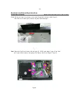
Page 8: ...the Top Cover Figure 1 Figure 1 Step2 If it is necessary to dismantle Loader or Front Panel the Front door should be removed first Figure 2 Note Make sure to operate gently otherwise the guider would be damaged Figure 2 2 1 Please kindly note that dismantle the front door assembly carefully to avoid damage tray and the front door Detailed information please refer to the model set ...

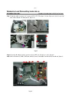
Page 9: ...ure 3 Note Make sure to operate gently otherwise the guider would be damaged Figure 3 Step4 Dismantling Front Panel disconnect the connectors J3 CN502 need release 3 snaps of Front Panel and 2 snaps of bottom cabinet then gently pull the Panel out from the set Figure 4 Figure 6 Figure 4 2 2 Detailed information please refer to the model set XP6 XP3 XP4 J3 XP2 ...

Page 10: ...n Board first disconnect the connector XP2 and then remove 6 screws Figure 6 Step7 Disconnect connector CN504 CN502 and remove 6 screws on Power Board to dismantle the Power Board Figure 6 Step5 Dismantling Loader disconnect the 3 connectors XP6 XP3 XP4 aiming in the below figure and remove 4 screws that connects the loader and the bottom cabinet Figure 4 5 ...

Page 11: ...herwise the Main board will be Cancel Start damaged entirely 4 Press Right cursor button to choose Start then press OK 5 The software will updagrde and screen will display as below Upgrade is ongoing Please wait Please do not unplug or switch off the device 6 The screen will display as below when upgrading complete Upgrade has completed successfully Power off after 5s Power Off 5 Restart the set B...

Page 12: ...gion s workshop to install loader in the machine then weld the open protection point Keep the set to connect the TV and power on press keys 5 1 7 7 on Remote Control when in the HOME menu then the menu will be displayed 2 Select Enter Barcode Info from the menu input the BARCODE of the LOADER and wait until the OSD displays PASS press STOP key on Remote Control to go back to the menu 3 Select Lase...

Page 13: ...in 8 9 6 arrive the condition JP2 3 4 5 Correct connection Replace U4 or VFD Yes Yes Yes No Check 28V 5V 12V voltage on the power and front board Check the front board signals SCK SDA STB 1 Check whether bad solder exists on U3 and pins of VFD 2 Check whether the circuit connected to K1 K2 K3 K4 K5 K6 is broken Fix the connection JP1 on front board and CN502 on power board Trouble shooting chart 4...

Page 14: ...V and U6 8 12V Check whether the audio signal is right from the U6 1 7 Check If the C511 C501 is on Add the two set Yes No Go Check whether the audio signal is right from the U915 9 10 11 12 No audio output Yes Trouble shooting chart 4 2 Replace the U915 Replace the U6 Yes NO NO ...

Page 15: ...rol does not work NO Replace the battery for remote controller Check whether the remote controller s battery is exhausted or not Check the IR1 power supply is OK IR1 3 is about 5V Check the VCC net no front board Replace IR1 Yes Trouble shooting chart 4 3 ...

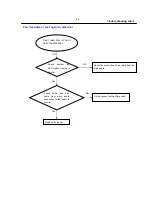
Page 16: ... from the main board Can t read disc or can t open the disk door Check 45pin and 8pin cable from main board connection to the loader is normal Replace the loader NO GO Check whether the DVD loader running is normal Fix the connection the 45pin cable NO Yes Trouble shooting chart 4 4 ...

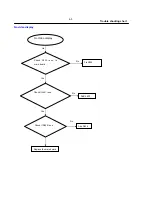
Page 17: ...No video display Check if L451 is on Go No No No Video display Yes Fix R302 Check R302 is on in main board Add L451 Replace the main board Yes Check If R454 is on No Add R454 Trouble shooting chart 4 5 ...

Page 18: ...824 VFD DRIVER S16312 IR FB TO MB 9IN FB TO MB 9PIN SWITCH BOARD STANDBY LED STANDBY LED DDR2 POWER G2992 COMPONENT L R CVBS COAX USB RS232 USB TAY IN OUT TRAY IN OUT BOARD OPU SANYOU 412 TRAVERSE 4PIN 4PIN 45PIN connect board 8PIN 8PIN FFC RS232 for FE 45PIN FFC OPU 7 1AV AV 220 IN IR GND VSTB VCLK VD GND PCON POWER 5VSTB PCON 24V GND 12V POWER LED 2 GND VCC_P VCC_P GND GND 12V_P 12V GND 5VSTB LO...

Page 19: ...47pF C12 47pF 47 USB003 XX2 USB P600 USB connector NC 47 USB003 XX2 USB P600 USB connector NC 1 2 3 4 5 6 R36 10K R36 10K R10 10K R10 10K U4 PT6312 U4 PT6312 SW1 1 SW2 2 SW3 3 SW4 4 SDout 5 SDin 6 GND 7 SCLK 8 CS 9 KEY1 10 KEY2 11 KEY3 12 KEY4 13 VDD 14 SEG1 K1 15 SEG2 K2 16 SEG3 K3 17 SEG4 K4 18 SEG5 K5 19 SEG6 K6 20 SEG7 21 SEG8 22 SEG9 23 SEG10 24 SEG11 25 SEG12 26 VEE 27 SEG13 28 SEG14 29 SEG1...

Page 20: ...A A B B C C D D E E 1 1 2 2 3 3 4 4 SWITCH BOARD C1 47Pf C1 47Pf D1 LED2_5 D1 LED2_5 K6 POWER K6 POWER CON1 PICH 2 0 CON1 PICH 2 0 3 2 1 Switch Board Circuit Diagram 6 2 6 2 ...

Page 21: ...0 1uF C508 0 1uF PAS PAS R536 22k R536 22k J2 0 ohm J2 0 ohm PAS PAS C503 100PF C503 100PF Q506 S8550 Q506 S8550 CE510 1000uF 16V CE510 1000uF 16V R501 2 2K R501 2 2K R507 1M 1206 1 R507 1M 1206 1 U503 TL431 U503 TL431 2 1 3 C505 0 47uF 63V C505 0 47uF 63V PAS PAS C509 0 1uF C509 0 1uF PAS PAS R524 2 2k R524 2 2k R508 1M 1206 1 R508 1M 1206 1 C511 0 1uF 50V C511 0 1uF 50V FB501 2 2uH FB501 2 2uH R...

Page 22: ...SS 23 TPIP 24 V3P3 25 AGND 26 nRST 27 EN_USB1 SCL 28 EN_USB2 SDA 29 USBFLG2 nINT 30 FB3 31 CMP3 32 EN_BCK3 33 PGND3B 34 PGND3A 35 PH3B 36 PH3A 37 VINB3B 38 VINB3A 39 BST3 40 USBOUT1 41 VINU 42 USBOUT2 43 USBFLG1 VCTRL 44 nBOR nHOT 45 VMON1 46 VMON2 47 12C_ADD 48 PGND 49 R118 1K 1 R118 1K 1 FB712 0R FB712 0R R74 10K R74 10K C45 1000pF C45 1000pF TP10 TP10 Q305 CES2302 Q305 CES2302 1 2 3 U4 UTC LD11...

Page 23: ... 0 1uF C105 0 1uF C130 4 7uF 0805 C C130 4 7uF 0805 C C110 0 1uF C110 0 1uF RN103 100X4R 0402 RP8 RN103 100X4R 0402 RP8 1 8 2 7 3 6 4 5 C104 0 1uF C104 0 1uF C149 0 1uF C149 0 1uF C114 0 1uF C114 0 1uF R106 100R 0603 R R106 100R 0603 R C154 NC 0805 C C154 NC 0805 C C147 0 1uF C147 0 1uF C135 0 1uF C135 0 1uF R107 NC 0603 R R107 NC 0603 R R101 0R R101 0R C116 0 1uF C116 0 1uF C142 0 1uF C142 0 1uF ...

Page 24: ... C236 0 1uF C236 0 1uF C239 0 1uF 0402 C C239 0 1uF 0402 C C203 0 1uF C203 0 1uF C225 0 1uF C225 0 1uF C227 0 1uF C227 0 1uF C202 0 1uF C202 0 1uF C220 0 1uF C220 0 1uF C230 0 1uF C230 0 1uF R204 100R R204 100R RN202 100X4R 0402 RP8 RN202 100X4R 0402 RP8 1 8 2 7 3 6 4 5 RN201 100X4R 0402 RP8 RN201 100X4R 0402 RP8 1 8 2 7 3 6 4 5 C228 0 1uF C228 0 1uF C212 0 1uF C212 0 1uF R203 0R R203 0R R200 0R R...

Page 25: ... C33 DACOUT3 B32 DACOUT4 A31 DACOUT5 C31 DACOUT6 D30 DACFS E33 AVDD12_HDMI G29 AVDD12_HDMI F30 AVDD33_HDMI H26 AVDD33_HDMI J27 AVSS12_HDMI H28 AVSS12_HDMI J29 AVSS33_HDMI G27 AVSS33_HDMI F28 CLK_M A29 CLK_P C29 CH0_M B28 CH0_P D28 CH1_M A27 CH1_P C27 CH2_M B26 CH2_P D26 HTPLG G39 CEC E43 HDMISD E41 HDMISCK F40 EXT_CAP B30 EXT_RES E29 NS_TSTP BA1 NS_TSTN AY2 NS_CKIN33 F6 NS_RFIP K8 NS_RFIN H4 SPBCK...

Page 26: ...40 TP440 FB351 0R FB351 0R R379 0R R379 0R FB356 0R FB356 0R R382 NC R382 NC TP420 TP420 TP55 TP55 TP359 TP359 TVS Arrays D350 RClamp0522P TVS Arrays D350 RClamp0522P 1 1 2 2 GND 3 GND 4 5 5 6 6 R1064 10K R1064 10K TP421 TP421 TP366 TP366 TP441 TP441 FB355 0R FB355 0R C361 0 1uF C361 0 1uF TP422 TP422 R1065 10K R1065 10K TP351 TP351 C157 0 1UF C157 0 1UF R376 10K R376 10K R353 NC R353 NC FB353 0R ...

Page 27: ... 10K R393 10K R53 4 7K R53 4 7K C385 NC C385 NC R401 4 7K R401 4 7K SKEY SKEY C351 100pF NC C351 100pF NC R411 10K NC R411 10K NC R409 2 2K NC R409 2 2K NC POWER POWER FB359 0R FB359 0R C366 100pF NC C366 100pF NC OPEN OPEN C389 0 1uF C389 0 1uF UATXD UATXD R397 4 7K R397 4 7K IR IR R429 10K R429 10K R398 10K R398 10K V_CLK V_CLK C352 5pF NC C352 5pF NC R405 10K R405 10K R423 4 7K R423 4 7K R414 1...

Page 28: ...F SDCLK_1 SDCLK_1 TP381 TP381 SD_P_CTL_1 SD_P_CTL_1 C402 0 1uF C402 0 1uF R426 0R R426 0R TP374 TP374 C396 0 1uF C396 0 1uF TP429 TP429 C398 0 1uF C398 0 1uF TP432 TP432 TP403 TP403 C417 10uF 6 3V C417 10uF 6 3V TP373 TP373 C401 0 1uF C401 0 1uF TP434 TP434 TP382 TP382 C409 0 1uF C409 0 1uF C399 0 1uF C399 0 1uF FB361 FB 0603 FB361 FB 0603 U100F MT8530_DDR2 U100F MT8530_DDR2 VCCK Y20 VCCK AB20 VCC...

Page 29: ...454 0R R454 0R C1008 33PF NC C1008 33PF NC L453 0 22uH L453 0 22uH R467 75_1 R R467 75_1 R R1403 0R R1403 0R R450 100R R450 100R C509 10pF NC C509 10pF NC R536 91_1 NC R536 91_1 NC C455 47pF C455 47pF C1002 0 1uF C1002 0 1uF C627 100PF C627 100PF D451 DIODE SMD BAV99 D451 DIODE SMD BAV99 1 3 2 C510 10pF NC C510 10pF NC D454 DIODE SMD BAV99 D454 DIODE SMD BAV99 1 3 2 R461 75_1 R R461 75_1 R C607 10...

Page 30: ...CSN 6 CDTI 8 CCLK 7 AOUTR 10 AOUTL 12 AOUTR 9 AOUTL 11 LRCK 4 CE18 100uF 16V CE18 100uF 16V D525 1N4148 D525 1N4148 5 1K 30K R77 1 5 1K 30K R77 1 2 1 470R 5 1K R86 1 470R 5 1K R86 1 2 1 D524 1N4148 D524 1N4148 R1361 10K R1361 10K 3300PF 1000PF C48 3300PF 1000PF C48 1 2 R512 470R R512 470R R507 3 3K R507 3 3K C61 0 1uF C61 0 1uF CE17 100uF 16V CE17 100uF 16V D526 1N4148 NC D526 1N4148 NC R135 NC 10...

Page 31: ...4 10R 0805 R R1294 10R 0805 R R20 10R R20 10R R712 0R R712 0R R738 330R R738 330R R752 10K R752 10K R717 0R R717 0R R1404 49 9R 0603 R R1404 49 9R 0603 R C708 10pF C708 10pF L860 TDK ACM2012H 900 2P 0 DLW21SN900SQ2L 2 L860 TDK ACM2012H 900 2P 0 DLW21SN900SQ2L 2 1 3 2 4 R741 0R R741 0R R743 10K R743 10K R708 33R R708 33R R751 10K NC R751 10K NC R1299 0R NC R1299 0R NC R709 0R R709 0R C704 0 1uF C70...

Page 32: ...E_GIO2 E3 FE_GIO11 D2 FE_GIO10 H8 FE_GIO9 E5 FE_GIO8 L9 FE_GIO7 G5 FE_GIO6 G9 FE_GIO5 J5 FE_GIO4 J7 FE_AVDD12_RX AP8 FE_SRXP AR1 FE_SRXN AR3 FE_STXN AP2 FE_STXP AN1 FE_STXVDD12 AP6 FE_SPLLVDD12 AN7 FE_SVDD33 AL7 FE_SXVDD33 AM6 FE_PLAY AH2 FE_LIMIT AG3 FE_DVDD12I V10 FE_GIO3 AG1 FE_EJECT AH4 FE_TRAYOUT AK4 FE_TRAYIN AJ5 FE_GIO1 AG9 FE_GIO0 AD8 FE_FSOURCE AH8 FE_XTAL25MI AJ3 FE_XTAL25MO AJ1 FE_EQBIA...

Page 33: ...F 42 LOIN 41 FOIN 40 TOIN 39 TLIN 38 TL 37 TL 36 FO 35 FO 34 GND 33 5VCC 32 TO 31 TO 30 GND 29 LO 28 LO 27 VM3 26 ACTRST 25 STTH 24 SPGS 23 VM1 22 R760 1K R760 1K F_R110 0R F_R110 0R F_C75 4 7uF F_C75 4 7uF GIO8 GIO8 W W F_C87 NC F_C87 NC R754 1K R754 1K A A F_R96 10K F_R96 10K XP3 8x1 W HOUSING XP3 8x1 W HOUSING 1 2 3 4 5 6 7 8 F_CE17 220uF 16V F_CE17 220uF 16V F_R111121R_1 F_R111121R_1 XP5 10x1 ...

Page 34: ...Front Board Print layout Top and Bottom side 6 16 6 16 ...

Page 35: ...Power Board Print layout Bottom side Switch Board Print layout Bottom side 6 17 6 17 ...

Page 36: ...Main Board Print layout Top side 6 18 6 18 ...

Page 37: ...Main Board Print layout Bottom side 6 19 6 19 ...

Page 38: ...loded view for BDP3100 12 05 51 55 93 96 98 X78 BDP3080 98 It is a general mechanical exploded view for BDP3100 BDP3080 98 pls refer to the model set for detailed information ASSY1 includes components 2 3 4 21 22 ...

Page 39: ...EXPLODED VIEW FOR BDP5100 12 93 98 05 7 2 EXPLODED VIEW FOR BDP5100 12 93 98 05 ASS Y 1 includes components 3 4 5 22 23 ...

Page 40: ... JC20 1 JP3 996510031263 FLAT WIRE 3P L200 PH 3Y SAN 3P 1 JP4 996510031269 USB CABLE 4PIN 2MM300MMPH JC20 1 PCORD 996510001537 POWER CORD 1 5M 1 RC 996510041223 REMOTE CONTROL 1 Screws List y t Q n o i t p i r c s e D o N C N 2 1 o N 7 7 F B 6 X 6 2 B W E R C S T S 9 6 W E R C S T S 11 16 2 3 F B 8 X 3 B W E R C S T S 12 2 B 6 X 3 W E R C S C M 15 9 F B 6 X 3 B W E R C S T S 18 4 F B 7 X 3 B W E R...

Page 41: ...40MM FH JC20 1 JP3 996510031263 FLAT WIRE 3P L200 PH 3Y SAN 3P 1 JP4 996510031269 USB CABLE 4PIN 2MM300MMPH JC20 1 PCORD 996510026331 POWER CORD 1 RC 996510041223 REMOTE CONTROL 1 Screws List No 12NC No Description Q ty 7 ˉ S T SCREW B 2 6 X 6 BF 7 9 ˉ S T SCREW 6 11 16 ˉ S T SCREW B 3 X 8 BF 3 2 12 ˉ M C SCREW 3 X 6 B 15 ˉ S T SCREW B3 X 6 BF 9 18 ˉ S T SCREW B 3 X 7 BF 4 SAFETY PRECAUTION The pa...

Page 42: ... JC20 1 JP3 996510031263 FLAT WIRE 3P L200 PH 3Y SAN 3P 1 JP4 996510031377 USB CABLE 4PIN L200MM 1 PCORD 996510001537 POWER CORD 1 RC 996510041223 REMOTE CONTROL 1 XP3 996510031379 8PIN WIRE PH1 0MM L100MM B 1 Screws List No 12NC No Description Q ty 7 ˉ S T SCREW B 2 6 X 6 BF 7 9 ˉ S T SCREW 6 11 16 ˉ S T SCREW B 3 X 8 BF 3 2 12 ˉ M C SCREW 3 X 6 B 2 15 ˉ S T SCREW B3 X 6 BF 9 18 ˉ S T SCREW B 3 X...

Page 43: ... JP3 996510031263 FLAT WIRE 3P L200 PH 3Y SAN 3P 1 JP4 996510031377 USB CABLE 4PIN L200MM 1 PCORD 996510001537 POWER CORD 1 RC 996510041223 REMOTE CONTROL 1 XP3 996510031379 8PIN WIRE PH1 0MM L100MM B 1 Screws List No 12NC No Description Q ty 7 ˉ S T SCREW B 2 6 X 6 BF 7 9 ˉ S T SCREW 6 11 16 ˉ S T SCREW B 3 X 8 BF 3 2 12 ˉ M C SCREW 3 X 6 B 1 15 ˉ S T SCREW B3 X 6 BF 9 18 ˉ S T SCREW B 3 X 7 BF 4...

Page 44: ...MB DDR2 SDRAM 1 ZD501 996510007898 DIODE ZENER 24V 1 2W 5 1 U102 996510032917 64X16MB DDR2 SDRAM 1 ZD502 996500015716 DIODE ZENER 33V 1 2W 5 1 U103 996510032912 REGULATOR G2992B 1 ZD503 996510007898 DIODE ZENER 24V 1 2W 5 1 U2 996510032951 IC AZ1117 LDO 3 3V 1 2V 1 ZD504 996510032942 DIODE ZENER BZX79 C11 11V À5 U201 996510032918 IC NY512M DDR2 1066MHZ 1 U202 996510032918 IC NY512M DDR2 1066MHZ 1 ...

Page 45: ...1 2W 5 1 U103 996510032912 REGULATOR G2992B 1 ZD503 996510007898 DIODE ZENER 24V 1 2W 5 1 U2 996510032951 IC AZ1117 LDO 3 3V 1 2V 1 ZD504 996510032942 DIODE ZENER BZX79 C11 11V À5 U201 996510032918 IC NY512M DDR2 1066MHZ 1 U202 996510032918 IC NY512M DDR2 1066MHZ 1 U351 996510032916 2GB NAND FLASH 1 No 12NC No Description Q ty U352 996510032943 IC TPS652 PWR MANAGEMENT 1 13 996510032952 BACK PLATE...

Page 46: ...96510032917 64X16MB DDR2 SDRAM 1 ZD501 996510007898 DIODE ZENER 24V 1 2W 5 1 U102 996510032917 64X16MB DDR2 SDRAM 1 ZD502 996500015716 DIODE ZENER 33V 1 2W 5 1 U103 996510032912 REGULATOR G2992B 1 ZD503 996510007898 DIODE ZENER 24V 1 2W 5 1 U2 996510032951 IC AZ1117 LDO 3 3V 1 2V 1 ZD504 996510032942 DIODE ZENER BZX79 C11 11V À5 U201 996510032918 IC NY512M DDR2 1066MHZ 1 U202 996510032918 IC NY512...

Page 47: ...M 1 ZD501 996510007898 DIODE ZENER 24V 1 2W 5 1 U102 996510032917 64X16MB DDR2 SDRAM 1 ZD502 996500015716 DIODE ZENER 33V 1 2W 5 1 U103 996510032912 REGULATOR G2992B 1 ZD503 996510007898 DIODE ZENER 24V 1 2W 5 1 U2 996510032951 IC AZ1117 LDO 3 3V 1 2V 1 ZD504 996510032942 DIODE ZENER BZX79 C11 11V À5 U201 996510032918 IC NY512M DDR2 1066MHZ 1 U202 996510032918 IC NY512M DDR2 1066MHZ 1 U351 9965100...

Page 48: ...DR2 SDRAM 1 ZD502 996500015716 DIODE ZENER 33V 1 2W 5 1 U102 996510032917 64X16MB DDR2 SDRAM 1 ZD503 996510007898 DIODE ZENER 24V 1 2W 5 1 U103 996510032912 REGULATOR G2992B 1 ZD504 996510032942 DIODE ZENER BZX79 C11 11V À5 U2 996510032951 IC AZ1117 LDO 3 3V 1 2V 1 U201 996510032918 IC NY512M DDR2 1066MHZ 1 U202 996510032918 IC NY512M DDR2 1066MHZ 1 No 12NC No Description Q ty U351 996510034432 IC...

Page 49: ... G2992B 1 ZD504 996510032942 DIODE ZENER BZX79 C11 11V À5 U2 996510032951 IC AZ1117 LDO 3 3V 1 2V 1 U201 996510032918 IC NY512M DDR2 1066MHZ 1 U202 996510032918 IC NY512M DDR2 1066MHZ 1 No 12NC No Description Q ty U351 996510034429 IC 2GB NAND FLASH BDP5100 93 1 14 996510034428 BACK PLATE 1 U352 996510032943 IC TPS652 PWR MANAGEMENT 1 18 996510031557 TOP COVER 1 U4 996510031778 IC 3 3V 1 9 9965100...

Page 50: ...15716 DIODE ZENER 33V 1 2W 5 1 U101 996510032917 64X16MB DDR2 SDRAM 1 ZD503 996510007898 DIODE ZENER 24V 1 2W 5 1 U102 996510032917 64X16MB DDR2 SDRAM 1 ZD504 996510032942 DIODE ZENER BZX79 C11 11V À5 U103 996510032912 REGULATOR G2992B 1 U2 996510032951 IC AZ1117 LDO 3 3V 1 2V 1 U201 996510032918 IC NY512M DDR2 1066MHZ 1 No 12NC No Description Q ty U202 996510032918 IC NY512M DDR2 1066MHZ 1 14 996...

Page 51: ...DE ZENER 24V 1 2W 5 1 U101 996510032917 64X16MB DDR2 SDRAM 1 ZD502 996500015716 DIODE ZENER 33V 1 2W 5 1 U102 996510032917 64X16MB DDR2 SDRAM 1 ZD503 996510007898 DIODE ZENER 24V 1 2W 5 1 U103 996510032912 REGULATOR G2992B 1 ZD504 996510032942 DIODE ZENER BZX79 C11 11V À5 1 U2 996510032951 IC AZ1117 LDO 3 3V 1 2V 1 U201 996510032918 IC NY512M DDR2 1066MHZ 1 U202 996510032918 IC NY512M DDR2 1066MHZ...

Page 52: ...2 996500015716 DIODE ZENER 33V 1 2W 5 1 U101 996510032917 64X16MB DDR2 SDRAM 1 ZD503 996510007898 DIODE ZENER 24V 1 2W 5 1 U102 996510032917 64X16MB DDR2 SDRAM 1 ZD504 996510032942 DIODE ZENER BZX79 C11 11V À5 1 U103 996510032912 REGULATOR G2992B 1 U2 996510032951 IC AZ1117 LDO 3 3V 1 2V 1 U201 996510032918 IC NY512M DDR2 1066MHZ 1 No 12NC No Description Q ty U202 996510032918 IC NY512M DDR2 1066M...

Page 53: ...H JC20 1 JP3 996510031263 FLAT WIRE 3P L200 PH 3Y SAN 3P 1 JP4 996510032946 4PIN CABLE L200MM 1 AC 996510036469 EU DETACHABLE POWER CORD 1 5M 1 RC 996510041223 REMOTE CONTROL 1 XP3 996510031379 8PIN WIRE PH1 0MM L100MM B 1 Screws List y t Q n o i t p i r c s e D o N C N 2 1 o N 7 7 F B 6 X 6 2 B W E R C S T S 9 6 W E R C S T S 11 16 2 3 F B 8 X 3 B W E R C S T S 12 1 B 6 X 3 W E R C S C M 15 9 F B...

Page 54: ...3100 05 BDP3100 51 Version 1 1 BDP5100 12 added Version 1 2 Added BDP3100 55 3100 93 3100 98 3100X 78 Version 1 3 Added BDP3080 98 Version 1 4 Added BDP5100 05 51 Version 1 5 Page 7 3 Partslist updated Change 14 996510031443 MAIN BOARD ASS Y WAS 996510031262 8 1 ...

Reviews: