background image

Service Modes, Error Codes, and Fault Finding

EN 23

TPM6.1E LA

5.

2011-Jun-10

back to 

div. table

Note: If the USB flash drive is not detected after power up, 
disconnect it and re-insert it.

4.

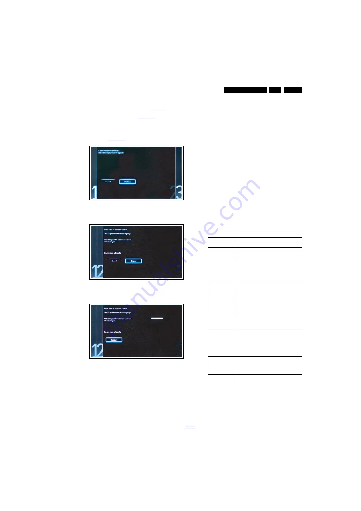
Select [Update] and press OK. See 

Figure 5-9

.

5.

To proceed, In next menu select [Start] and press OK to 
start software updates. Se

Figure 5-10

.

6.

Upgrading will now begins and the status of the updating 
progress will be displayed. 

7.

When the TV software is updated. Remove your USB flash 
drive, then select [Restart] and press OK to restart the 
TV.See 

Figure 5-11

.

Figure 5-9 Update the TV software [1/3]

Figure 5-10 Update the TV software [2/3]

Figure 5-11 Update the TV software [3/3]

Note:

Do not remove the USB flash drive during the software 
update.

If a power failure occurs during the update, do not remove 
the USB flash drive from the TV. The TV will continue the 
software update as soon as the power comes up again.

If an error occurs during the update retry the procedure or 
contact the dealer.

We do not recommend downgrading to an older version.

Once the upgrade is finished, use the PC to remove the TV 
software from the USB portable memory.

5.5.6

Content and Usage of the One-Zip Software File

Below you find a content explanation of the One-Zip file, and 
instructions on how and when to use it. Only files that are 
relevant for Service are mentioned here. 

EDID_clustername.zip: Contains the EDID content of the 
different EDID NVMs. See ComPair for further instructions.

FUS_clustername_version.zip: Contains the 
“autorun.upg” which is needed to upgrade the TV main 
software and the software download application.

NVM_clustername_version.zip: Default NVM content. 
Must be programmed via ComPair.

5.5.7

How to Copy NVM Data to/from USB

When copying data to and from a USB memory stick, the folder 
“repair” is used. When inserting an empty USB memory stick, 
and downloading data to the stick, the TV will create this folder. 
When sending data from a USB memory stick to a TV, the 
intended data must be available in the “repair” folder.
Note that when copying EDID data to the TV, all necessary 
EDID files must be in this folder.
Service mode overview for your reference. Please adapt 
accordingly: 

Table 5-2 Service mode overview

19080_207_110324.eps 

110324 

19080_208_110324.eps 

110324 

19080_209_110324.eps 

110324 

Service Modes

Description

SAM

Service alignment mode

SDM

Service default Mode

CSM

3-page compact CSM pages. There will be 
CSM dump to USB-stick upon entering 
CSM-mode

USB SW 
upgradeable

SW-upgrading of flash memories 
MTK-chips MT5366 can be done via USB. 
The main SW can be upgraded via 
Autorun.upg

NVM-Editor in 
SAM

NVM-editor will function as in the past: 
Address and Value field is a decimal value 
via digit entry

Service Data

New Service data in SAM for CTN, Prod. 
no., 12NC programming with virtual key 
board

USB copy/paste 
in SAM

Channel list, NVM data, Readable info, 
EDID

UART logging

There will be printout available in UART. No 
specifications of the printout, per MTK 
provision/definition.

Vcom flicker 
alignment

“147852” + “OK” (for flickering adjustment).
TV to be put to external source other than 
TV, then adjust with arrow up/down and 
Left right, the Vcom value in the display will 
change with the arrow key, one adjusted, 
press OK and then press menu to exit

Tcon NVM 
default & 
Programmer 
default loading

“42662” + “OK”

Blind SAM

RC sequence “062598” + “Menu” + 
“Panel code”

Clear Buffer

RC sequence “062599” + “OK” or via SAM

Summary of Contents for 42PFL3606H/12

Page 1: ...3 Adapter A01 63 65 66 Inverter A02 64 65 66 A01 715G4738 PSU Berlinale 67 Adapter A01 67 69 70 LED A02 68 69 70 B 715G4609 SSB Thriller 71 System Power 1 B01 71 87 88 System Power 2 B02 72 87 88 Peripheral B03 73 87 88 Connector USB RS232 B04 74 87 88 Audio IO Headphone B05 75 87 88 Speaker B06 76 87 88 Video IO SPDIF B07 77 87 88 SCART B08 78 87 88 VGA Input B09 79 87 88 LVDS B10 80 87 88 DRAM I...

Page 2: ...d questions and software drivers Table 2 1 Described Model Numbers Note The given Model Numbers are subject to change 2 2 Directions for Use Directions for use can be downloaded from the following websites http www philips com support http www p4c philips com Model Number Styling Published in 32PFL3606H 12 Thriller 3122 785 19080 32PFL3606H 58 Thriller 3122 785 19080 32PFL3606H 60 Thriller 3122 78...

Page 3: ...ical Specs Diversity and Connections EN 3 TPM6 1E LA 2 2011 Jun 10 back to div table 2 3 Connections Figure 2 1 Connection overview Thriller styling 9 11 7 8 10 13 14 1 2 4 5 6 12 19080_001_110301 eps 110331 ...

Page 4: ...it k 3 UART_RX Receive j 4 USB2 0 Figure 2 3 USB type A 1 5V k 2 Data jk 3 Data jk 4 Ground Gnd H 5 Head phone Output Bk Head phone 80 600 Ω 10 mW ot 6 HDMI Digital Video Digital Audio In Figure 2 4 HDMI type A connector 1 D2 Data channel j 2 Shield Gnd H 3 D2 Data channel j 4 D1 Data channel j 5 Shield Gnd H 6 D1 Data channel j 7 D0 Data channel j 8 Shield Gnd H 9 D0 Data channel j 10 CLK Data ch...

Page 5: ...ed Gnd H 12 DDC_SDA DDC data j 13 H sync 0 5 V j 14 V sync 0 5 V j 15 DDC_SCL DDC clock j 11 Audio In Left Right VGA Gn Audio L R in 0 5 VRMS 10 kΩ jq 12 EXT1 Video RGB YC In CVBS In Out Audio In Out Figure 2 7 SCART connector 1 Audio R 0 5 VRMS 1 kΩ k 2 Audio R 0 5 VRMS 10 kΩ j 3 Audio L 0 5 VRMS 1 kΩ k 4 Ground Audio Gnd H 5 Ground Blue Gnd H 6 Audio L 0 5 VRMS 10 kΩ j 7 Video Blue C out 0 7 VPP...

Page 6: ...rrier at 475 25 MHz for PAL or 61 25 MHz for NTSC channel 3 Where necessary measure the waveforms and voltages with D and without E aerial signal Measure the voltages in the power supply section both in normal operation G and in stand by F These values are indicated by means of the appropriate symbols 3 3 2 Schematic Notes All resistor values are in ohms and the value multiplier is often used to i...

Page 7: ...re sometimes held in less regard Always respect voltages While some may not be dangerous in themselves they can cause unexpected reactions that are best avoided Before reaching into a powered TV set it is best to test the high voltage insulation It is easy to do and is a good service precaution 3 4 Abbreviation List 0 6 12 SCART switch control signal on A V board 0 loop through AUX to TV 6 play 16...

Page 8: ... the International Telecommunication Union relating to radio communication ITU 656 a k a SDI is a digitized video format used for broadcast grade video Uncompressed digital component or digital composite signals can be used The SDI signal is self synchronizing uses 8 bit or 10 bit data words and has a maximum data rate of 270 Mbit s with a minimum bandwidth of 135 MHz iTV Institutional TeleVision ...

Page 9: ...erial Clock I2C SCL F CLock Signal on Fast I2 C bus SD Standard Definition SDA Serial Data I2C SDA F DAta Signal on Fast I2 C bus SDI Serial Digital Interface see ITU 656 SDRAM Synchronous DRAM SECAM SEequence Couleur Avec Mémoire Colour system mainly used in France and East Europe Colour carriers 4 406250 MHz and 4 250000 MHz SIF Sound Intermediate Frequency SMPS Switched Mode Power Supply SoC Sy...

Page 10: ...ressing 4 2 Service Positions 4 3 Assembly Panel Removal Thriller styling 4 4 Assembly Panel Removal Berlinale styling 4 5 Set Re assembly Notes Figures below can deviate slightly from the actual situation due to the different set executions 4 1 Cable Dressing Figure 4 1 Cable dressing 32 Thriller styling 19080_100_110302 eps 110302 ...

Page 11: ... Instructions EN 11 TPM6 1E LA 4 2011 Jun 10 back to div table Figure 4 2 Cable dressing 42 Thriller styling Figure 4 3 Cable dressing 32 Berlinale styling 19080_101_110302 eps 110302 19080_110_110404 eps 110404 ...

Page 12: ... Lift the rear cover from the TV Make sure that wires and flat foils are not damaged while lifting the rear cover from the set Figure 4 4 Rear cover removal 4 3 2 Small Signal Board SSB Refer to Figure 4 5 and Figure 4 6 for details Caution it is mandatory to remount all different screws at their original position during re assembly Failure to do so may result in damaging the SSB 1 Release the cli...

Page 13: ...ase the clips that hold the board and take it out from the bezel 7 Unplug both the connectors from the IR LED board When defective replace the whole unit Figure 4 7 IR LED removal 4 3 7 Keyboard Control unit 1 Remove the speakers as described earlier 2 Remove the stand as described earlier 3 Release the clamps that hold board cable 4 Remove the fixation screws 1 2 that secure the LCD panel with th...

Page 14: ...n be careful as these are very fragile connectors Take the flat foils out of their connectors 2 Unplug all other connectors 3 Remove all fixation screws from the SSB Note that one screw is located below the upper flat foil cable 4 Take out the SSB together with side and bottom I O bracket 5 Remove the screws between the bottom Y Pb and L R audio connectors 6 Remove the side and bottom I O bracket ...

Page 15: ...se tapes from the speaker cables 5 Take the left and right speakers out When defective replace the both units 4 4 8 IR LED Keyboard Refer to Figure 4 11 for details 1 Remove the stand bracket as described earlier 2 Release the connectors 1 from the IR LED Keyboard 3 Caution The board is fitted to the bezel by double sided tape 4 Use the slot type screw driver to detach the IR LED Keyboard from the...

Page 16: ... the flat foils out of their connectors 9 Remove the fixation screws 2 at the top sides and bottom of the panel that secure the LED panel with the bezel Remove all metal clips from their position Be careful not to break the clicks that secure by metal brackets to keep those in position 10 Lift the LED Panel from the bezel When defective replace the whole unit Figure 4 13 LED panel removal 4 5 Set ...

Page 17: ...Note For the new model range a new remote control RC is used with some renamed buttons This has an impact on the activation of the Service modes For instance the old MENU button is now called HOME or is indicated by a house icon 5 2 1 General Next items are applicable to all Service Modes or are general Life Timer During the life time cycle of the TV set a timer is kept called Op Hour It counts th...

Page 18: ...t the option bytes Ten codes in two rows are possible Figure 5 2 SDM menu How to Navigate As this mode is read only there is not much to navigate To switch to other modes use one of the following methods Command MENU from the user remote will enter the normal user menu brightness contrast color etc with SDM OSD remaining and pressing MENU key again will return to the last status of SDM again To pr...

Page 19: ...s the life timer The timer counts normal operation hours but does not count Stand by hours Main SW ID e g TPM61E 1 071C See paragraph Software Identification Version and Cluster for the SW name definition ERR e g 000 000 000 000 000 Shows all errors detected since the last time the buffer was erased Five errors possible OP1 e g 012 004 192 002 184 032 007 030 Used to read out the option bytes See ...

Page 20: ...ced or is initialized after corruption this production code has to be re written to NVM 1 3 Installation date Indicates the date of the first installation of the TV This date is acquired via time extraction 1 4 Option Code 1 Gives the option codes of option group 1 as set in SAM 1 5 Option Code 2 Gives the option codes of option group 2 as set in SAM 1 6 SSB Gives an identification of the SSB as s...

Page 21: ...ital background tasks completed Swith On previously in Standby Semi Standby Mains Power Plug Standby Soft Mode Command Received Power tact switch Switch Off Mains Power Plug Switch Off Mains Power Plug Swith On previously in Standby Soft Mode Mains Power Plug Standby commands Received RC Standby key Standby Soft Mode Command Received previously in Standby Soft Mode Power tact switch TV Wakeup comm...

Page 22: ...ct your local support desk 5 5 Software Upgrading 5 5 1 Description It is possible for the user to upgrade the main software via the USB port This allows replacement of a software image in a stand alone set A description on how to upgrade the main software can be found in the DFU or on the Philips website 5 5 2 Introduction Philips continuously tries to improve its products and it s recommend that...

Page 23: ...n NVM_clustername_version zip Default NVM content Must be programmed via ComPair 5 5 7 How to Copy NVM Data to from USB When copying data to and from a USB memory stick the folder repair is used When inserting an empty USB memory stick and downloading data to the stick the TV will create this folder When sending data from a USB memory stick to a TV the intended data must be available in the repair...

Page 24: ...0 hours the error buffer resets automatically Note If you exit SAM by disconnecting the mains from the television set the error buffer is not reset 5 7 The Blinking LED Procedure 5 7 1 Introduction The software is capable of identifying different kinds of errors Because it is possible that more than one error can occur over time an error buffer is available which is capable of storing the last fiv...

Page 25: ...ed to insure that the cooling is guaranteed otherwise the Class D IC could break down in short time 5 8 8 CSM When CSM is activated and there is a USB memory stick connected to the TV the software will dump the complete CSM content to the USB memory stick The file Csm txt will be saved in the root of the USB memory stick 5 8 9 Loudspeakers Make sure that the volume is set to minimum during disconn...

Page 26: ... on the RC then press STORE to store the aligned values to the NVM Restore the initial picture settings after the alignments Table 6 1 White tone default settings This group setting of colour temperature will be applied automatically to the TV VGA HDMI and AV sources 6 4 Option Settings 6 4 1 Introduction The microprocessor communicates with a large number of I2 C ICs in the set To ensure good com...

Page 27: ...use the NVM editor and Dealer options items in SAM do not forget to store After a repaired SSB has been mounted in the set repair on board level the type number CTN and production code of the TV has to be set according to the type plate of the set For this you can use the NVM editor in SAM The loading of the CTN and production code can also be done via ComPair Model number programming In case of a...

Page 28: ...GAMMA TPS65192RHDR Level shifter for 3000 Thriller series MAX17119ETI Level shifter for 5000 Berlinale series 7 1 2 TPM6 1E Architecture Overview For details about the chassis block diagrams refer to chapter 9 Block Diagrams An overview of the TPM6 1E architecture can be found in Figure 7 1 Figure 7 2 and Figure 7 3 Figure 7 1 Architecture of Thriller 19080_210_110324 eps 110405 6 6 3 5 T M 1 1 M ...

Page 29: ...o c T r e t t i m s n a r T S D V L ni i m n i d l i u b D T A s s e l w a S D I D E 2 0 C 4 2 D I D E 2 0 C 4 2 t f i h S l e v e L 9 1 1 7 1 M I X A M D I D E 2 0 C 4 2 D I D E 2 0 C 4 2 C 2 I o i d u A C 2 I m e t s y S 3 I M D H C R A 1 I M D H r o s n e s t h g i L 19080_212_110324 eps 110401 I V C f o L R o i d u A P M A o i d u A R T W B 9 3 3 A T S F I D M V N 8 2 1 C 4 2 s r e k a e p S t...

Page 30: ...1 Jun 10 back to div table 7 1 3 SSB Cell Layout Thriller Figure 7 4 Thriller SSB layout cells top view 19080_213_110324 eps 110401 AUDIO CLASS D DC DC TUNER SERVICE CONNECTOR TCON MT5366 DDR2 HDMI SWITCH COMMON INTERFACE DIGITAL I O ANALOG I O ...

Page 31: ...ack to div table 7 1 4 SSB Cell Layout Berlinale Figure 7 5 Berlinale SSB layout cells top view 19080_232_110407 eps 110407 AUDIO CLASS D DC DC TUNER SERVICE CONNECTOR MT5366 DDR2 HDMI SWITCH COMMON INTERFACE DIGITAL I O DIGITAL I O ANALOG I O ANALOG I O ...

Page 32: ...issues The output voltages to the chassis are 5V 3V3 STANDBY Stand by mode only 12V on mode 24V for audio circuit Figure 7 6 Thriller power board management Figure 7 7 Berlinale xxPFL56xx xx power board management Bridge Diode PFC Control Inverter Control Inverter Transformer EMI FILTER AC Inlet PWM Control Power Transformer Standby Power Standby Transformer Lamp R Lamp L 24V Audio power 12V Panel...

Page 33: ...t a l u g e R A 5 3 0 0 5 U 1 5 2 S D M T 1 o t 3 W S I M D H 2 0 0 7 U 3 4 T 7 1 1 1 G r o t a l u g e R A 1 5 0 0 1 U 5 3 1 5 T M o m e D C T 3 0 0 4 2 0 0 4 U 2 R D D 4 0 0 4 U F U 3 4 T 7 1 1 1 G r o t a l u g e R A 5 h s a l F 5 0 0 4 U 3 V 3 D D V D 3 3V SSB B S R W P O K C C V K C C V W S _ V 5 e v r e s e R 6 0 0 7 U F U 3 4 T 3 3 7 1 1 1 G r o t a l u g e R A 1 R W P _ C A D A 2 V 1 D D V...

Page 34: ...001 pins 5 and 6 24V input from the power supply for audio in active mode connector CN7001 pins 7 STB_PWR3V3 3V3SB 24V 12V U4001 MT5366 U7004 G5795 GMT 3A Buck U6004 TPA6132 HP AMP U7005 G1084 GMT 5A Regulator U5003 TMDS351 U7002 G1117 T43 1A Regulator U1005 MT5135 T C Demo U4002 U4003 DDR2 U4004 G1117 1A Regulator U4005 NAND Flash DVDD3V3 STB_PWR3V3 PWR_ON VCCK VCCK 5V_SW U7006 Reserve G1117 33T4...

Page 35: ... eps 110325 DIGITAL ANALOG POWER DVDD3V3 AVDD3V3 form 5V_SW RA RB Vout DVDD3V3 5V_SW AVDD3V3 R7020 130R 1 R7020 130R 1 C7027 100uF 16V C7027 100uF 16V C7022 100uF 16V C7022 100uF 16V FB7005 220R 2000mA FB7005 220R 2000mA 1 2 C7028 100N 16V C7028 100N 16V FB7006 220R 2000mA FB7006 220R 2000mA 1 2 C7023 10uF 10V C7023 10uF 10V C7029 100N 16V C7029 100N 16V R7013 0R05 4A 1 4W R7013 0R05 4A 1 4W R7021...

Page 36: ... CN4005 1 2 3 4 5 6 7 iTV ǂǂ RC6 3V3SB 3V3SB D4002 BAV99 D4002 BAV99 3 1 2 CN4006 CONN CN4006 CONN 1 2 3 4 5 R4073 NC 0 OHM 5 1 16W R4073 NC 0 OHM 5 1 16W R4071 NC 0 OHM 5 1 16W R4071 NC 0 OHM 5 1 16W R4072 100OHM1 16W R4072 100OHM1 16W 19080_222_110325 eps 110401 U0TX U0RX ǂǂ ǂǂ U0RX U0TX 3V3SB 3V3SB 5VSB R4080 4 7K1 16W R4080 4 7K1 16W CN4001 NC CONN CN4001 NC CONN 1 2 3 4 R4081 100 OHM 1 10W R4...

Page 37: ...3 65 PAD_D6 66 PAD_D14 67 PAD_D7 68 PAD_D15 69 PAD_CE1_ 70 DVDD33 71 DGND33 72 PAD_A10 73 PAD_VS1_ 74 PAD_OE_ 75 PAD_IORD_ 76 PAD_A11 77 PAD_IOWR_ 78 PAD_A9 79 PAD_A17 80 PAD_A8 81 DGND10 82 DVDD10 83 PAD_A18 84 PAD_A13 85 PAD_A19 86 PAD_A14 87 PAD_A20 88 DVDD33 89 DGND33 90 PAD_WE_ 91 PAD_A21 92 PAD_READY 93 PAD_A22 94 PAD_A16 95 PAD_A23 96 PAD_A15 97 PAD_A24 98 PAD_A12 99 PAD_A25 100 PAD_A7 101 ...

Page 38: ... Thermal Pad 29 C7114 1uF Z 10V C7114 1uF Z 10V R7104 0R05OHM1 16W R7104 0R05OHM1 16W C7111 10uF 16V C7111 10uF 16V R7122 NC 10OHM1 16W R7122 NC 10OHM1 16W R7116 NC 10OHM1 16W R7116 NC 10OHM1 16W R7120 10OHM1 16W R7120 10OHM1 16W D7012 NC B540C D7012 NC B540C 1 2 R7118 20R 5 1 16W R7118 20R 5 1 16W R7117 20R 5 1 16W R7117 20R 5 1 16W R7103 0R05OHM1 16W R7103 0R05OHM1 16W C7112 100N 16V C7112 100N ...

Page 39: ...ws the internal block diagrams and pin configurations of ICs that are drawn as black boxes in the electrical diagrams with the exception of memory and logic ICs 8 1 Diagram Peripheral B03 MT5366CVGG BGA 479 IC U4001 Figure 8 1 Internal block diagram 19080_300_110316 eps 110330 Block diagram VADC 4 ...

Page 40: ...LA 8 2011 Jun 10 back to div table Figure 8 2 Pin configuration 1 2 19080_301_110316 eps 110316 Pinning information 479 1 2 3 4 5 6 7 8 9 10 11 12 A B C D E F G H J K L M N P R T U V W Y AA AB AC AD AE LB 1 2 3 4 5 6 7 8 9 10 11 12 ...

Page 41: ...n 10 back to div table Figure 8 3 Pin configuration 2 2 19080_302_110316 eps 110316 Pinning information 13 14 15 16 17 18 19 20 21 22 23 24 25 RT A B C D E F G H J K L M N P R T U V W Y AA AB AC AD AE 13 14 15 16 17 18 19 20 21 22 23 24 25 RB ...

Page 42: ... 7 8 9 10 11 12 13 14 15 16 17 18 19 20 21 22 23 24 25 26 27 28 29 30 31 32 3 2 A 6 1 A 2 2 A Y D A E R 1 2 A E W _ S S V D 3 3 D D V D 0 2 A 4 1 A 9 1 A 3 1 A 8 1 A 0 1 D D V D S S V D 8 A 7 1 A 9 A R W O I _ 1 1 A D R O I _ E O _ 1 S V _ 0 1 A S S V D 3 3 D D V D 1 E C _ 5 1 D 7 D 4 1 D 6 D 3 1 D I P S _ E L C I P S _ A T A D I P S _ L C K R V P _ S T _ 1 A T A D R V P _ S T _ 0 A T A D S _ S T ...

Page 43: ...NK SDA_SINK HPD_SINK S1 S2 Control Logic Y4 Z4 VSADJ TMDS Driver TMDS Driver TMDS Driver TMDS Driver EQ VDD Vcc TMDS Rx Vcc TMDS Rx Vcc TMDS Rx Vcc TMDS Rx Vcc TMDS Rx Vcc TMDS Rx Vcc TMDS Rx Vcc TMDS Rx A14 B14 A13 B13 A12 B12 A11 B11 A24 B24 A23 B23 A22 B22 A21 B21 HPD1 HPD2 SCL1 SDA1 SCL2 SDA2 Y3 Z3 Y1 Z1 Y2 Z2 HPD DDC 2 to 1 MUX RINT RINT RINT RINT RINT RINT RINT RINT RINT RINT RINT RINT RINT ...

Page 44: ...NC NC Vcc NC NC GND NC NC Vcc NC NC GND VSADJ 17 18 19 20 21 22 23 24 25 26 27 28 29 30 31 32 4 Y Vcc GND Vcc GND SCL_SINK SDA_SINK HPD_SINK S1 48 47 46 45 44 43 42 41 40 39 38 37 36 35 34 33 A14 B14 Vcc A13 B13 GND A12 B12 Vcc A11 B11 SCL1 SDA1 HPD1 EQ S2 64 63 62 61 60 59 58 57 56 55 54 53 52 51 50 49 C N 4 2 A Vcc GND Vcc SCL2 SDA2 HPD2 VDD Z4 3 Y Z3 2 Y Z2 1 Y Z1 4 2 B 3 2 A 3 2 B 2 2 A 2 2 B ...

Page 45: ...0809 Block diagram Pinning information 1 HPVDD CPP INL INL INR INR PGND CPN 2 3 4 12 11 10 9 16 15 14 13 5 6 7 8 R T U O G0 G1 S S V P H L T U O D N G S D D V N E Click and Pop Suppression HPVDD HPVSS HPVDD HPVSS Charge Pump INR INR INL INL OUTL OUTR CPP CPN HPVSS G0 EN Thermal Protection Gain Select G1 VDD Supply Control PGND SGND HPVDD Resistor Array 1 F 1 F 2 2 F Short Circuit Protection Resist...

Page 46: ...36 35 34 33 32 31 30 29 28 27 26 25 24 23 22 21 20 19 VDD_DIG GND_DIG SCL SDA INT_LINE RESET SDI LRCKI BICKI XTI GND_PLL FILTER_PLL VDD_PLL PWRDN GND_DIG VDD_DIG TWARN OUT4A EAPD OUT4B GND_SUB SA TEST_MODE VSS VCC_REG OUT2B GND2 VCC2 OUT2A OUT1B VCC1 GND1 OUT1A GND_REG VDD CONFIG OUT3B FFX3B OUT3A FFX3A Protection current thermal Logic Regulators Bias Power control FFX PLL Volume control Channel 1...

Page 47: ...4 13 GND 12 11 10 9 8 7 6 5 16 GND VIN N I V PH PH 1 2 3 4 SS TR PowerPAD 17 QFN16 RTE PACKAGE TOP VIEW ERROR AMPLIFIER Boot Charge Boot UVLO UVLO Current Sense Oscillator with PLL Frequency Shift Slope Compensation PWM Comparator Minimum COMP Clamp Maximum Clamp Voltage Reference Overload Recovery VSENSE SS TR COMP RT CLK PH BOOT VIN AGND Thermal Shutdown EN Enable Comparator Shutdown Logic Shutd...

Page 48: ... FB2 DEL1 REF GND2 EN1 3 25 37 COMP FBN 38 39 40 PGOOD CRST AGND AGND DRVN CTL LX1 32 15 LX2 LX1 31 16 17 18 19 20 LX2 DLP FBP CPGND OUT 8 9 10 21 PGND STEP DOWN OSC VL LX2 GND2 OUT FB2 VIN REF AGND DEL1 VL VL VIN VIN 12V 3 3V 2A 150mV STEP UP POWER UP SEQUENCE HV SWITCH BLOCK NEGATIVE REG POSITIVE REG IN2 LX1 PGND FB1 COMP FSEL AGND SWI SWO PGOOD PGOOD 3 3V VL BST VGOFF 6V 100mA REF VL AVDD 16V 1...

Page 49: ...ERS I2C REGISTERS I2C INTERFACE MTP MEMORY 10 BIT DAC 10 GMA1 AVDD 10 10 BIT DAC 10 GMA2 10 10 BIT DAC 10 GMA3 10 10 BIT DAC 10 GMA4 10 10 BIT DAC 10 GMA5 10 10 BIT DAC 10 GMA6 10 10 BIT DAC 10 GMA7 10 10 BIT DAC 10 GMA8 10 DVDD SDA SCL A0 10 BIT DAC 10 AVDD_AMP VCOM_FB GND_AMP VCOM 10 GND 19 20 18 17 7 6 8 A0 AGND_AMP VCOM 9 SDA GMA5 GMA3 GMA2 GMA6 1 2 GMA7 4 5 15 14 12 11 GMA8 SCL N C AVDD AVDD_...

Page 50: ...am Pinning information RE OUT1 OUT2 OUT3 OUT4 OUT5 OUT6 OUT7 IN1 IN2 IN3 IN4 IN5 IN6 IN7 IN8 IN9 OUT8 OUT9 VGL VGH2 VGH1 FLK3 DISCHARGE VSENSE GND VREF FLK2 FLK1 IN7 1 IN6 2 IN5 3 IN4 4 5 IN9 6 IN8 2 N I 8 1 N I 9 10 1 1 12 1 T U O 13 28 1 K L F 27 L G V 26 D N G 25 E R 24 1 H G V 23 OUT9 21 OUT8 20 OUT7 19 OUT6 18 OUT5 17 OUT4 16 Exposed IN3 7 OUT3 15 2 T U O 14 2 H G V 22 E G R A H C S I D 3 K L...

Page 51: ... IC U7109 Figure 8 13 Internal block diagram and pin configuration 19080_308_110317 eps 110317 Pinning information RE A3 A9 13 12 11 10 9 8 28 27 26 25 24 23 22 1 3 4 2 6 5 7 15 14 A4 A7 A8 VSENSE FLK2 A5 A6 FLK1 Y4 Y5 Y6 Y8 Y7 Y3 GON1 FLK3 A1 YDCHG Y9 MAXIM PF61 21 20 19 18 17 16 GOFF GON2 Y1 Y2 GND A2 Block diagram ...

Page 52: ... Vcc A11 B11 SCL1 SDA1 HPD1 EQ S2 64 63 62 61 60 59 58 57 56 55 54 53 52 51 50 49 HPD3 A24 B24 Vcc A23 B23 GND A22 B22 Vcc A21 B21 SCL2 SDA2 HPD2 VDD SCL_SINK SDA_SINK HPD_SINK S1 S2 Control Logic Y4 Z4 VSADJ TMDS Driver TMDS Driver TMDS Driver TMDS Driver EQ VDD Vcc RINT TMDS Rx RINT Vcc RINT TMDS Rx RINT Vcc RINT TMDS Rx RINT Vcc RINT TMDS Rx RINT Vcc RINT TMDS Rx RINT Vcc RINT TMDS Rx RINT Vcc ...

Page 53: ...53 B MAIN POWER SUPPLY 1054 CN902 1 ENA 2 DIM 3 12V 4 12V 5 GND 6 GND 7 GND 8 24V 9 24V 10 S B 11 5V 12 5V 13 14 INV_OK TO BACKLIGHT CN6004 1 RSPK 2 RSPK 3 LSPK 4 LSPK CN803 1 HV2 2 HV2 3 HV2 DANGEROUS HIGH VOLTAGE CN802 1 HV2 2 HV2 3 HV2 DANGEROUS HIGH VOLTAGE LCD DISPLAY A 84003 8001 CN4003 9 KEY2 8 KEY1 7 GND 6 DV33SB 5 DV33SB 4 GND 3 RC6 2 LED_G 1 LED_R CN7001 13 LED_ON 12 STB_PWR5V 11 STB_PWR...

Page 54: ... CN001 4P CN301 9P CN903 1 ENA 2 DIM 3 12V 4 12V 5 GND 6 GND 7 GND 8 24V 9 24V 10 S B 11 5V 12 5V 13 14 GND TO BACKLIGHT CN6004 1 RSPK 2 RSPK 3 LSPK 4 LSPK CN803 1 HV2 2 HV2 3 HV2 DANGEROUS HIGH VOLTAGE CN802 1 HV2 2 HV2 3 HV2 DANGEROUS HIGH VOLTAGE LCD DISPLAY A J 8001 CN4003 9 KEY2 8 KEY1 7 GND 6 DV33SB 5 DV33SB 4 GND 3 RC6 2 LED_G 1 LED_R CN7001 13 LED_ON 12 STB_PWR5V 11 STB_PWR5V 10 STANDBY 9 ...

Page 55: ...LED7 8 LED6 7 LED5 6 LED4 5 LED3 4 LED2 3 LED1 2 1 LED RIGHT SPEAKER LEFT SPEAKER A CN7102 1 GMA1 2 GMA3 3 GMA4 4 GMA5 55 CK4 56 CK3 57 CK2 58 CK1 59 60 Z OUT CN7103 1 Z OUT 2 3 CK1 4 CK2 55 GMA9 56 GMA7 57 GMA5 58 GMA4 59 GMA3 60 GMA1 CN4003 1 LIGHT_SENSOR 2 GND 3 RC6 4 Green_Button 5 3V3SB 6 LED_G 7 Key1 8 5V_SW CN7001 1 STB_PWR3V3 2 STANDBY 3 GND 4 GND 5 12V 6 12V 7 24V 8 GND 9 INVERTER_ON_OFF ...

Page 56: ... u A C 2 I m e t s y S d a p y e K l a c o L 1 r P b P Y 1 S B V C e d i S F R r e n u T 2 I M D H I V D C P f o L R o i d u A e r P o i d u A p m A 0 8 5 4 M J N t u o R L 1 T R A C S 1 B S U 1 T R A C S l l u F h s a l F D N A N 128 MB z H G 3 3 1 3 R D D 128 MB 2 A G V C P S T t o l s d r a c I C M A C S D V L i n i M C D C D l i t u M 7 5 F P m o c V a m m a G 8 6 6 9 X A M V 2 1 p m A e n o h...

Page 57: ... 6 1 5 6 S P T m o c V a m m a G 0 3 6 8 0 F U B V 2 1 p m A e n o h p d a e H 2 3 1 6 A P T e n o h p d a e H S 2 I I M D H H C T I W S 1 5 3 S D M T C T V B D Demodulator r e l l o r t n o c I C 5 3 1 5 T M C 2 I r e n u T I C I C s t u p n i o i d u A g o l a n A s t u p n i o e d i V g o l a n A l e d o m C T B V D I P S z H 0 5 l e n a P n o c T o w d r a o b e t a G e c r u o S 6 6 3 5 T M 1...

Page 58: ...2 x B M 8 2 1 A G V C P S T t o l s d r a c I C M A C S D V L p m A e n o h p d a e H 2 3 1 6 A P T e n o h p d a e H S 2 I I M D H H C T I W S 1 5 3 S D M T C T V B D Demodulator r e l l o r t n o c I C 5 3 1 5 T M C 2 I r e n u T I C I C s t u p n i o i d u A g o l a n A s t u p n i o e d i V g o l a n A l e d o m C T B V D I P S 6 6 3 5 T M 1 1 M R A U C M o i d u a o e d i v G E P M r e d o c ...

Page 59: ...p 2 Mult 3 CS 4 Vcc 8 Driver 7 GND 6 ZCD 5 C954 470pF 250V_NC C954 ZD911 P6KE200A ZD911 P6KE200A 1 2 3 T902 PPH7019AL 3 T902 PPH7019AL 2 1 4 5 7 8 10 9 R909 1K 1 4W 5 R909 1K 1 4W 5 C912 47uF 50V C912 47uF 50V D906 RGP10D D906 RGP10D C943 330N 25V C943 330N 25V C928 470PF 1KV C928 470PF 1KV C911 2n2 500V C911 2n2 500V 1 2 D916 1N4148_NC D916 1N4148_NC ZD907 MTZJT 7213B ZD907 MTZJT 7213B 1 2 FB901 ...

Page 60: ...1 10K 1 8W 1 R815 3K6 1 8W 1 R815 3K6 1 8W 1 IC804 EL817MA IC804 EL817MA 1 2 4 3 CN803 CONN CN803 CONN 1 2 3 4 5 R803 68K 1 8W 1 _NC R803 68K 1 8W 1 _NC R822 10K 1 8W 1 R822 10K 1 8W 1 Q808 KIA431A AT P Q808 KIA431A AT P C804 2U2 25V C804 2U2 25V C817 56P 50V C817 56P 50V Q811 RK7002FD5T116 Q811 RK7002FD5T116 Q809 KIA431A AT P Q809 KIA431A AT P C810 470P 50V C810 470P 50V C834 10N 50V C834 10N 50V...

Page 61: ... Q808 J924 J923 J922 J910 J909 J915 C933 C952 M1 H2 H1 M2 M10 M7 M13 M5 FPAD4 M3 Q901 Q801 Q802 RV901 C902 C904 L905 T901 C809 C807 SG901 SG902 SG904 L904 L903 T902 D912 BD901 C901 FB903 L902 FB905 FB901 IC901 IC803 IC804 IC805 IC806 C802 C927 L901 C930 FB902 IC903 IC905 C938 C947 FB904 Q904 CN902 C909 HQ904 CN901 C912 FB906 CN802 CN803 T801 T803 L906 D916 C803 IC906 C903 C950 SG903 ZD903 ZD905 ZD...

Page 62: ... R816 R822 R823 R825 R826 R907 R924 R919 R831 R803 R805 R834 R835 R836 R911 R945 R837 R838 R812 R813 R923 R968 R969 R970 R957 R958 R959 R960 R961 R962 R963 R948 C917 C939 C940 C919 C931 C915 C913 C941 C935 C806 C812 C827 C808 C810 C914 C801 C813 C805 C811 C814 C821 C923 C916 C936 C922 C918 C815 C816 C819 C823 C825 C826 C828 C817 C832 C833 C834 C942 C943 C944 C945 C948 Q909 Q903 Q806 Q902 Q905 C830...

Page 63: ...2 47R 1 4W 5 C911 1UF450V C911 1UF450V F901 F901 3 4 1 2 Q905 BC857C Q905 BC857C D901 STTH5L06FP D901 STTH5L06FP R943 100 OHM 1 4W_NC R943 100 OHM 1 4W_NC C937 47UF 50V C937 47UF 50V C961 100N 50V C961 100N 50V R917 47OHM 5 1 8W R917 47OHM 5 1 8W FB902 BEAD FB902 BEAD 1 2 R912 5K1 5 1 8W R912 5K1 5 1 8W R976 1M 1 8W 5 R976 1M 1 8W 5 ZD903 MTZJ T 72 ZD903 MTZJ T 72 1 2 C931 270PF C931 270PF SG905 G...

Page 64: ...1 8W R829 0 OHM 5 1 8W IC805 EL817MA IC805 EL817MA 1 2 4 3 C833 2U2 25V C833 2U2 25V JR902 0R05 1 4W JR902 0R05 1 4W C820 1N 50V C820 1N 50V C824 10N 50V C824 10N 50V R819 390K 1 6W 5 R819 390K 1 6W 5 C802 0 33UF 500V C802 0 33UF 500V C801 100N 50V C801 100N 50V R837 20K 1 8W 1 R837 20K 1 8W 1 R824 10K 1 6W 5 R824 10K 1 6W 5 IC804 EL817MA IC804 EL817MA 1 2 4 3 R828 1K 1 4W 5 R828 1K 1 4W 5 IC808 K...

Page 65: ...945 R838 R923 R962 D917 D913 D902 C919 C931 C936 C922 C945 J901 J920 J919 J917 J929 J927 D910 C926 J906 J905 J921 IC907 IC904 C934 Q903 Q902 J931 R839 J924 J923 J922 R819 J909 J915 C933 M1 M2 M10 M7 M5 M3 SL20 SL19 SL3 SL9 SL10 SL11 SL12 SL18 SL1 SL2 T801 T904 T901 T802 T803 CN901 HD917 HD921 HQ903 CN802 CN803 F901 BD901 C927 C928 C921 C924 C803 C807 C809 C903 C901 C902 C904 C905 C910 C802 C911 TH...

Page 66: ...R912 R954 R955 R918 R964 R936 R801 R914 R941 R806 R802 R921 R908 R935 R938 R949 R922 R939 R917 R950 R820 R808 R811 R827 R821 R807 R942 R944 R937 R804 R913 R810 R814 R815 R816 R822 R823 R825 R826 R907 R831 R805 R834 R836 R911 R837 R812 R813 R970 R957 R958 R959 R961 R963 R948 C917 C939 C940 C915 C913 C935 C806 C812 C827 C808 C810 C914 C801 C813 C805 C811 C814 C821 C923 C916 C918 C815 C816 C819 C823 ...

Page 67: ...004DG IC9901 CAP004DG NC 1 D1 2 D1 3 NC 4 NC 5 D2 6 D2 7 NC 8 C9141 1U 25V C9141 1U 25V C9140 1U 25V C9140 1U 25V C9136 100P 50V C9136 100P 50V R9147 1MOHM 1 1 4W R9147 1MOHM 1 1 4W R9350 4R7 1 4W 5 R9350 4R7 1 4W 5 R9165 1K5 1 1 8W R9165 1K5 1 1 8W C9144 100N 50V C9144 100N 50V t TH9902 SCK101R55LSY t TH9902 SCK101R55LSY 1 2 ZD9303 BZX79 C9V1 ZD9303 BZX79 C9V1 1 2 R9164 2K 1 8W 5 R9164 2K 1 8W 5 ...

Page 68: ...34 1N 50V C8134 1N 50V C8107 10N 50V NC C8107 10N 50V NC R8120 1K OHM 5 1 8W R8120 1K OHM 5 1 8W R8166 100KOHM 5 1 8W R8166 100KOHM 5 1 8W C8114 10N 50V NC C8114 10N 50V NC C8103 10N 50V NC C8103 10N 50V NC D8102 1N4148W D8102 1N4148W R8146 1K OHM 5 1 8W C8125 2U2 16V C8125 2U2 16V Q8123 PZT2907A Q8123 PZT2907A R8119 10K OHM 5 1 8W R8119 10K OHM 5 1 8W R8167 100KOHM 5 1 8W R8167 100KOHM 5 1 8W R81...

Page 69: ...J9006 J9004 J9009 C9305 C9307 J9038 J9041 J9044 D8100 J9047 J9024 C9934 H1 H2 SL1 SL2 SL3 SL4 SL5 SL6 SL7 SL8 SL9 SL10 C9124 C9125 C9932 C9922 C9924 C9933 FB9130 FB9901 FB9902 R9900 RV9901 ZD9130 Q9121 Q9122 HD9121 C8104 C9114 FB8100 L9901 L9902 D9121 C9133 C9332 C9145 F9901 ZD9303 D9113 D9112 IC9301 C9118 T9111 C9803 C9804 C9123 C8105 C8106 C9112 C9113 C9121 C9122 BD9910 C9142 HD9112 R8161 R8113 ...

Page 70: ...1 C8121 C8122 C8124 C8126 C9102 C9324 C9325 C9326 C9327 R8120 R8129 R8144 R8145 R8146 R8147 R8148 R8149 R8150 R8151 R8152 R8153 R8157 R9316 R9326 R9337 R9339 R9342 R9343 R9344 R9345 R9340 R9341 Q9318 R8164 R8165 R8166 R8167 C8127 C8128 C8129 C8130 C8131 C8132 C8133 C8134 R8127 R8131 R9902 R8107 R8108 R9350 JR9005 R8160 R8114 R9143 R9338 R8102 C9308 R9168 R8134 R8135 R8136 R8137 R8138 R8139 R8140 R...

Page 71: ...R7024 NC 10K 1 10W R7007 NC 1K1 16W R7007 NC 1K1 16W Q7002 SI5441DC Q7002 SI5441DC D 1 D 2 D 3 G 4 S 5 D 6 D 7 D 8 R7010 10KOHM 5 1 8W R7010 10KOHM 5 1 8W C7006 NC 10U 10V C7006 NC 10U 10V C7021 22uF 10V C7021 22uF 10V C7028 100N 16V C7028 100N 16V FB7006 220R 2000mA FB7006 220R 2000mA 1 2 Q7003 BC847C Q7003 BC847C R7003 120R 1 1 10W R7003 120R 1 1 10W R7018 300R 1 16W 1 R7018 300R 1 16W 1 C7012 1...

Page 72: ...GND 2 4 5 6 7 8 9 10 11 12 13 14 15 16 17 R7031 0R051 8W R7031 0R051 8W C7038 100uF 16V C7038 100uF 16V R7032 NC 0R051 8W R7032 NC 0R051 8W C7036 NC 100UF 16V C7036 NC 100UF 16V R7037 5 1K 1 10W R7037 5 1K 1 10W R7038 10K1 16W R7038 10K1 16W C7037 NC 100uF 16V C7037 NC 100uF 16V R7035 10K 1 10W R7035 10K 1 10W C7039 1UF16V C7039 1UF16V C7040 4U7 10V C7040 4U7 10V Q7005 BC847C Q7005 BC847C U7006 NC...

Page 73: ...B15 AVSS12_PLL AA17 OPWRSB AB9 ORESET_ Y8 OIRI AC8 DVSS H6 DVSS M9 DVSS W19 DVSS Y19 DVSS W20 DVSS Y20 DVSS N9 DVSS L12 DVSS L13 DVSS L14 DVSS P9 DVSS R10 DVSS M11 DVSS M12 DVSS M13 DVSS M14 DVSS M15 DVSS M16 DVSS N11 DVSS N12 DVSS N13 DVSS N14 DVSS N15 DVSS N16 DVSS P11 DVSS P12 DVSS P13 DVSS P14 DVSS P15 DVSS P16 DVSS R11 DVSS R12 DVSS R13 DVSS R14 DVSS K12 DVSS K13 DVSS M10 DVSS N10 DVSS P10 U0...

Page 74: ...B4003 220R 2000mA FB4003 220R 2000mA 1 2 CN4001 NC CONN CN4001 NC CONN 1 2 3 4 1 2 3 4 CN4007 CONN 1 2 3 4 CN4007 CONN 1 2 3 4 6 5 R4208 4K7 1 16W 5 R4208 4K7 1 16W 5 R4065 100R 1 10W 5 R4065 100R 1 10W 5 R4069 100 OHM 1 10W R4069 100 OHM 1 10W R4068 0R05 1 10W R4068 0R05 1 10W U4009 NC G5250M1T1U U4009 NC G5250M1T1U OUT 1 GND 2 OC 3 EN 4 IN 5 R4081 100 OHM 1 10W R4081 100 OHM 1 10W R4118 0R05 1 1...

Page 75: ...6002 TP TP6002 TP C6023 1UF16V C6023 1UF16V TP6005 TP TP6005 TP FB6003 120R 3000mA FB6003 120R 3000mA 1 2 R6031 1 2K 1 16W 1 R6031 1 2K 1 16W 1 C6010 33P 50V C6010 33P 50V C6033 100N 50V C6033 100N 50V U6003 NJM4580M TE1 U6003 NJM4580M TE1 1OUT 1 1IN 2 1IN 3 VCC 4 2IN 5 2IN 6 2OUT 7 VCC 8 R6036 NC 1 2K 1 16W 1 R6036 NC 1 2K 1 16W 1 Q6002 BC847C Q6002 BC847C R6003 47R 1 10W 5 R6003 47R 1 10W 5 R603...

Page 76: ...FB6006 220R 2000mA 1 2 C6056 100N 50V C6056 100N 50V R6081 NC 4K7 1 10W 5 R6081 NC 4K7 1 10W 5 C6085 220UF 16V C6085 220UF 16V C6042 NC 330UF 35V C6042 NC 330UF 35V L6003 47UH L6003 47UH R6064 0R05 1 16W R6064 0R05 1 16W C6061 100N 16V C6061 100N 16V C6058 1N 50V C6058 1N 50V CN6004 CONN CN6004 CONN 1 2 3 4 FB6005 120R 600mA FB6005 120R 600mA 1 2 R6082 22K 1 16W 5 R6082 22K 1 16W 5 Q6001 BC857BW Q...

Page 77: ...NC 10N 50V R1050 30KOHM 1 16W 5 R1050 30KOHM 1 16W 5 C1199 33P 50V C1199 33P 50V C1029 10N 50V C1029 10N 50V C1014 10N 50V C1014 10N 50V C1005 100N 16V C1005 100N 16V R1013 100OHM1 16W R1013 100OHM1 16W R1051 30KOHM 1 16W 5 R1051 30KOHM 1 16W 5 C1191 NC 10N 50V C1191 NC 10N 50V C1009 10U 10V C1009 10U 10V ZD1006 NC UDZSNP5 6B ZD1006 NC UDZSNP5 6B 1 2 R1042 100 OHM 1 10W R1042 100 OHM 1 10W FB1004 ...

Page 78: ...0V R1077 30KOHM 1 16W 5 R1077 30KOHM 1 16W 5 R1059 47K1 16W R1059 47K1 16W C1046 NC 47pF 50V C1046 NC 47pF 50V R1082 0R05 1 16W R1082 0R05 1 16W R1063 100OHM1 16W R1063 100OHM1 16W C1073 10U 10V C1073 10U 10V D1024NC BAS316 D1024NC BAS316 A 1 K 2 FB1005 80 OHM FB1005 80 OHM 1 2 C1055 15PF50V C1055 15PF50V C1047 47pF 50V C1047 47pF 50V C1193 NC 10N 50V C1193 NC 10N 50V R1056 0R05 1 16W R1056 0R05 1...

Page 79: ...064 10NF 50V C1066 10U 10V C1066 10U 10V C1063 5pF 50V C1063 5pF 50V R1208 0R05OHM1 16W R1208 0R05OHM1 16W R1100 10K 1 10W R1100 10K 1 10W C1059 10NF 50V C1059 10NF 50V ZD1026 NC UDZSNP5 6B ZD1026 NC UDZSNP5 6B 1 2 R1104 100OHM1 16W R1104 100OHM1 16W ZD1157 NC VPORT0603100KV05 ZD1157 NC VPORT0603100KV05 1 2 R1084 0R05OHM1 16W R1084 0R05OHM1 16W Q1012 NC 2N7002 Q1012 NC 2N7002 ZD1023 NC UDZSNP5 6B ...

Page 80: ...PWR_EN0 5 13 LVDS_CTRL 15 BL_DIMMING 13 BL_ON OFF 13 USB_DM0 5 USB_DP0 5 BRIGHT_ADJ 2 INVERTER_ON_OFF 2 GND 2 3 4 5 6 7 8 9 10 12 13 14 15 16 17 RMLV0_P 17 LMLV0_N 17 LMLV0_P 17 RMLV3_P 17 RMLV2_P 17 RMLV1_P 17 RMLVCLK_N 17 RMLVCLK_P 17 LMLV5_P 17 LMLV4_P 17 LMLV3_P 17 LMLV2_P 17 LMLV1_P 17 RMLV3_N 17 RMLV2_N 17 RMLV1_N 17 RMLV5_N 17 RMLV4_N 17 LMLVCLK_P 17 LMLV5_N 17 LMLV4_N 17 LMLV3_N 17 LMLV2_N...

Page 81: ... B10 RDQ11 RDQ9 B15 RDQ10 RDQ10 A10 RDQ12 RDQ11 A15 RDQ15 RDQ12 C11 RDQ9 RDQ13 C15 RDQ8 RDQ14 C10 RDQ14 RDQ15 C14 RDQ22 RDQ16 G5 RDQ23 RDQ17 J5 RDQ17 RDQ18 H5 RDQ16 RDQ19 J4 RDQ20 RDQ20 H4 RDQ21 RDQ21 K4 RDQ19 RDQ22 G4 RDQ18 RDQ23 K3 RDQ26 RDQ24 J1 RDQ27 RDQ25 D2 RDQ29 RDQ26 J2 RDQ28 RDQ27 C1 RDQ31 RDQ28 H3 RDQ25 RDQ29 D1 RDQ24 RDQ30 J3 RDQ30 RDQ31 E2 RDQS0 RDQS0 B13 RDQS0_ RDQS0_ A13 RDQS1 RDQS1 ...

Page 82: ...D_TSCLK 15 DEMOD_TSVAL 15 DEMOD_TSSYNC 15 DEMOD_TSDATA0 15 SPI_DATA 15 SPI_CLE 15 CI_INT 15 DEMOD_RST 15 KEY_MENU_L_R_SOURCE 5 KEY_UP_DN_DCSW 5 LED_G 5 LED_R 5 LCD_Clock_SCL 5 LCD_Clock_SDA 5 STAND_BY 2 PWR5V_1 14 EDID_WEN 10 14 I2SAMP_RESET 7 POL_A 17 SOE_A 17 GVDD_ODD 17 GVDD_EVEN 17 GVST 17 GCLK1 17 GCLK2 17 GCLK3 17 GCLK4 17 GCLK5 17 GCLK6 17 FLK 17 DPM 17 TCON_PGOOD 17 LIGHT_SENSOR_IN 5 PWR5V...

Page 83: ... 1 16W 1 R5056 100R 1 16W 1 C5013 100N 16V C5013 100N 16V Q5006 NC BC847C Q5006 NC BC847C 3 2 1 D5006 BAS316 D5006 BAS316 A 1 K 2 Q5003 BC847C Q5003 BC847C 3 2 1 R5035 47K 1 10W R5035 47K 1 10W U5003 TMDS251PAGR U5003 TMDS251PAGR NC 1 NC 2 GND 3 NC 4 NC 5 Vcc 6 NC 7 NC 8 GND 9 NC 10 NC 11 Vcc 12 NC 13 NC 14 GND 15 VSADJ 16 TX2 17 TX2 18 Vcc 19 TX1 20 TX1 21 GND 22 TX0 23 TX0 24 Vcc 25 TXC 26 TXC 2...

Page 84: ...00N 16V R1154 1K 1 R1154 1K 1 R1156 NC 0R05 1 10W R1156 NC 0R05 1 10W R1119 22R 1 16W 5 R1119 22R 1 16W 5 R1125 NC 10K 1 R1125 NC 10K 1 R1141 51R 1 R1141 51R 1 R1131 22R 1 16W 5 R1131 22R 1 16W 5 C1089 NC 10uF 16V C1089 NC 10uF 16V R1114 22R 1 16W 5 R1114 22R 1 16W 5 FB1021 120R 600mA FB1021 120R 600mA 1 2 R1140 22R 1 16W 5 R1140 22R 1 16W 5 R1130 0R05 1 16W R1130 0R05 1 16W FB1015 220R 2000mA FB1...

Page 85: ...V C1169 NC 220pF 50V C1169 NC 220pF 50V C1162 NC 47nF 16V C1162 NC 47nF 16V C1157 220P 50V C1157 220P 50V R1201 75R 1 R1201 75R 1 R1197 0R05 1 16W R1197 0R05 1 16W C1168 220pF 50V C1168 220pF 50V R1184 NC 10K1 16W R1184 NC 10K1 16W R1183 100R 1 10W 5 R1183 100R 1 10W 5 C1170 10N 50V C1170 10N 50V R1185 NC 10K1 16W R1185 NC 10K1 16W R1203 0R05 1 16W R1203 0R05 1 16W TU1003 ENV57U09D5F B active ANT ...

Page 86: ... 50 49 48 47 46 45 44 43 42 41 40 39 38 37 36 35 34 33 32 31 61 62 D7012 NC B540C D7012 NC B540C 1 2 C7087 10uF 16V C7087 10uF 16V R7057 15K 1 R7057 15K 1 C7067 NC 27P50V C7067 NC 27P50V R7096 20R 5 1 16W R7096 20R 5 1 16W C7056 100N 25V C7056 100N 25V D7008 NC BAV99 D7008 NC BAV99 3 1 2 D7010 BAV99 D7010 BAV99 3 1 2 C7102 10uF 25V C7102 10uF 25V R7118 20R 5 1 16W R7118 20R 5 1 16W R7058 47K1 16W ...

Page 87: ...1008 FB1015 FB6004 FB6006 FB7001 FB7005 R1001 R1011 R1012 R1013 R1014 R1015 R1016 R1018 R1019 R1021 R1022 R1023 R1028 R1029 R1034 R1037 R1038 R1040 R1050 R1051 R1054 R1055 R1056 R1059 R1060 R1061 R1063 R1065 R1070 R1071 R1074 R1075 R1076 R1078 R1079 R1080 R1081 R1082 R1083 R1084 R1085 R1086 R1087 R1088 R1089 R1090 R1091 R1092 R1094 R1095 R1097 R1098 R1103 R1104 R1148 R1149 R1154 R1155 R1185 R1187 ...

Page 88: ...R3V3 INVERTER_ON_OFF BRIGHT_ADJ STANDBY PWR_ON OPWRSB STANDBY PWR_ON STB_PWR3V3 3V3SB 12V AVDD3V3 VCCK 12V 5V_SW 12V 5V_SW 3V3SB 24V 12V 3V3SB 12V U7004 G5795F11U U7004 G5795F11U BS 1 IN 2 LX 3 GND 4 FB 5 COMP 6 EN 7 SS 8 GND 9 C7006 NC 10U 10V C7006 NC 10U 10V R7014 0R05 4A 1 4W R7014 0R05 4A 1 4W R7047 22K 1 16W 5 R7047 22K 1 16W 5 R7003 120R 1 R7003 120R 1 C7057 100UF 16V C7057 100UF 16V R7034 ...

Page 89: ...GND 2 4 5 6 7 8 9 10 12 16 U7006 NC G1117 33T63Uf U7006 NC G1117 33T63Uf VI 3 VO 2 GND 1 4 4 C7036 NC 100UF 16V C7036 NC 100UF 16V C7038 100UF 16V C7038 100UF 16V R7037 5 1K R7037 5 1K C7037 NC 100UF 16V C7037 NC 100UF 16V R7038 10K 1 16W 5 R7038 10K 1 16W 5 R7035 10K 1 10W R7035 10K 1 10W R7031 0R051 8W R7031 0R051 8W Q7004 Si5403DC T1 GE3 Q7004 Si5403DC T1 GE3 D 1 D 2 D 3 G 4 S 5 D 6 D 7 D 8 C70...

Page 90: ...VSS N13 DVSS N14 DVSS N15 DVSS N16 DVSS P11 DVSS P12 DVSS P13 DVSS P14 DVSS P15 DVSS P16 DVSS R11 DVSS R12 DVSS R13 DVSS R14 DVSS K12 DVSS K13 DVSS M10 DVSS N10 DVSS P10 U0TX AB8 U0RX AC7 U1RX U2 U1TX U1 POWE_ J19 POOE_ K21 POCE1_ K22 POCE0_ J21 PDD7 K23 PDD6 L23 PDD5 L24 PDD4 L25 PDD3 K20 PDD2 K19 PDD1 L22 PDD0 M23 PARB_ J20 PACLE J24 PAALE J25 VCCK M1 VCCK M2 VCCK M3 VCCK M4 VCCK M5 VCCK M6 VCCK...

Page 91: ... NC 1K 1 10W R7230 NC 1K 1 10W R4015 0R05 1 16W R4015 0R05 1 16W Q4152 NC BC847C Q4152 NC BC847C 3 2 1 R4062 NC 1K 1 10W R4062 NC 1K 1 10W D4004 NC BAV99 D4004 NC BAV99 3 1 2 R4069 NC 100R 1 10W 5 R4069 NC 100R 1 10W 5 C7120 NC 47U 25V C7120 NC 47U 25V C4067 100UF 16V C4067 100UF 16V R4206 NC 4K7 1 16W 5 R4206 NC 4K7 1 16W 5 R4064 NC 100R 1 10W 1 R4064 NC 100R 1 10W 1 R4074 0R05 1 16W R4074 0R05 1...

Page 92: ... 16K 1 R6019 16K 1 D6002 BAS32L D6002 BAS32L A 1 K 2 U4001F MT5366CHGG U4001F MT5366CHGG AIN0_R_AADC AE25 AIN0_L_AADC AB21 AIN1_R_AADC AD25 AIN1_L_AADC AE22 AIN2_R_AADC AC25 AIN2_L_AADC AD22 AIN3_R_AADC AD23 AIN3_L_AADC AB20 AIN4_R_AADC AE24 AIN4_L_AADC AC21 AIN5_R_AADC AE23 AIN5_L_AADC AC20 AVDD33_AADC AA19 AVSS33_AADC AA21 VMID_AADC AA18 AR0_ADAC Y23 AL0_ADAC AA25 AR1_ADAC W23 AL1_ADAC AA24 AR2_...

Page 93: ...10V C6041 4 7uF 10V C6075 NC 100UF 35V C6075 NC 100UF 35V C6065 NC 0 22uF 50V C6065 NC 0 22uF 50V C6063 100N 50V C6063 100N 50V R6070 22K 1 16W 5 R6070 22K 1 16W 5 C6042 NC 330UF 35V C6042 NC 330UF 35V C6076 NC 100UF 35V C6076 NC 100UF 35V C6085 220UF 16V C6085 220UF 16V C6045 1uF C6045 1uF U6006 STA339BWTR U6006 STA339BWTR GND_SUB 1 SA 2 TEST_MODE 3 VSS 4 VCC_REG 5 OUT2B 6 GND2 7 VCC2 8 OUT2A 9 O...

Page 94: ... R1021 56R 1 16W 1 C1007 100N16V D1005 NC BAS316 D1005 NC BAS316 A 1 K 2 A B CN1003 RCA JACK A B CN1003 RCA JACK 2 1 4 3 C1002 100N16V R1040 68R 1 16W 5 R1050 30K 1 16W R1050 30K 1 16W C1029 10N 50V C1029 10N 50V C1014 10N 50V C1014 10N 50V C1005 100N16V R1051 30K 1 16W R1051 30K 1 16W TP1018 TP1018 C1191 NC 10N 50V C1191 NC 10N 50V ZD1006 NC UDZSNP5 6B ZD1006 NC UDZSNP5 6B 1 2 FB1004 80 OHM FB100...

Page 95: ...3B 1 2 R1061 0R05 1 16W R1061 0R05 1 16W C1040 NC 10N 50V C1040 NC 10N 50V C1046 NC 47pF 50V C1046 NC 47pF 50V ZD1012 NC VPORT0603100KV05 ZD1012 NC VPORT0603100KV05 1 2 ZD1027 NC VPORT0603100KV05 ZD1027 NC VPORT0603100KV05 1 2 ZD1014 VPORT0603100KV05 1 2 C1054 10N 50V C1054 10N 50V C1192 NC 10N 50V C1192 NC 10N 50V C1044 47NF 16V C1044 47NF 16V R1071 68R 1 16W 5 R1071 68R 1 16W 5 R1058 330R 1 16W ...

Page 96: ...1 68R 1 16W 5 R1091 68R 1 16W 5 R1095 NC 2K 1 16W 5 R1095 NC 2K 1 16W 5 ZD1029 NC UDZSNP5 6B ZD1029 NC UDZSNP5 6B 1 2 C1068 10uF 10V C1068 10uF 10V R1084 0R05 1 16W R1084 0R05 1 16W ZD1022 NC UDZSNP5 6B ZD1022 NC UDZSNP5 6B 1 2 R1207 NC 0R05 1 16W R1207 R1102 10K 1 16W 5 R1102 10K 1 16W 5 C1063 5PF 50V C1063 5PF 50V R1210 NC 4K7 1 10W 5 R1210 NC 4K7 1 10W 5 ZD1026 NC UDZSNP5 6B ZD1026 NC UDZSNP5 6...

Page 97: ...0_N 17 RMLVCLK_N 17 RMLV1_P 17 RMLV2_P 17 LMLV4_P 17 LMLV5_P 17 RMLVCLK_P 17 RMLV3_N 17 LMLV1_P 17 LMLV2_P 17 LMLV3_P 17 RMLV5_N 17 RMLV1_N 17 RMLV2_N 17 LMLV5_N 17 LMLVCLK_P 17 RMLV4_N 17 LMLV2_N 17 LMLV3_N 17 LMLV4_N 17 RMLV5_P 17 LMLVCLK_N 17 LMLV1_N 17 RMLV0_N 17 RMLV4_P 17 TCON_SDA 4 17 TCON_SCL 4 17 R4083 5K1 1 16W 5 R4083 5K1 1 16W 5 R4091 0R05 1 10W R4091 0R05 1 10W R4087 10K 1 10W 5 R4087...

Page 98: ... 100N16V C4033 100N16V U4003 K4T1G164QF BCF8 U4003 K4T1G164QF BCF8 VDD A1 NC A2 VSS A3 VSSQ A7 UDQS A8 VDDQ A9 DQ14 B1 VSSQ B2 UDM B3 UDQS B7 VSSQ B8 DQ15 B9 VDDQ C1 DQ9 C2 VDDQ C3 VDDQ C7 DQ8 C8 VDDQ C9 DQ12 D1 VSSQ D2 DQ11 D3 DQ10 D7 VSSQ D8 DQ13 D9 VDD E1 NC E2 VSS E3 VSSQ E7 LDQS E8 VDDQ E9 DQ6 F1 VSSQ F2 LDM F3 LDQS F7 VSSQ F8 DQ7 F9 VDDQ G1 DQ1 G2 VDDQ G7 DQ0 G8 VDDQ G9 DQ4 H1 VSSQ H2 DQ3 H3...

Page 99: ...ND 2 3 4 5 6 7 8 9 10 12 16 BL_ON OFF 11 BL_DIMMING 11 PANEL_VCC_ON OFF 3 SP_AMP_MUTE 6 SPI_CLK 15 DEMOD_TSCLK 15 DEMOD_TSVAL 15 DEMOD_TSSYNC 15 DEMOD_TSDATA0 15 SPI_DATA 15 SPI_CLE 15 CI_INT 15 DEMOD_RST 15 EDID_WEN 10 14 SOE_A 17 AMP_MUTE 7 12V_DET 2 PWR5V_3 14 H_CONV_A 17 GVST 17 GVDD_ODD 17 GVDD_EVEN 17 GCLK6 17 GCLK5 17 GCLK4 17 GCLK3 17 GCLK2 17 GCLK1 17 FLK 17 RESET 17 KEY_MENU_L_R_SOURCE 5...

Page 100: ...6V R5031 100R 1 16W 5 R5031 100R 1 16W 5 R5008 0R05 1 16W R5008 0R05 1 16W R5046 33 OHM 1 16W R5046 33 OHM 1 16W U5015 74LVC1G125GV U5015 74LVC1G125GV 2 4 5 1 3 R5024 47K R5024 47K C5011 100N16V C5011 100N16V R5070 NC 0R05 1 16W R5070 NC 0R05 1 16W R5072 NC 4 7K1 16W R5072 NC 4 7K1 16W Q5005 BC847C Q5005 BC847C 3 2 1 R5044 1K 1 16W 5 R5044 1K 1 16W 5 R5003 0R05 1 10W R5003 0R05 1 10W U5014 NC RCla...

Page 101: ... 1 16W 5 R1119 22R 1 16W 5 R1121 22R 1 16W 5 R1121 22R 1 16W 5 R1131 22R 1 16W 5 R1131 22R 1 16W 5 U1006 G5250M1T1U U1006 G5250M1T1U OUT 1 GND 2 OC 3 EN 4 IN 5 C1099 100N16V C1099 100N16V R1138 22R 1 16W 5 R1138 22R 1 16W 5 U1005 MT5135AE U1005 MT5135AE PAD_SPI_CLE 1 PAD_SPI_DATA 2 PAD_SPI_CLK 3 PAD_PVR_TS_DATA1 4 PAD_PVR_TS_DATA0 TS_ERR 5 PAD_PVR_TS_SYNC TS_DATA7 6 PAD_PVR_TS_VAL TS_DATA6 7 PAD_P...

Page 102: ...50V C1205 10N 50V L1010 0 12UH L1010 0 12UH C1209 10N 50V C1209 10N 50V C1194 NC 100N 16V C1194 NC 100N 16V C1211 56pF 50V C1211 56pF 50V C1207 10N 50V C1207 10N 50V C1183 10N 50V C1183 10N 50V C1180 5P6 50V C1180 5P6 50V R1250 NC 10K 1 16W 5 R1250 NC 10K 1 16W 5 R1258 0R05 1 16W R1258 0R05 1 16W R1251 NC 10K 1 16W 5 R1251 NC 10K 1 16W 5 C1177 10uF 16V C1177 10uF 16V R1259 NC 0R05 1 16W R1259 NC 0...

Page 103: ...11 COMP 12 PGND3 13 PGND3 14 SW 15 SW 16 SWI 17 SWO 18 NC 19 CTRLP 20 VGH 21 FBN 22 NC 23 CTRLN 24 NC 25 RST 26 A0 27 SCL 28 SDA 29 OUT2 30 PGND2 31 SWB2 32 OUT1 33 NC 34 SWB1 35 SWB1 36 NC 37 PVINB1 38 PVINB1 39 NC 40 Thermal Pad 41 C7197 4 7uF 50V C7197 4 7uF 50V C7167 10uF 16V C7167 10uF 16V C7107 1uF C7107 1uF R7202 NC 0R05 1 16W R7202 NC 0R05 1 16W R7146 NC 4 7K1 16W R7146 NC 4 7K1 16W R7177 ...

Page 104: ... C6057 C6059 C6060 C6061 C6068 C6070 C6074 C7005 C7020 FB1001 FB1011 FB1013 FB1017 FB1018 FB1019 FB1021 FB1022 FB1035 FB4002 FB4004 FB4005 FB5003 FB5004 FB5005 FB6002 FB6003 FB6005 FB7002 FB1015 FB4003 FB6004 FB6006 FB7001 R1001 R1019 R1023 R1029 R1040 R1054 R1055 R1056 R1059 R1060 R1061 R1062 R1063 R1065 R1066 R1069 R1070 R1071 R1072 R1073 R1074 R1075 R1076 R1077 R1078 R1079 R1080 R1081 R1082 R10...

Page 105: ...1006 C1007 C1018 C1027 C1028 C1067 C1069 C1070 C1196 C4047 C4048 C4049 C4050 C4051 C4055 C4056 C4057 C4058 C4059 C4060 C4072 C4073 C4076 C4077 C5003 C5004 C5005 C5006 C5007 C5008 C5009 C5011 C6002 C6004 C6006 RP1002 CN4002 ZD6001 U6003 FB1016 FB1020 FB5002 L1002 L1010 L1009 L1011 U1005 R1018 R1021 R1022 R1028 R1034 R1037 R1038 R1050 R1051 R1067 R1094 R1095 R1097 R1098 R1099 R1101 R1102 R1103 R1104...

Page 106: ...4 7UF 10V 1 2 1 2 ZD201 UDZSNP3 3B ZD201 UDZSNP3 3B 1 2 LED302 LED LED302 LED 1 2 TP1 TP1 1 Q301 BC847C Q301 BC847C R304 1K 1 10W R304 1K 1 10W TP2 TP2 1 LED301 NC LED LED301 NC LED 1 2 R203 100 OHM 1 10W R203 100 OHM 1 10W TP3 TP3 1 R204 100K 1 R204 100K 1 FB203 600R 200mA FB203 600R 200mA 1 2 TP4 TP4 1 TP6 TP6 1 R201 2K7 1 10W 5 R201 2K7 1 10W 5 Q302 NC BC847C Q302 NC BC847C C203 1UF16V C203 1UF...

Page 107: ...06 2011 03 18 1 715G4702 IR LED board layout top bottom C204 ZD201 R204 R301 R302 R304 R303 R201 R203 Q2 Q3 TP11 TP12 FB001 FB002 FB201 FB202 FB301 FB302 LED302 LED301 C202 Q301 Q302 U201 C203 FB203 FB204 C201 U202 R305 R306 TP1 TP2 TP3 TP4 TP5 TP13 TP14 TP6 CN001 CN301 Layout IR LED Board Top Side Layout IR LED Board Bottom Side ...

Page 108: ...6W R222 2K7 1 16W 5 R222 2K7 1 16W 5 LED201 LED LED201 LED 1 2 U202 TSOP75436W U202 TSOP75436W GND 1 Vs 2 OUT 3 GND 4 CB204 TOUCH PAD 9X15 CB204 TOUCH PAD 9X15 1 CB205 TOUCH PAD 9X15 CB205 TOUCH PAD 9X15 1 R204 560R 1 16W 5 R204 560R 1 16W 5 C207 NC 100P 50V C207 NC 100P 50V R205 560R 1 16W 5 R205 560R 1 16W 5 CN202 CONN CN202 CONN 1 2 3 4 R208 560R 1 16W 5 R208 560R 1 16W 5 R201 560R 1 16W 5 R201...

Page 109: ...layout top bottom CB201 CB202 CB203 CB204 CB205 CB206 U202 LED201 U203 C208 C209 ZD201 C211 C210 C201 C202 C203 C204 Q201 R201 R202 R203 R204 R208 R213 R205 R212 R220 R225 CN202 R210 CN201 R226 R228 C207 R222 R223 R224 C212 C213 C214 R227 R229 R230 R231 R232 R233 R234 R235 R236 R237 R238 R239 R240 U201 U205 Layout IR LED Board Top Side Layout IR LED Board Bottom Side ...

Page 110: ...ng Sheets 11 1 Thriller 32 19080_800_110321 eps 110606 Thriller 32 Pos No Description Remarks 30 FRONT CABINET 40 REAR COVER 50 STAND ASSY 90 COVER_STAND 1176 REMOTE CONTROL 1057 SIDE KEYPAD MODULE FOR ELECTRICAL PARTS ASSEMBLIES SEE WIRING DIAGRAM CHAPTER 9 30 50 1057 40 90 ...

Page 111: ... 11 2 Thriller 42 19080_801_110321 eps 110606 Thriller 42 Pos No Description Remarks 30 FRONT CABINET 40 REAR COVER 50 STAND ASSY 90 COVER_STAND 1176 REMOTE CONTROL 1057 SIDE KEYPAD MODULE FOR ELECTRICAL PARTS ASSEMBLIES SEE WIRING DIAGRAM CHAPTER 9 30 50 1057 40 90 ...

Page 112: ...iv table 11 3 Berlinale 32 19080_802_110321 eps 110405 Berlinale 32 Pos No Description Remarks 30 FRONT CABINET 40 REAR COVER 50 STAND ASSY 1176 REMOTE CONTROL 1057 SIDE KEYPAD MODULE FOR ELECTRICAL PARTS ASSEMBLIES SEE WIRING DIAGRAM CHAPTER 9 30 50 1057 40 ...

Reviews: