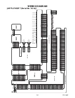
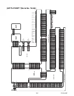
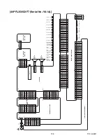
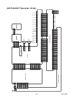
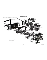
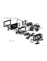
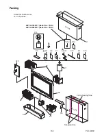
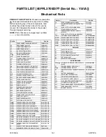
background image

20100406

14-2

A01P2EL

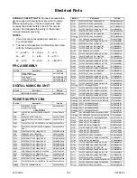
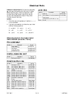
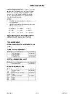
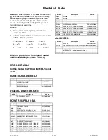
Electrical Parts

PRODUCT SAFETY NOTE:

 Products marked with a 

#

 have special characteristics important to safety. 

Before replacing any of these components, read 
carefully the product safety notice in this service 
manual. Don't degrade the safety of the product 
through improper servicing.

NOTES: 

1. Parts that are not assigned part numbers (---------) 

are not available.

2. Tolerance of Capacitors and Resistors are noted 

with the following symbols.

FRC ASSEMBLY

DIGITAL MAIN CBA UNIT

POWER SUPPLY CBA

C.....±0.25%

D.....±0.5%

F.....±1%

G.....±2%

J......±5%

K.....±10%

M.....±20%

N.....±30%

Z.....+80/-20%

Ref. No.

Description

Part No.

FRC ASSEMBLY
Consists of the following:

A01P2MFR-001

FRC CBA UNIT
FUNCTION CBA UNIT
IR SENSOR CBA UNIT

A01P2MFR-001-FR
A01P2MFR-001-FN
A01P2MFR-001-IR

Ref. No.

Description

Part No.

DIGITAL MAIN CBA UNIT

A01P2MMA-002

Ref. No.

Description

Part No.

POWER SUPPLY CBA
Consists of the following:

A01P0MPW-001

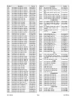
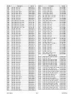
CAPACITORS

C603

POLYESTER FILM CAP. (PB FREE) 0.047

µ

F/

100V J

CA2A473DT018

C604

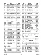
CERAMIC CAP. RB 100pF/2KV

CA3D101TE006

C605

POLYESTER FILM CAP. (PB FREE) 0.0015

µ

F/

100V J

CA2A152DT018

C606

POLYESTER FILM CAP. (PB FREE) 0.1

µ

F/100V 

J

CA2A104DT018

C607

POLYESTER FILM CAP. (PB FREE) 0.0022

µ

F/

100V J

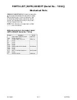
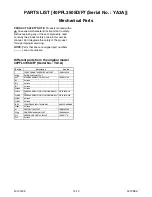
CA2A222DT018

C609

ELECTROLYTIC CAP. 1000

µ

F/25V M

CE1EMZNDL102

C651

CERAMIC CAP. BL 1500pF/2KV

CA3D152XF003

C652

ELECTROLYTIC CAP. 33

µ

F/50V M

CE1JMASDL330

C654

ELECTROLYTIC CAP. 1000

µ

F/35V M

CE1GMZNDL102

C657

ELECTROLYTIC CAP. 2200

µ

F/25V M

CE1EMZNDL222

C658

ELECTROLYTIC CAP. 2200

µ

F/25V M

CE1EMZNDL222

C659

ELECTROLYTIC CAP. 2200

µ

F/10V M

CE1AMZNDL222

C660

ELECTROLYTIC CAP. 1000

µ

F/10V M

CE1AMASDL102

C662

CHIP CERAMIC CAP.(1608) F Z 0.1

µ

F/50V

CHD1JZ30F104

C663

ELECTROLYTIC CAP. 1000

µ

F/10V M

CE1AMASDL102

C664

CHIP CERAMIC CAP.(1608) F Z 0.1

µ

F/50V

CHD1JZ30F104

C665

ELECTROLYTIC CAP. 1000

µ

F/6.3V M

CE0KMASDL102

C666

POLYESTER FILM CAP. (PB FREE) 0.1

µ

F/100V 

J

CA2A104DT018

C668

#

SAFTY CAP. 1000pF/250V KX

CA2E102MR101

C670

ELECTROLYTIC CAP. 1000

µ

F/6.3V M

CE0KMASDL102

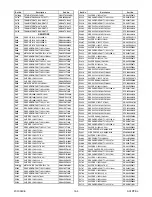
C1101

ELECTROLYTIC CAP. 100

µ

F/25V M

CE1EMASDL101

C1102

ELECTROLYTIC CAP. 1000

µ

F/16V M

CE1CMZNDL102

C1104

CHIP CERAMIC CAP.(1608) B K 0.1

µ

F/50V

CHD1JK30B104

C1105

ELECTROLYTIC CAP. 1

µ

F/50V M

CE1JMASDL1R0

C1106

CHIP CERAMIC CAP. B K 1200pF/50V

CHD1JK30B122

C1201

#

ELECTROLYTIC CAP 33

µ

F/200V M

CE2DMZNDL330

C1202

CAP CERAMIC HV 1000pF/1KV B K

CA3A102TE006

C1203

CHIP CERAMIC CAP.(1608) B K 0.22

µ

F/25V

CHD1EK30B224

C1204

ELECTROLYTIC CAP. 1

µ

F/50V M

CE1JMASDL1R0

C1205

CHIP CERAMIC CAP. B K 2200pF/50V

CHD1JK30B222

C1206

CHIP CERAMIC CAP. B K 330pF/50V

CHD1JK30B331

C1208

CAP CERAMIC SL J 15pF/2KV

CCD3DJNSL150

C1210

CHIP CERAMIC CAP.(1608) B K 0.1

µ

F/50V

CHD1JK30B104

C1401

CHIP CERAMIC CAP. B K 1200pF/50V

CHD1JK30B122

C1402

ELECTROLYTIC CAP. 4.7

µ

F/50V M

CE1JMASDL4R7

C1403

CHIP CERAMIC CAP.(1608) B K 0.22

µ

F/25V

CHD1EK30B224

C1404

CHIP CERAMIC CAP.(1608) B K 2.2

µ

F/10V

CHD1AK30B225

C1405

CHIP CERAMIC CAP. B K 1200pF/50V

CHD1JK30B122

C1406

CHIP CERAMIC CAP.(1608) B K 1000pF/50V

CHD1JK30B102

C1407

CHIP CERAMIC CAP. B K 1200pF/50V

CHD1JK30B122

C1408

ELECTROLYTIC CAP. 33

µ

F/50V M

CE1JMASDL330

C1409

CHIP CERAMIC CAP.(1608) B K 0.1

µ

F/50V

CHD1JK30B104

C1410

CHIP CERAMIC CAP.(1608) B K 0.022

µ

F/50V

CHD1JK30B223

C1411

ELECTROLYTIC CAP. 100

µ

F/25V M

CE1EMASDL101

C1412

CHIP CERAMIC CAP.(1608) B K 0.01

µ

F/50V

CHD1JK30B103

C1413

#

SAFTY CAP. 1000pF/250V KX

CA2E102MR101

C1414

CHIP CERAMIC CAP.(1608) B K 0.1

µ

F/50V

CHD1JK30B104

C1415

CHIP CERAMIC CAP.(1608) CH J 22pF/50V

CHD1JJ3CH220

C1416

CHIP CERAMIC CAP.(1608) CH J 22pF/50V

CHD1JJ3CH220

C1417

CHIP CERAMIC CAP.(1608) B K 0.1

µ

F/50V

CHD1JK30B104

C1601

#

CAP METALIZED FILM 1.0

µ

F/310V /K/LE-MX

CTA1050DC001

C1602

#

CAP METALIZED FILM 0.1

µ

F/310V /K/LE-MX

CTA1040DC001

C1603

#

SAFTY CAP. 1000pF/250V KX

CA2E102MR101

C1604

#

SAFTY CAP. 1000pF/250V KX

CA2E102MR101

C1605

#

SAFTY CAP. 1000pF/250V KX

CA2E102MR101

C1606

#

SAFTY CAP. 1000pF/250V KX

CA2E102MR101

C1607

CAP METALIZED FILM J1.0

µ

F/630V/J/MPEF

CA2K105DT048

C1610

#

CAP METALIZED FILM 0.22

µ

F/310V /K/LE-MX

CTA2240DC001

C1612

CAP ELECTROLYTIC 150

µ

F/400V/M/25/30

CA2H151DYG18

C1618

CERAMIC CAP. BL 1500pF/2KV

CA3D152XF003

C1620

CERAMIC CAP. BL 1500pF/2KV

CA3D152XF003

C1621

CERAMIC CAP. BL 1500pF/2KV

CA3D152XF003

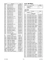
C1701

CHIP CERAMIC CAP.(1608) F Z 0.1

µ

F/50V

CHD1JZ30F104

C1702

CERAMIC CAP. RB 330pF/2KV

CA3D331TE006

C1703

CERAMIC CAP. RB 330pF/2KV

CA3D331TE006

C1704

ELECTROLYTIC CAP. 22

µ

F/50V M

CE1JMASDL220

C1705

CHIP CERAMIC CAP.(1608) B K 4700pF/50V

CHD1JK30B472

C1706

CERAMIC CAP. B K 100pF/1KV

CCD3AKD0B101

C1707

CHIP CERAMIC CAP.(1608) B K 0.1

µ

F/50V

CHD1JK30B104

C1708

CHIP CERAMIC CAP.(1608) F Z 0.1

µ

F/50V

CHD1JZ30F104

C1709

CHIP CERAMIC CAP. B K 330pF/50V

CHD1JK30B331

C1710

CHIP CERAMIC CAP.(1608) B K 0.1

µ

F/50V

CHD1JK30B104

C1711

CHIP CERAMIC CAP.(1608) B K 0.47

µ

F/16V

CHD1CK30B474

C1712

CHIP CERAMIC CAP.(1608) F Z 0.1

µ

F/50V

CHD1JZ30F104

C1713

ELECTROLYTIC CAP. 22

µ

F/50V M

CE1JMASDL220

C1714

CAP METALIZED FILM J0.039

µ

F/630V/J/MPEF CA2K393DT045

C1715

CHIP CERAMIC CAP.(1608) B K 4700pF/50V

CHD1JK30B472

C1716

ELECTROLYTIC CAP. 33

µ

F/50V M

CE1JMASDL330

Ref. No.

Description

Part No.

Summary of Contents for 40PFL3505D/F7

Page 1: ...ct to change without notice Funai reserves the right to change the content herein without the obligation to notify any person or organization of such changes with the design is a registered trademark of Funai Electric Co Ltd and may not be used in any way without the express written consent of Funai All other trademarks used herein remain the exclusive property of their respective owners Nothing c...

Page 2: ... equipment It also is important to understand that these CAUTIONS and NOTICES ARE NOT EXHAUSTIVE P F could not possibly know evaluate and advice the service trade of all conceivable ways in which service might be done or of the possible hazardous consequences of each way Consequently P F has not undertaken any such broad evaluation Accordingly a servicer who uses a service procedure or tool which ...

Page 3: ...abinet Disassembly Instructions 4 1 Electrical Adjustment Instructions 5 1 How to Initialize the LCD TV 6 1 Firmware Renewal Mode 7 1 Troubleshooting 8 1 Block Diagrams 9 1 Schematic Diagrams and Test Points 10 1 Waveforms 11 1 Wiring Diagram 12 1 Exploded Views 13 1 Parts List 14 1 Revision History 15 1 ...

Page 4: ...scription Condition Unit Nominal Limit 1 Native Pixel Resolution Horizontal Vertical pixels pixels 1920 1080 2 Brightness w filter cd m2 400 3 Viewing Angle Horizontal Vertical 88 to 88 88 to 88 70 to 70 70 to 70 Description Condition Unit Nominal Limit 1 Over Scan Horizontal Vertical 5 5 5 5 5 5 2 Color Temperature component1 x y K 12000 0 272 0 278 3 3 3 Resolution composite video Horizontal Ver...

Page 5: ...om any AC source connect an electrical jumper across the two AC plug prongs Place the instrument AC switch in the on position Connect one lead of an ohmmeter to the AC plug prongs tied together and touch the other ohmmeter lead in turn to each tuner antenna input exposed terminal screw and if applicable to the coaxial connector If the measured resistance is less than 1 0 megohm or greater than 5 2...

Page 6: ...m is not isolated from the AC power line The two ground systems are electrically separated by insulation material that must not be defeated or altered 5 Observe original lead dress Take extra care to assure correct lead dress in the following areas a near sharp edges b near thermally hot parts be sure that leads and components do not touch thermally hot parts c the AC supply d high voltage and e a...

Page 7: ...tubing 3 Spacers 4 Insulators for transistors E When replacing AC primary side components transformers power cord etc wrap ends of wires securely about the terminals before soldering F Observe that the wires do not contact heat producing parts heat sinks oxide metal film resistors fusible resistors etc G Check that replaced wires do not contact sharp edged or pointed parts H When a power cord has ...

Page 8: ...exposed accessible parts RF terminals antenna terminals video and audio input and output terminals microphone jacks earphone jacks etc is lower than or equal to the specified value in the table below Measuring Method Power ON Insert load Z between B earth ground power cord plug prongs and exposed accessible parts Use an AC voltmeter to measure across both terminals of load Z See Fig 2 and followin...

Page 9: ...the Flat Pack IC about 5 to 6 seconds Fig S 1 1 2 Remove the flat pack IC with tweezers while applying the hot air 3 Bottom of the flat pack IC is fixed with glue to the CBA when removing entire flat pack IC first apply soldering iron to center of the flat pack IC and heat up Then remove glue will be melted Fig S 1 6 4 Release the flat pack IC from the CBA using tweezers Fig S 1 6 CAUTION 1 The Fl...

Page 10: ...y one using a sharp pin or wire to which solder will not adhere iron wire When heating the pins use a fine tip soldering iron or a hot air desoldering machine Fig S 1 4 3 Bottom of the flat pack IC is fixed with glue to the CBA when removing entire flat pack IC first apply soldering iron to center of the flat pack IC and heat up Then remove glue will be melted Fig S 1 6 4 Release the flat pack IC ...

Page 11: ...ig S 1 6 Note When using a soldering iron care must be taken to ensure that the flat pack IC is not being held by glue When the flat pack IC is removed from the CBA handle it gently because it may be damaged if force is applied 2 Installation 1 Using desoldering braid remove the solder from the foil of each pin of the flat pack IC on the CBA so you can install a replacement flat pack IC more easil...

Page 12: ...d to remove any static electricity that may be charged on the body 2 Ground for Workbench Be sure to place a conductive sheet or copper plate with proper grounding 1 MΩ on the workbench or other surface where the semi conductors are to be placed Because the static electricity charge on clothing will not escape through the body grounding band be careful to avoid contacting semi conductors with your...

Page 13: ...eaker 15 FR PCB Holder 5 Stand Bracket 16 PCB Holder D U 17 Wall Mount Bracket L R 12 Digital Main CBA Unit 10 Jack CBA 14 FRC CBA Unit 13 Jack PCB Holder 19 LCD Module Assembly 20 Front Cabinet Assembly 6 IR Sensor CBA Unit 11 1 Junction CBA 7 Function CBA Unit 8 Front Flare 18 Side Holder L R 7 Function CBA Unit D2 D5 Function Knob Knob Frame Sheet Key 8 Front Flare D2 8 S 9 Boss S 9 Power Suppl...

Page 14: ...oved or installed 3 Fig No showing procedure of part location 4 Identification of parts to be removed unhooked unlocked released unplugged unclamped or desoldered P Spring L Locking Tab S Screw H Hex Screw CN Connector e g 2 S 2 two Screws of S 2 2 L 2 two Locking Tabs of L 2 5 Refer to the following Reference Notes in the Table 2 Rear Cabinet S 1 1 Stand Assembly S 2 S 2 S 2 S 2 S 2 S 2 S 3 Fig D...

Page 15: ...lare 7 Function CBA Unit 6 IR Sensor CBA Unit 5 Stand Bracket S 7 S 7 S 8 S 6 S 4 S 9 S 9 S 9 S 9 AC Inlet Holder Speaker Cushion Speaker Cushion Boss S Boss S Speaker Cushion Knob Frame Function Knob Sheet Key Sheet Sensor S 5 3 Speaker S 4 S 5 Speaker Cushion Fig D2 ...

Page 16: ... Digital Main CBA Unit 14 FRC CBA Unit S 14 S 14 S 18 S 17 S 15 S 16 S 18 S 18 S 19 S 14 S 13 S 12 S 11 S 10 S 10 Jack Holder A Shield Box Shield Box FR Jack Holder D 10 Jack CBA 11 1 Junction CBA 1 40PFL3705D F7 Serial No YA1A 9 Power Supply CBA Fig D3 ...

Page 17: ... Mount Bracket L 17 Wall Mount Bracket R 18 Side Holder R 19 LCD Module Assembly 20 Front Cabinet Assembly 18 Side Holder L 16 PCB Holder U 16 PCB Holder D S 23 S 23 S 20 S 20 S 21 S 21 S 22 S 23 S 23 S 22 S 21 S 21 Fig D4 ...

Page 18: ... Main CBA Unit Junction CBA 40PFL3705D F7 Serial No YA1A Function CBA Unit IR Sensor CBA Unit To LCD Module Assembly To AC Inlet To Speaker CN3701 CN3702 CN1914 CN1802 CN1801 CN1601 WH2101 CN2101 CN2103 CN2102 WH2102 CN2106 CN2104 CN2801 CN2802 CN5004 CN5003 CN5002 CN5001 FRC CBA Unit CN1803 Fig D5 ...

Page 19: ...Holder 3 Speaker 5 Stand Bracket 14 PCB Holder D U 15 Wall Mount Bracket L R 12 Digital Main CBA Unit 10 Jack CBA 13 Jack PCB Holder 17 LCD Module Assembly 18 Front Cabinet Assembly 6 IR Sensor CBA Unit 11 1 Junction CBA 7 Function CBA Unit 8 Front Flare 16 Side Holder L R 6 IR Sensor CBA Unit D2 D5 CN4051 CN4052 Sheet Sensor 7 Function CBA Unit D2 D5 Function Knob Knob Frame Sheet Key 8 Front Fla...

Page 20: ...ved or installed 3 Fig No showing procedure of part location 4 Identification of parts to be removed unhooked unlocked released unplugged unclamped or desoldered P Spring L Locking Tab S Screw H Hex Screw CN Connector e g 2 S 2 two Screws of S 2 2 L 2 two Locking Tabs of L 2 5 Refer to the following Reference Notes in the Table 2 Rear Cabinet S 1 1 Stand Assembly S 2 S 2 S 2 S 2 S 2 S 2 S 3 Fig D1...

Page 21: ...are 7 Function CBA Unit 6 IR Sensor CBA Unit 5 Stand Bracket S 7 S 7 S 8 S 6 S 4 S 9 S 9 S 9 S 9 AC Inlet Holder Speaker Cushion Speaker Cushion Boss S Boss S Speaker Cushion Knob Frame Function Knob Sheet Key Sheet Sensor S 5 3 Speaker S 4 S 5 Speaker Cushion Fig D2 ...

Page 22: ... Jack PCB Holder 12 Digital Main CBA Unit S 14 S 14 S 15 S 16 S 14 S 13 S 12 S 11 S 10 S 10 Jack Holder A Shield Box Jack Holder D 10 Jack CBA 9 Power Supply CBA 11 1 Junction CBA 1 40PFL3505D F7 Serial No YA1A Fig D3 ...

Page 23: ... Mount Bracket L 15 Wall Mount Bracket R 16 Side Holder R 17 LCD Module Assembly 18 Front Cabinet Assembly 16 Side Holder L 14 PCB Holder U 14 PCB Holder D S 20 S 20 S 17 S 17 S 18 S 18 S 19 S 20 S 20 S 19 S 18 S 18 Fig D4 ...

Page 24: ...N4052 Digital Main CBA Unit Junction CBA Function CBA Unit IR Sensor CBA Unit To LCD Module Assembly To LCD Module Assembly To AC Inlet To Speaker CN3701 CN3702 CN1914 CN1802 CN1801 CN1601 WH2101 CN2101 CN2103 CN2102 WH2102 CN2106 CN2104 CN2801 CN2802 40PFL3505D F7 Serial No YA1A Fig D5 ...

Page 25: ... on 2 Press MENU button to display Setup menu 3 Select Features 4 Select Current Software Info 5 Press 0 6 2 5 9 6 and Info buttons on the remote control unit in this order The following screen appears 1 Purity Check Mode This mode cycles through full screen displays of red green blue and white to check for non active pixels 1 Enter the Service mode 2 Each time the 7 button on the remote control u...

Page 26: ... select C D mode 5 CUTOFF Press 1 button to select COR for Red Cutoff adjustment Press 3 button to select COB for Blue Cutoff adjustment DRIVE Press 4 button to select DR for Red Drive adjustment Press 6 button to select DB for Blue Drive adjustment 6 In each color mode press CHANNEL UP DOWN buttons to adjust the values of color 7 Adjust Cutoff and Drive so that the color temperature becomes 12000...

Page 27: ...o put the program back at the factory default initialize the LCD TV using the following procedure 1 Turn the power on 2 Enter the service mode To cancel the service mode press POWER button on the remote control unit 3 Press INFO button on the remote control unit to initialize the LCD television 4 INITIALIZED will appear in the upper right of the screen INITIALIZED color will change to green from r...

Page 28: ...n the power off and turn the power on again Note When the Factory Upgrade is used after restarting TV shift to initial screen menu in service mode INITIALIZED will appear on the upper right of the screen INITIALIZED color will change to green from red when initializing is completed User Upgrade Upgrade the firmware only The setting values are not initialized Factory upgrade Upgrade the firmware an...

Page 29: ...Q601 Q602 Q1601 Q1602 T601 No Is the LCD 12V line voltage normal Yes Check each rectifying circuit of the secondary circuit and service it if defective Check the presence that the primary component is leaking or shorted and service it if defective Check the presence that the rectifying diode or circuit is shorted in each rectifying circuit of secondary side and service it if defective After servic...

Page 30: ...e it if defective Check if there is any leak or short circuit on the loaded circuit and service it if defective P ON 7 5V is not output Is approximately 8V voltage supplied to the cathode of D662 No Yes Check C659 D662 and their periphery circuit and service it if defective Check D2638 R2655 and their periphery circuit and service it if defective TUNER 35V is not output FLOW CHART NO 9 Is approxim...

Page 31: ...t if defective No Replace Q653 Q654 Check if there is any leak or short circuit on the loaded circuit and service it if defective LCD 12V is not output Is approximately 12V voltage supplied to the cathode of D672 No Yes Check C657 C658 D672 D673 D674 and their periphery circuit and service it if defective FLOW CHART NO 13 Check if there is any leak or short circuit on the loaded circuit and servic...

Page 32: ...le from the unit Check AL 3 3V line and service it if defective No Replace the remote control receiver RS4051 or the remote control unit Yes Replace Digital Main CBA Unit When pressing each switches SW4001 SW4006 do the voltage of Pin 25 of CN2103 increase Yes The key operation is not functioning FLOW CHART NO 1 Are the contact point and installation state of the key switches SW4001 SW4006 normal ...

Page 33: ...1 Yes No No No IC2701 VIDEO IN 1 3PIN IC2701 Y IN 1 1PIN IC2701 CVBS Y S Y OUT 38PIN IC2701 Pb OUT 36PIN IC2701 Pr S C OUT 34PIN IC2701 C IN 1 9PIN IC2701 VIDEO IN 2 7PIN IC2701 Y IN 2 5PIN IC2701 C IN 2 11PIN IC2701 COMPONENT Y IN 41PIN IC2701 COMPONENT Pb IN 45PIN IC2701 COMPONENT Pr IN VIDEO IN 1 Y IN 1 C IN 1 VIDEO IN 2 Y IN 2 C IN 2 COMPONENT Y IN COMPONENT Pb IN COMPONENT Pr IN 50PIN IC2701 ...

Page 34: ...ed to each pin of IC2701 Check the line between audio input terminal and each pin of IC2701 Are the audio L R signals outputted to Pin 27 28 of IC2701 Are the audio L R signals outputted to Pin 26 28 of CN2103 Yes No No No No Replace Digital Main CBA Unit Are the audio L R signals outputted to Pin 4 6 of CN2103 No IC2701 AUDIO L R IN 1 AUDIO L R IN 2 COMPONENT AUDIO L R IN HDMI AUDIO L R IN AUDIO ...

Page 35: ...Check the line between Pin 26 28 of CN2103 and Pin 19 32 of IC2801 and service it if defective Replace Digital Main CBA Unit Are the audio L R signals outputted to Pin 26 28 of CN2103 Replace Digital Main CBA Unit Are the audio L R signals outputted to Pin 4 6 of CN2103 Are the audio L R signals inputted to Pin 3 5 of IC2802 Check the line between Pin 4 6 of CN2103 and Pin 3 5 of IC2802 and servic...

Page 36: ... PROTECT3 21 21 BACKLIGHT SW 22 22 BACKLIGHT ADJ 7 7 RESET KEY IN1 25 25 Q2101 LIGHT SENSOR 1 1 LED R 5 5 REMOTE 23 23 P ON H2 10 10 P ON H2 R23 P ON H1 6 6 12 2 PROTECT3 10 4 BACKLIGHT SW 9 5 BACKLIGHT ADJ 8 6 POWER RESET P ON H1 6 8 P ON H2 7 7 TO AUDIO BLOCK DIAGRAM AUDIO MUTE AUDIO MUTE AB9 AE6 DRIVE 11 3 PROTECT1 PROTECT1 IR SENSOR CBA UNIT CN4052 REMOTE SENSOR RS4051 P ON 5V D4051 POWER IC40...

Page 37: ... S C IN 12 12 VIDEO INPUT SELECTOR WF1 WF2 WF3 C Y S VIDEO SW1 49 S VIDEO SW2 JK2706 S VIDEO IN2 C Y JK2707 VIDEO IN2 JK2702 S VIDEO IN1 JACK CBA CVBS Y S Y IN Pb IN Pr S C IN CN2102 CN3701 DIF OUT1 3 3 IF AGC 1 1 DIF OUT2 4 4 TO DIGITAL SIGNAL PROCESS BLOCK DIAGRAM DIF OUT1 DIF OUT2 IF AGC CN2103 CN3702 VIDEO SIGNAL AUDIO SIGNAL Either TU2301 is used for Jack CBA TU2301 DIF OUT1 11 DIF OUT2 12 TU...

Page 38: ...CL2802 SP2802 SPEAKER R CH IC3503 AUDIO D A CONVERTER IC3501 AUDIO DSP D A CONVERTER DSP L CH R CH 15 14 5 6 7 8 37 34 33 36 35 39 3 4 40 2 IC3502 AUDIO D A CONVERTER D A CONVERTER L CH R CH 15 14 5 6 7 8 CN2103 CN3702 CN2103 CN3702 AUDIO MUTE 14 14 JK2701 DIGITAL AUDIO OUT COAXIAL Q2701 BUFFER Q2804 Q2805 DRIVE Q2801 MUTE SPDIF 2 2 AUDIO L OUT 4 4 AUDIO R OUT 6 6 AMP L OUT 26 26 AMP R OUT 28 28 S...

Page 39: ...1 A11 HDMI1 SCL HDMI1 SDA B7 A7 LVDS TXB O4 19 LVDS TXB O4 20 LVDS TXB E1 13 LVDS TXB E1 14 LVDS TXB E0 15 LVDS TXB E0 16 LVDS TXB E2 11 LVDS TXB E2 12 LVDS TXB E3 5 LVDS TXB E3 6 LVDS TXB O0 31 LVDS TXB O0 32 LVDS TXB O1 29 LVDS TXB O1 30 LVDS TXB O2 27 LVDS TXB O2 28 LVDS TXB O3 21 LVDS TXB O3 22 LVDS TXB ECLK 8 LVDS TXB ECLK 9 LVDS TXB E4 3 LVDS TXB E4 4 LVDS TXB OCLK 24 LVDS TXB OCLK 25 S0 DQ ...

Page 40: ...A3 IF AGC HDMI2 SCL HDMI2 SDA HDMI IN1 JK3803 DATA0 DATA0 DATA1 DATA1 DATA2 DATA2 HDMI CLOCK HDMI DATA 7 9 4 6 1 3 10 12 15 16 CLOCK CLOCK DEMODULATOR MPEG DECODER AF2 AF7 AUDIO I F TO AUDIO BLOCK DIAGRAM ACLK ADATA1 BCLK LRCLK ADATA0 SPDIF AD14 AD9 AD12 AD10 AD11 AC10 HDMI I F D1 D2 C1 C2 B1 B2 A1 A2 DIF OUT1 DIF OUT2 IF AGC TO VIDEO BLOCK DIAGRAM AE2 M2 AUDIO R M1 AUDIO L VIDEO SIGNAL AUDIO SIGN...

Page 41: ...1 1 2 AC601 AC CORD AC INLET LINE FILTER L1601 LINE FILTER L1602 T1201 BRIDGE RECTIFIER D1201 D1204 BRIDGE RECTIFIER L1604 DRAIN VCC VDD FB TO SYSTEM CONTROL BLOCK DIAGRAM POWER SUPPLY CBA AL 4 3V 345V HOT 20V F1601 8A 250V 5 7 9 10 1 2 4 6 3 2 5 11 8 T1701 8 7 5 3 4 2 1 10 9 11 12 13 14 15 16 IC1202 1 4 3 2 IC1201 SWITCHING Q1602 SWITCHING Q1601 VCC SWITCHING FEED BACK RL1201 Q1202 Q1201 Q1701 SW...

Page 42: ...AM PROTECT1 6 8 2 3 LCD 12V P ON 3 5V LCD 12V P ON 3 3V P ON 7 5V P ON 5V P ON 3 3V JUNCTION CBA JACK CBA FRC CBA UNIT 10 P ON 3 5V 10 14 AMP 24V 14 1 TUNER 35V 1 CN1803 CN5001 3 4 LCD 12V 3 4 1 P ON 3 3V 1 P ON 3 3V 6 12 P ON 5V 12 P ON 7 5V 8 LCD 12V 2 3 WH2101 WH2102 6 8 2 3 10 P ON 3 5V 10 14 AMP 24V 14 1 TUNER 35V 1 P ON 3 3V 6 12 P ON 5V 12 P ON 7 5V 8 LCD 12V 2 3 Q653 Q654 SW 3 3V FEED BACK...

Page 43: ...1 SWITCHING CN1802 Q652 SW 5V TO SYSTEM CONTROL BLOCKDIAGRAM PROTECT1 6 8 2 3 LCD 12V P ON 3 5V LCD 12V P ON 3 3V P ON 7 5V P ON 5V P ON 3 3V JACK CBA FRC CBA UNIT 10 P ON 3 5V 10 14 AMP 24V 14 1 TUNER 35V 1 CN1803 CN5001 3 4 LCD 12V 3 4 1 P ON 3 3V 1 P ON 3 3V 6 12 P ON 5V 12 P ON 7 5V 8 LCD 12V 2 3 WH2102 Q653 Q654 SW 3 3V FEED BACK 345V HOT 20V 40PFL3705D F7 NOTE The voltage for parts in hot ci...

Page 44: ...fire or other hazards Notes 1 Do not use the part number shown on these drawings for ordering The correct part number is shown in the parts list and may be slightly different or amended since these drawings were prepared 2 All resistance values are indicated in ohms K 103 M 106 3 Resistor wattages are 1 4W or 1 6W unless otherwise specified 4 All capacitance values are indicated in µF P 10 6 µF 5 ...

Page 45: ...amended since the drawings were prepared 2 To maintain original function and reliability of repaired units use only original replacement parts which are listed with their part numbers in the parts list section of the service manual 4 Voltage indications on the schematics are as shown below Plug the TV power cord into a standard AC outlet 5 How to read converged lines 6 Test Point Information 2 3 1...

Page 46: ...50V fuse CAUTION ATTENTION Utiliser un fusible de rechange de même type de 8A 250V 8A 250V CAUTION Fixed voltage or Auto voltage selectable power supply circuit is used in this unit If Main Fuse F1601 is blown check to see that all components in the power supply circuit are not defective before you connect the AC plug to the AC power supply Otherwise it may cause some components in the power suppl...

Page 47: ...10 4 PL10 5SCP2 Power Supply 2 Schematic Diagram NOTE The voltage for parts in hot circuit is measured using hot GND as a common terminal ...

Page 48: ...10 5 PL10 5SCP3 Power Supply 3 Schematic Diagram NOTE The voltage for parts in hot circuit is measured using hot GND as a common terminal ...

Page 49: ...10 6 PL10 5SCJ1 Jack 1 Schematic Diagram ...

Page 50: ...10 7 PL10 5SCJ2 Jack 2 Junction Schematic Diagram ...

Page 51: ...10 8 PL10 5SCF Function Schematic Diagram ...

Page 52: ...10 9 PL10 5SCIR IR Sensor Schematic Diagram ...

Page 53: ...al Main 1 Schematic Diagram The order of pins shown in this diagram is different from that of actual IC3301 IC3301 is divided into five and shown as IC3301 1 5 IC3301 5 5 in this Digital Main Schematic Diagram Section 1 NOTE ...

Page 54: ...al Main 2 Schematic Diagram The order of pins shown in this diagram is different from that of actual IC3301 IC3301 is divided into five and shown as IC3301 1 5 IC3301 5 5 in this Digital Main Schematic Diagram Section 1 NOTE ...

Page 55: ...al Main 3 Schematic Diagram The order of pins shown in this diagram is different from that of actual IC3301 IC3301 is divided into five and shown as IC3301 1 5 IC3301 5 5 in this Digital Main Schematic Diagram Section 1 NOTE ...

Page 56: ...al Main 4 Schematic Diagram The order of pins shown in this diagram is different from that of actual IC3301 IC3301 is divided into five and shown as IC3301 1 5 IC3301 5 5 in this Digital Main Schematic Diagram Section 1 NOTE ...

Page 57: ...al Main 5 Schematic Diagram The order of pins shown in this diagram is different from that of actual IC3301 IC3301 is divided into five and shown as IC3301 1 5 IC3301 5 5 in this Digital Main Schematic Diagram Section 1 NOTE ...

Page 58: ...40PFL3705D F7 Serial No YA1A YA2A PL10 5SCFR1 The order of pins shown in this diagram is different from that of actual IC5001 IC5001 is divided into two and shown as IC5001 1 2 IC5001 2 2 in this FRC Schematic Diagram Section 2 NOTE ...

Page 59: ...40PFL3705D F7 Serial No YA1A YA2A PL10 5SCFR2 The order of pins shown in this diagram is different from that of actual IC5001 IC5001 is divided into two and shown as IC5001 1 2 IC5001 2 2 in this FRC Schematic Diagram Section 2 NOTE ...

Page 60: ... TUNER 35V HOT 17V J1016 CS J1015 J1084 HOT GND HOT GND J1105 HOT GND J1025 HOT GND J1024 HOT GND J1023 J1038 J1040 J1106 J1107 VINAC J1039 J1109 J1108 HOT GND HOT GND HOT GND HOT GND P ON3 5VforREG J1066 15 J1102 J1011 J1060 GND J1007 D1102 GND GND D1101 GND J1111 J1005 12 ALL 4 3V 13 ALL 4 3V C1209 D1206 ALL 4 3V 9 GND ALL 4 3V GND J1113 J1103 RL 5 0V J1114 RL 5 0V L1602 J1115 GND GND J1116 J112...

Page 61: ...V_DCDC HOT GND J1029 J1104 J1043 J1070 LCD 12V J1071 LCD 12V J1117 LCD 12V HOT 17V J1052 HOT GND J1127 J1110 GND HOT GND J1112 HOT GND J1031 D1801 GND J1097 J1130 D670 J1051 J1123 GND J1063 GND J1122 GND P ON 3 3V J1077 Q654 R676 R677 GND J1079 J1101 GND J1126 GND GND GND GND C1102 J1131 J1132 D1722 J1059 J1074 J1054 J1076 J1128 HOT GND SD INV 24V INV 24V ALL 4 3V J1134 GND J1034 HOT GND J1002 P O...

Page 62: ...J 2 2 6 7 J 2 2 7 0 J 2 2 7 5 J 2 2 7 7 J 2 2 7 8 J 2 2 8 1 J 2 2 8 2 J 2 2 8 3 J 2 2 8 4 J 2 2 8 5 J 2 2 8 7 J 2 2 9 4 J 2 2 9 6 J 2 2 9 8 J 2 3 0 0 J 2 3 0 1 J 2 3 0 3 J 2 3 0 4 J 2 3 0 5 J 2 3 0 6 J 2 3 0 7 J 2 3 0 8 J 2 3 0 9 J 2 3 1 1 J 2 3 1 4 J 2 3 1 5 J 2 3 1 7 J 2 3 1 8 J 2 3 1 9 J 2 3 2 1 J 2 3 2 2 J 2 3 2 4 J 2 3 0 2 J 2 2 9 2 J 2 2 9 0 J 2 2 0 7 K E Y I N 1 G N D G N D G N D 2 4 V f o ...

Page 63: ...K 2 8 0 1 J K 2 7 1 6 J K 2 8 0 2 J K 2 7 1 0 J K 2 7 2 0 J K 2 7 2 1 J K 2 7 1 1 G N D J 2 2 0 5 J 2 2 1 0 J 2 2 3 0 J 2 2 3 3 A L L 3 3 V D 2 4 0 7 D 2 4 0 5 R 2 6 3 4 J 2 3 4 1 J 2 2 5 0 V I D E O 2 J 2 2 5 2 S 1 C J 2 2 4 7 V 2 R J 2 2 0 9 P O N 1 1 V G N D J 2 2 1 2 J 2 2 3 7 J 2 2 0 3 G N D D 2 1 0 2 L I G H T S E N S C 2 1 2 3 J 2 2 0 1 G N D D 2 1 0 3 D 2 1 0 4 2 4 V f o r A M P G N D 2 4 ...

Page 64: ... 20ms WF1 Pin 8 of CN2103 S VIDEO Y S VIDEO Y 0 2V 0 2V 20 20ms S VIDEO C S VIDEO C 0 2V 0 2V WF3 Pin 12 of CN2103 20 20ms AUDIO AUDIO 1V 1V 0 5m 0 5ms COMPONENT Pr COMPONENT Pr 0 2V 0 2V 20 20ms ms COMPONENT Pb COMPONENT Pb 0 2V 0 2V 20 20ms Pin 10 of CN2103 WF2 COMPONENT Y COMPONENT Y 0 2V 0 2V 20 20ms VIDEO IN S VIDEO IN COMPONENT IN S VIDEO IN COMPONENT IN Pin 20 of CN2103 WF4 ...

Page 65: ...VDS TXA E3 LVDS TXA E3 GND LVDS TXA ECLK LVDS TXA ECLK GND LVDS TXA E2 LVDS TXA E2 LVDS TXA E1 LVDS TXA E1 LVDS TXA E0 22 24 LVDS TXA E0 25 GND 26 GND 27 LVDS TXA O4 28 LVDS TXA O4 29 LVDS TXA O3 CN5003 30 34 32 38 36 31 33 35 37 39 43 41 47 45 40 42 44 46 48 50 49 LVDS TXA O3 GND LVDS TXA OCLK LVDS TXA OCLK GND LVDS TXA O2 LVDS TXA O2 LVDS TXA O1 LVDS TXA O1 LVDS TXA O0 LVDS TXA O0 GND CTRL1 CTRL...

Page 66: ...XA E2 LVDS TXA E1 LVDS TXA E1 LVDS TXA E0 22 24 LVDS TXA E0 25 GND 26 GND 27 LVDS TXA O4 28 LVDS TXA O4 29 LVDS TXA O3 CN5003 30 34 32 38 36 31 33 35 37 39 43 41 47 45 40 42 44 46 48 50 49 LVDS TXA O3 GND LVDS TXA OCLK LVDS TXA OCLK GND LVDS TXA O2 LVDS TXA O2 LVDS TXA O1 LVDS TXA O1 LVDS TXA O0 LVDS TXA O0 GND CTRL1 CTRL2 CTRL3 CTRL4 NU NU NU NU NU NU 51 11 LVDS TXB E2 10 GND 9 LVDS TXB ECLK 14 L...

Page 67: ...UDIO MUTE AL 3 3V AL 3 3V SDA SCL GND AUDIO L GND AUDIO R REMOTE 22 24 24 LED1 NU 25 25 KEY IN1 26 26 AMP L OUT 27 27 GND 28 28 AMP R OUT 29 29 GND CL2102 CL2103 DIGITAL MAIN CBA UNIT CN2104 1 1 KEY IN1 3 3 P ON 5V 2 2 LED R 4 4 AL 3 3V 5 5 REMOTE 6 6 GND 7 7 LIGHT SENSOR CN4052 CL2801 CL2802 SP2801 SPEAKER L CH SP2802 SPEAKER R CH 1 CN2801 2 SP L SP L 1 CN2802 2 SP R SP R TUNER UNIT CN2102 CN3701...

Page 68: ...6 AMP L OUT 27 27 GND 28 28 AMP R OUT 29 29 GND CL2102 CL2103 DIGITAL MAIN CBA UNIT CN2104 1 1 KEY IN1 3 3 P ON 5V 2 2 LED R 4 4 AL 3 3V 5 5 REMOTE 6 6 GND 7 7 LIGHT SENSOR CN4052 CL2801 CL2802 SP2801 SPEAKER L CH SP2802 SPEAKER R CH 1 CN2801 2 SP L SP L 1 CN2802 2 SP R SP R TUNER UNIT CN2102 CN3701 CN2103 CN3702 CN3901 HDMI CONNECTOR 1 HDMI CONNECTOR 2 HDMI CONNECTOR 3 LCD MODULE ASSEMBLY CN3902 ...

Page 69: ...102 X3301 A11 L17 L17 B8 B9 B1 A2 L12 L5 L5 L5 L5 L5 L5 A9 L6 L17 L6 L6 L6 L6 L5 L5 L5 L5 B39 A5 A4 A16 CL2802 CL1601 See Electrical Parts List for parts with this mark Digital Main CBA Unit Power Supply CBA IR Sensor CBA Unit Function CBA Unit CL4001 SP2802 B33 B33 B33 B33 B11 B55 B40 B40 B40 B40 SP2801 CL2801 CL3101 CL3102 CL1914 L5 L5 L6 B2 B13 L6 B17 FRC CBA Unit X5002 CL1803 CL3100 L5 Jack CB...

Page 70: ...B39 X11 A22 L6 CL2103 CL2102 X3301 A11 L17 L17 B8 B9 B1 A2 L12 L5 L5 L5 L5 L5 L5 A9 L6 L17 L6 L6 L6 L6 L5 L5 L5 L5 B39 A5 A4 A16 CL2802 CL1601 See Electrical Parts List for parts with this mark Digital Main CBA Unit Power Supply CBA IR Sensor CBA Unit Function CBA Unit CL4001 SP2802 B33 B33 B33 B33 B11 B55 B40 B40 B40 B40 SP2801 CL2801 CL1914 CL3100 Jack CBA B14 B14 B20 B14 L3 L3 L3 L3 L3 Junction...

Page 71: ...g S2 Strapping Strip Carton Sealing Tape S1 X1 Some Ref Numbers are not in sequence S3 A22 X4 X3 L14 S6 S6 S4 FRONT FRONT X10 X8 X12 AC601 X7 X6 X2 S4 S5 S6 X15 X14 40PFL3705D F7 Serial No YA1A 40PFL3505D F7 Serial No YA1A ...

Page 72: ...A01P0 203 CL2102 WIRE ASSEMBLY 29PIN FFC 29PIN 50MM WX1A94H0 101 CL2103 WIRE ASSEMBLY 29PIN FFC 29PIN 50MM WX1A94H0 101 CL2106 WIRE ASSEMBLY 13PIN FFC 13PIN 120MM WX1A01P0 101 CL2801 WIRE ASSEMBLY 2PIN 2PIN 190MM WX1A01P0 211 CL2802 WIRE ASSEMBLY 2PIN 2PIN 720MM WX1A01P0 212 CL3100 LVDS WIRE ASSEMBLYS 51PIN 51PIN 170MM WX1A01P0 301 CL3101 LVDS WIRE ASSEMBLYS 51PIN 51PIN 215MM WX1A01P0 304 CL3102 L...

Page 73: ... C1205 CHIP CERAMIC CAP B K 2200pF 50V CHD1JK30B222 C1206 CHIP CERAMIC CAP B K 330pF 50V CHD1JK30B331 C1208 CAP CERAMIC SL J 15pF 2KV CCD3DJNSL150 C1210 CHIP CERAMIC CAP 1608 B K 0 1µF 50V CHD1JK30B104 C1401 CHIP CERAMIC CAP B K 1200pF 50V CHD1JK30B122 C1402 ELECTROLYTIC CAP 4 7µF 50V M CE1JMASDL4R7 C1403 CHIP CERAMIC CAP 1608 B K 0 22µF 25V CHD1EK30B224 C1404 CHIP CERAMIC CAP 1608 B K 2 2µF 10V C...

Page 74: ...TB033BST26 D1209 DIODE ZENER 39BSB T26 NDTB039BST26 D1210 DIODE ZENER 39BSB T26 NDTB039BST26 D1211 DIODE ZENER 39BSB T26 NDTB039BST26 Ref No Description Part No D1215 DIODE SWITCHING 1N4148 F0021 NDTZ01N4148F D1401 DIODE ZENER 18BSB T26 NDTB018BST26 D1402 DIODE ZENER HZS24NB3TE EQ QDTCHZS24NB3 D1603 DIODE ZENER 27BSB T26 NDTB027BST26 D1604 DIODE FAST RECOVERY 30PFB60 QDWZ030PFB60 D1605 DIODE ZENER...

Page 75: ...63 R1209 CHIP RES 1 10W J 6 8k Ω RRXAJR5Z0682 Ref No Description Part No R1210 CHIP RES 1 10W J 47k Ω RRXAJR5Z0473 R1214 RES CARBON FILM T 1 4W J 2 2 Ω RCX42R2T1001 R1216 RES CARBON FILM T 1 4W J 1 0k Ω RCX4102T1001 R1226 RES CARBON FILM T 1 4W J 4 7k Ω RCX4472T1001 R1401 RES CHIP 3216 1 4W F 825k Ω RTC8253HH020 R1402 RES CHIP 3216 1 4W F 825k Ω RTC8253HH020 R1403 RES CHIP 3216 1 4W F 619k Ω RTC61...

Page 76: ... No JACK ASSEMBLY Consists of the following A01P2MJC 001 JACK CBA JUNCTION CBA Ref No Description Part No JACK CBA Consists of the following CAPACITORS C2101 ELECTROLYTIC CAP 1µF 50V M CE1JMASDL1R0 C2102 CHIP CERAMIC CAP 1608 F Z 0 1µF 50V CHD1JZ30F104 C2103 CHIP CERAMIC CAP 1608 F Z 0 1µF 50V CHD1JZ30F104 C2104 CHIP CERAMIC CAP 1608 F Z 0 1µF 50V CHD1JZ30F104 C2105 CHIP CERAMIC CAP 1608 F Z 0 1µF...

Page 77: ...08 CH J 270pF 50V CHD1JJ3CH271 C2827 CHIP CERAMIC CAP 1608 CH J 270pF 50V CHD1JJ3CH271 C2828 ELECTROLYTIC CAP 100µF 16V M H7 CE1CMAVSL101 C2829 CHIP CERAMIC CAP 1608 F Z 0 1µF 50V CHD1JZ30F104 C2830 ELECTROLYTIC CAP 4 7µF 50V M H7 CE1JMAVSL4R7 C2831 ELECTROLYTIC CAP 4 7µF 50V M H7 CE1JMAVSL4R7 C2832 ELECTROLYTIC CAP 47µF 25V M H7 CE1EMAVSL470 C2833 ELECTROLYTIC CAP 47µF 25V M H7 CE1EMAVSL470 C2838...

Page 78: ...o R2801 CHIP RES 1 10W J 560 Ω RRXAJR5Z0561 R2802 CHIP RES 1 10W J 560 Ω RRXAJR5Z0561 R2803 CHIP RES 1 10W J 100k Ω RRXAJR5Z0104 R2804 CHIP RES 1 10W J 100k Ω RRXAJR5Z0104 R2805 CHIP RES 1608 1 10W 0 Ω RRXAZR5Z0000 R2806 CHIP RES 1608 1 10W 0 Ω RRXAZR5Z0000 R2807 RES CARBON FILM T 1 4W J 1 0k Ω RCX4102T1001 R2808 RES CARBON FILM T 1 4W J 1 0k Ω RCX4102T1001 R2809 CHIP RES 1608 1 10W 0 Ω RRXAZR5Z00...

Page 79: ...PCB S RED 01 RCA 101H RD JXRJ010YUQ01 TU2301 TUNER UNIT ATSC NTSC QAM TDYU4 D02A UTNATS0AL001 Ref No Description Part No JUNCTION CBA Consists of the following CONNECTOR CN2101 242SERIESCONNECTORTUC P15X B1WHT ST JCTUB15TG002 Ref No Description Part No ...

Page 80: ...er servicing NOTE Parts that are not assigned part numbers are not available Different parts from the original model 40PFL3705D F7 Serial No YA1A Ref No Description Part No CL1914 WIRE ASSEMBLY 14PIN 14PIN 240MM AWG 24 WX1A01P0 213 CL3101 WIRE ASSEMBLY LVDS51PIN 41PIN 41PIN 51PIN 280MM WX1A01P0 307 CL3102 WIRE ASSEMBLY LVDS 51PIN 41PIN 51PIN 41PIN 180MM WX1A01P0 308 LCD 1 LCD MODULE 40W LTA400HF08...

Page 81: ...L MAIN CBA UNIT A01PGMMA 002 Ref No Description Part No POWER SUPPLY CBA A01PGMPW 001 C1734 CAP CERAMIC HV 1000pF 1KV B K CA3A102TE006 C1735 CAP CERAMIC HV 1000pF 1KV B K CA3A102TE006 CN1802 CONNECTOR PRINT OSU B15B PH K S LF SN J3PHC15JG029 D656 DIODE SHOTTKY SB3200BR NDWZ3200D027 D1201 DIODE GENERAL PURPOSE 1N5406 BU NDLZ1N5406BU D1202 DIODE GENERAL PURPOSE 1N5406 BU NDLZ1N5406BU D1203 DIODE GEN...

Page 82: ...gh improper servicing NOTE Parts that are not assigned part numbers are not available Different parts from the original model 40PFL3705D F7 Serial No YA1A Ref No Description Part No FRONT CABINET ASSEMBLY A01PCUF 1EM025945A A12 RATING LABEL A01PCUF A22 STAND ASSEMBLY FIX A01P2UF 1EMN25479A B2 Not used B13 Not used B17 Not used CL1803 Not used CL3100 WIRE ASSEMBLY LVDS 51PIN 350MM WX1A01P0 306 CL31...

Page 83: ...ent parts from the original model 40PFL3705D F7 Serial No YA1A FRC ASSEMBLY In this model the FRC ASSEMBLY is not used FUNCTION ASSEMBLY DIGITAL MAIN CBA UNIT POWER SUPPLY CBA C 0 25 D 0 5 F 1 G 2 J 5 K 10 M 20 N 30 Z 80 20 Ref No Description Part No FUNCTION ASSEMBLY Consists of the following A01PCMSW 001 FUNCTION CBA UNIT IR SENSOR CBA UNIT A01PCMSW 001 FN A01PCMSW 001 IR Ref No Description Part...

Page 84: ... available Different parts from the original model 40PFL3705D F7 Serial No YA1A Ref No Description Part No FRONT CABINET ASSEMBLY A01PCUF 1EM025945A A12 RATING LABEL A01PCUF A22 STAND ASSEMBLY FIX A01P2UF 1EMN25479A B2 Not used B13 Not used B17 Not used CL1803 Not used CL1914 WIRE ASSEMBLY 14PIN 14PIN 240MM AWG 24 WX1A01P0 213 CL3100 WIRE ASSEMBLY 51PIN 51PIN 370MM UL1517 WX1A01P0 309 CL3101 Not u...

Page 85: ...n Part No POWER SUPPLY CBA A01PEMPW 001 C658 Not used C663 ELECTROLYTIC CAP 470µF 10V M CE1AMASDL471 C1734 CAP CERAMIC HV 1000PF 1KV B K CA3A102TE006 C1735 CAP CERAMIC HV 1000PF 1KV B K CA3A102TE006 CN1802 CONNECTOR PRINT OSU B15B PH K S LF SN J3PHC15JG029 CN1803 Not used D656 DIODE SHOTTKY SB3200BR NDWZ3200D027 D1201 DIODE GENERAL PURPOSE 1N5406 BU NDLZ1N5406BU D1202 DIODE GENERAL PURPOSE 1N5406 ...

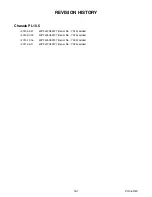
Page 86: ... REVISION HISTORY Chassis PL10 5 2010 04 21 40PFL3705D F7 Serial No YA1A added 2010 07 20 40PFL3505D F7 Serial No YA1A added 2010 12 16 40PFL3505D F7 Serial No YA3A added 2011 05 11 40PFL3705D F7 Serial No YA2A added ...

Page 87: ...PL10 5COM COMPARISON LIST OF MODEL NAME Chassis PL10 5 40PFL3705D F7 YA1A A01P2UF YA2A A01PGUF 40PFL3505D F7 YA1A A01PCUF YA3A A01PNUF ...

Reviews: