background image

Service Modes, Error Codes, and Fault Finding

EN 16

TPM9.1AL LA

5.

2012-Jun-15

back to 

div. table

How to Navigate

In the SAM menu, select menu items with the UP/DOWN 
keys on the remote control transmitter. The selected item 
will be indicated. When not all menu items fit on the screen, 
use the UP/DOWN keys to display the next/previous menu 
items.

With the “LEFT/RIGHT” keys, it is possible to:

(De) activate the selected menu item.

(De) activate the selected sub menu.

Change the value of the selected menu item.

When you press the MENU button once while in top level 
SAM, the set will switch to the normal user menu (with the 
SAM mode still active in the background). 

Press the following key sequence on the remote control 
transmitter: “062596” directly followed by the “Home” 
button to switch to SDM (do not allow the display to time out 
between entries while keying the sequence). 

How to Store SAM Settings
To store the settings changed in SAM mode (except the 
RGB Align settings), leave the top level SAM menu by using 
the POWER button on the remote control transmitter or the 
television set. The mentioned exceptions must be stored 
separately via the STORE button.

How to Exit SAM
Use one of the following methods:

Switch the set to STANDBY by pressing the mains button 
on the remote control transmitter or the television set.

Via a standard RC-transmitter, key in “00” sequence.

Note: When the TV is switched “off” by a power interrupt while 
in SAM, the TV will show up in “normal operation mode” as 
soon as the power is supplied again. The error buffer will not be 
cleared.

5.2.4

Contents of the Factory mode:

Purpose

To perform extended alignments.

Specifications

Displaying and or changing Panel ID information.

Displaying and or changing Tuner ID information.

Error buffer clearing.

Various software alignment settings.

Testpattern displaying.

Public Broadcasting Service password Reset.

etc.

How to Activate the Factory mode
To activate the Factory mode, use the following method:

Press the following key sequence on the remote control 
transmitter: from the “Home screen” press “1999”, directly 
followed by the “Back” button. Do not allow the display to 
time out between entries while keying the sequence.

After entering the Factory mode, the following items are 
displayed, 

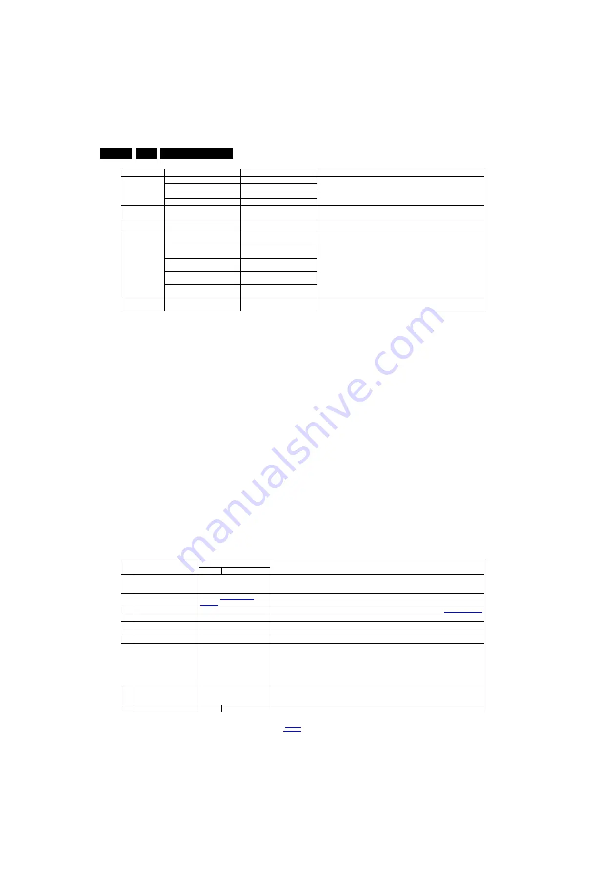
Table 5-2 Factory mode overview

Download from USB Copy Channel List from USB

To download several settings from the USB stick to the TV

Copy NVM from USB

Copy Readable Info from USB

Copy EDID from USB

Initialize NVM

Press [OK] to Initialize NVM 
immediately

To initialize a (corrupted) NVM. Be careful, this will erase all settings.

EDID Write Enable

Press [OK] to enable EDID writable 
immediately

Enable EDID for writing

Service Data

Type Number

Press [OK] use key pad edit type 
number immediately

Edit and display the applicable service data by using the displayed key pad.

Production Number

Press [OK] use key pad edit 
production number immediately

12NC SSB

Press [OK] use key pad edit SSB 
immediately

12NC PSU

Press [OK] use key pad edit PSU 
immediately

12NC Display

Press [OK] use key pad edit display 
immediately

Clear OAD Version

Press [OK] to clean OAD Version 
immediately

Clean OAD (Over Air Download, firmware update method) Version

Main Menu

Sub-menu 1

Sub-menu 2

Description

Item Item value

Default value

Description

32"

42"

0

F/W VERSION

Press OK

Displays the software versions of the supplier, Flash PQ, Smart Picture, BL Dimming, Source Meter, the 
Picture Quality checksum, the Dimming library, the Source meter library, the Flash AQ, the MTK, MCU and 
OAD software versions.

1

Panel_ID

See table 

6-3 Display code 

overview

Displays and changes the Panel ID with the left and right cursor; be careful changing this, it can result in not 
correct displaying the screen!

2

ERR Code: xxx xxx xxx xxx xxx 000 000 000 000 000

Values showing the last 5 errors during the last 50 hours of operation, according to table 

5-4 Error code table

3

CLEAR ERROR BUFFER

Press OK

Selecting this clear all current error codes.

4

NVM ADDRESS

0

NVM address 0 to 8191, Use Item 6 to change and 7 to store the data to the correct NVM address

5

NVM VALUE

various

Displays the value at the NVM address of item 5

6

NVM STORE

Press OK

Use this option to save the data of item 6 to NVM address of item 5

7

NVM COPY TV to USB

Press OK

Use this to store the NVM data to the REPAIR folder of a FAT formatted USB memory stick. The TV will write 
two files in the REPAIR folder of the memory stick. It will create this folder if it does not exist. The items are 
“Channel list”, “Personal settings”, “Option codes”, “Display-related alignments” and “History list”. In case the 
download to the USB stick was not successful “Failure” will appear. In this case, check if the USB stick is 
connected properly. Now the settings are stored onto the USB stick and can be used to download onto another 
TV or other SSB. Uploading is of course only possible if the software is running and if a picture is available. 
This method is created to be able to save the customer’s TV settings and to store them into another SSB.

8

NVM COPY USB to TV

Press OK

Use this to store the NVM data from the USB memory stick to the TV. The TV will save the two files which were 
created in item 8 to the NVM of the set. Use these options when replacing a SSB. When “USB to TV Success” 
is displayed remove the power and restart the TV

9

CLR_TEMP_R

139

140

Red colour temperature setting

Summary of Contents for 32PFL3007

Page 1: ...PS Shield Emblem are used under license from Koninklijke Philips Electronics N V Colour Television Chassis TPM9 1A LA Contents Page 1 Revision List 2 2 Technical Specs Diversity and Connections 2 3 Precautions Notes and Abbreviation List 5 4 Mechanical Instructions 9 5 Service Modes Error Codes and Fault Finding 14 6 Alignments 24 7 Circuit Descriptions 26 8 IC Data Sheets 30 9 Block Diagrams Wiri...

Page 2: ...ions and software drivers Table 2 1 Described Model Numbers and Diversity 2 2 Directions for Use Directions for use can be downloaded from the following websites http www philips com support http www p4c philips com CTN 2 4 9 10 11 Connection Overview Mechanics Block Diagrams Schematics Styling Wire Dressing Rear Cover Removal SSB Removal Wiring Diagram Block Diagram SSB J IR LED E Keyboard Leadin...

Page 3: ...MS 10 k jq Wh Audio L 0 5 VRMS 10 k jq 5 HDMI 3 Digital Video In Digital Audio In Out Figure 2 3 HDMI type A connector 1 D2 Data channel j 2 Shield Gnd H 3 D2 Data channel j 4 D1 Data channel j 5 Shield Gnd H 6 D1 Data channel j 7 D0 Data channel j 8 Shield Gnd H 9 D0 Data channel j 10 CLK Data channel j 11 Shield Gnd H 12 CLK Data channel j 13 Easylink CEC Control channel jk 14 n c 15 DDC_SCL DDC...

Page 4: ... sync 0 5 V j 15 DDC_SCL DDC clock j 9 HDMI 2 Digital Video In Digital Audio with ARC In Out See 5 HDMI 3 Digital Video In Digital Audio In Out 10 HDMI 1 Digital Video In Digital Audio with ARC In Out See 5 HDMI 3 Digital Video In Digital Audio In Out 11 Cinch Video CVBS Out Audio Out Ye Video CVBS 1 VPP 75 kq Rd Audio R 0 5 VRMS 10 k kq Wh Audio L 0 5 VRMS 10 k kq 12 Service UART 1 UART_TX Transm...

Page 5: ...carrier at 475 25 MHz for PAL or 61 25 MHz for NTSC channel 3 Where necessary measure the waveforms and voltages with D and without E aerial signal Measure the voltages in the power supply section both in normal operation G and in stand by F These values are indicated by means of the appropriate symbols 3 3 2 Schematic Notes All resistor values are in ohms and the value multiplier is often used to...

Page 6: ...are sometimes held in less regard Always respect voltages While some may not be dangerous in themselves they can cause unexpected reactions that are best avoided Before reaching into a powered TV set it is best to test the high voltage insulation It is easy to do and is a good service precaution 3 4 Abbreviation List 0 6 12 SCART switch control signal on A V board 0 loop through AUX to TV 6 play 1...

Page 7: ...f the International Telecommunication Union relating to radio communication ITU 656 a k a SDI is a digitized video format used for broadcast grade video Uncompressed digital component or digital composite signals can be used The SDI signal is self synchronizing uses 8 bit or 10 bit data words and has a maximum data rate of 270 Mbit s with a minimum bandwidth of 135 MHz iTV Institutional TeleVision...

Page 8: ...Serial Clock I2C SCL F CLock Signal on Fast I2 C bus SD Standard Definition SDA Serial Data I2C SDA F DAta Signal on Fast I2 C bus SDI Serial Digital Interface see ITU 656 SDRAM Synchronous DRAM SECAM SEequence Couleur Avec Mémoire Colour system mainly used in France and East Europe Colour carriers 4 406250 MHz and 4 250000 MHz SIF Sound Intermediate Frequency SMPS Switched Mode Power Supply SoC S...

Page 9: ...tions Index of this chapter 4 1 Cable Dressing 4 2 Service Positions 4 3 Assembly Panel Removal 4 4 Set Re assembly Notes Figures below can deviate slightly from the actual situation due to the different set executions 4 1 Cable Dressing Figure 4 1 Cable dressing 32 19330_100_120608 eps 120608 ...

Page 10: ...e guidelines can seriously damage the display Ensure that ESD safe measures are taken 4 3 Assembly Panel Removal Instructions below apply to the 32PFL3507H 12 but will be similar for other models 4 3 1 Rear Cover Refer to Figure 4 3 for details Warning Disconnect the mains power cord before removing the rear cover 1 Remove fixation screws 1 2 and 3 that secure the rear cover 2 At the top side the ...

Page 11: ...oval 4 3 2 Stand Refer to Figure 4 4 for details 1 Remove fixation screws 4 that secure the base assembly pull the base assembly downwards away from the catches Do not release the two screws in the middle of the stand 19330_102_120612 eps 120612 1 M4 8 Q4 16 1 1 1 1 1 1 2 2 2 2 2 2 2 2 2 2 2 Q3 8 3 3 ...

Page 12: ...ount all different screws at their original position during re assembly Failure to do so may result in damaging the SSB 1 Release the clips from the LVDS cable connector that connects the panel to the SSB 1 Caution be careful as these are very fragile connectors 2 Release the clamps and unplug all other connectors 2 3 Remove all the fixation screws from the SSB 3 4 Take out the SSB with I O bracke...

Page 13: ...nit 4 3 8 LCD Panel 1 Remove the SSB as described earlier 2 Remove the PSU as described earlier 3 Remove the speakers as described earlier 4 Remove the keyboard control unit as described earlier 5 Remove the IR LED board as described earlier 6 Remove all other metal parts that do not belong to the LCD panel 7 Release all fixing clips that secure the front bezel to the LCD panel 8 Lift the LCD Pane...

Page 14: ...l Next items are applicable to all Service Modes or are general Life Timer During the life time cycle of the TV set a timer is kept called Op Hour It counts the normal operation hours not the Stand by hours The actual value of the timer is displayed in SDM and SAM in a decimal value Every two soft resets increase the hour by 1 Stand by hours are not counted Software Identification Version and Clus...

Page 15: ...menu as soon as the power is supplied again The error buffer will not be cleared 5 2 3 Service Alignment Mode SAM Purpose To modify the NVM To display clear the error code buffer To perform alignments Specifications Operation hours counter maximum five digits displayed Software version error codes and option settings display Error buffer clearing Option settings Software alignments White Tone NVM ...

Page 16: ...s EDID Write Enable Press OK to enable EDID writable immediately Enable EDID for writing Service Data Type Number Press OK use key pad edit type number immediately Edit and display the applicable service data by using the displayed key pad Production Number Press OK use key pad edit production number immediately 12NC SSB Press OK use key pad edit SSB immediately 12NC PSU Press OK use key pad edit ...

Page 17: ...2 AUD_GAIN_USB 2 USB audio gain 43 TUNER_ID 167 Displays and changes the Tuner ID with the left and right cursor Not to be changed when the tuner is replaced with the correct service part 44 ESTICKER NVM1 3 3 ESTICKER value 45 ESTICKER NVM2 6 4 ESTICKER value 46 ESTICKER NVM3 7 6 ESTICKER value 47 ESTICKER NVM4 8 7 ESTICKER value 48 ESTICKER NVM5 9 8 ESTICKER value 49 ESTICKER NVM6 10 9 ESTICKER v...

Page 18: ...duction code the serial number of the TV Note that if an NVM is replaced or is initialized after corruption this production code has to be re written to NVM 1 3 Installation date Indicates the date of the first installation of the TV This date is acquired via time extraction 1 4 Option Code 1 Gives the option codes of option group 1 as set in SAM 1 5 Option Code 2 Gives the option codes of option ...

Page 19: ...ital background tasks completed Swith On previously in Standby Semi Standby Mains Power Plug Standby Soft Mode Command Received Power tact switch Switch Off Mains Power Plug Switch Off Mains Power Plug Swith On previously in Standby Soft Mode Mains Power Plug Standby commands Received RC Standby key Standby Soft Mode Command Received previously in Standby Soft Mode Power tact switch TV Wakeup comm...

Page 20: ...products and it s recommend that the TV software is updated when updates are available Software update files can be obtained from the dealer or can be downloaded from the following websites http www philips com support Preparing a portable memory for software upgrade The following requirements have to be met 1 A personal computer connected to the internet 2 An archive utility that supports the ZIP...

Page 21: ...ted SW protection Failing I2 C device General I2 C error The last five errors stored in the NVM are shown in the Service menu s This is called the error buffer The error code buffer contains all errors detected since the last time the buffer was erased The buffer is written from left to right When an error occurs that is not yet in the error code buffer it is displayed at the left side and all oth...

Page 22: ...entered 5 8 Fault Finding and Repair Tips Note It is assumed that the components are mounted correctly with correct values and no bad solder joints Before any fault finding actions check if the correct options are set 5 8 1 NVM Editor In some cases it can be convenient if one directly can change the NVM contents This can be done with the NVM Editor in SAM mode With this option single bytes can be ...

Page 23: ...012 Jun 15 back to div table 5 8 10 Display option code Attention In case the SSB is replaced always check the Panel Code in CSM even when picture is available Performance with the incorrect display option code can lead to unwanted side effects for certain conditions ...

Page 24: ...en as input signal and set the following values Red BL Offset and Green BL Offset to 7 if present All White point values initial to 128 In case you have a colour analyser Measure with a calibrated phosphor independent color analyser e g Minolta CA 210 in the centre of the screen Consequently the measurement needs to be done in a dark environment Adjust the correct x y coordinates while holding one...

Page 25: ...tool or use the NVM editor and Dealer options items in SAM do not forget to store After a repaired SSB has been mounted in the set set repair on board level the type number CTN and production code of the TV has to be set according to the type plate of the set For this you can use the NVM editor in SAM The loading of the CTN and production code can also be done via ComPair Model number programming ...

Page 26: ...ck see chapter 9 Block Diagrams and circuit diagrams see chapter 10 Circuit Diagrams and PWB Layouts Where necessary you will find a separate drawing for clarification 7 1 Introduction The TPM9 1A LA series is a new chassis launched in Asia in 2012 the whole range is covered by MT5301BGMU B LQFP 256 main IC so called MT5301 platform Philips 3007 series comes with the following stylings Philips 300...

Page 27: ...7 TPM9 1AL LA 7 2012 Jun 15 back to div table 7 1 3 SSB Cell Layout Figure 7 1 SSB layout cells top view 19330_200_120611 eps 120612 DC DC ANALOG I O TUNER CVI AV MT5301B HDMI SWITCH HDMI HDMI USB Headphone DDR DDR AV IN AV OUT ...

Page 28: ...ly units is mainly determined by the diversity in displays The following displays can be distinguished CCFL backlight power board is conventional IPB LED backlight side view LED without scanning PSL power board side view LED with scanning PSLS power board direct view LED without 2D dimming PSL power board direct view LED with 2D dimming PSDL power board PSL stands for Power Supply with integrated ...

Page 29: ...rcuit DDC repeater function 2 mW low power mode Local I2 C or GPIO configurable in this application the default I2C addresses is 0x58 7 6 Video and Audio Processing MT5301B The MT5301B is the main audio and video processor or System on Chip for this platform It has the following features Worldwide multi standard analog TV demodulator A transport demultiplexer A multi standard video decoder An AC3 ...

Page 30: ...m 19160_300_110622 eps 120612 Block diagram MT5301BCMU JPEG MP2 MP 4 DivX H 264 V C 1 RM AVS Component Analog Input 16 bit DDR2 DDR3 DRAM Bus JTAG IO Bus USB2 0 UART I 2 C PWM IrDA PCR SDIO Audio DSP NTSC PAL SECAM ATD Watchdog CVBS YC Input Audio I F SPDIF Out I2 S RTC 2 D Graphic OSD scaler VADCx4 TV Decoder HDMI In I F LVDS OD mini LVDS TCON Audio Input Mix and Post Processing DDR2 DDR3 Control...

Page 31: ... AO2N 30 163 Y0P AO1P 31 162 SOY0 AO1N 32 161 PR1P AO0P 33 160 PB1P AO0N 34 159 COM1 VCCK 35 158 Y1P VCCK 36 157 SOY1 VCCK 37 156 RP AVDD12_MEMPLL 38 155 COM AVSS12_MEMPLL 39 154 GP RODT RCKE 40 153 SOG RA8 RA10 41 152 BP RA13 RBA1 42 151 HSYNC RA11 RA4 43 150 VSYNC RA4 RA1 44 149 AVDD33_VGA_STB RA6 RA6 45 148 AVDD10_LDO RA0 RA8 46 147 ADIN4_SRV RA2 RA11 47 146 ADIN3_SRV RCAS_ RA12 48 145 ADIN2_SR...

Page 32: ...S I S _ A D S K N S _ D P H K N I 1 S L C S 48 47 46 45 44 43 42 41 40 39 38 37 36 35 34 33 D2 _1 D2 _1 VCC D1 _1 D1 _1 GND D0 _1 D0 _1 VCC CLK _1 CLK _1 SCL1 SDA1 HPD1 I2C_SEL S2 SDA 4 6 3 6 2 6 1 6 0 6 9 5 8 5 7 5 6 5 5 5 4 5 53 2 5 1 5 0 5 9 4 D P H 3 2 D 2 _ 2 _ 2 D V C C 1 D 2 _ 2 _ 1 D D N G 0 D 2 _ 2 _ 0 D V C C K L C 2 _ K L C 2 _ 2 L C S S 2 A D D P H 2 P L TMDS361B HPD_SINK Vcc RINT Cloc...

Page 33: ... diagram Pinning information 1 HPVDD CPP INL INL INR INR PGND CPN 2 3 4 12 11 10 9 16 15 14 13 5 6 7 8 OUTR G0 G1 HPVSS OUTL SGND VDD EN TPA6132A2RTER Click and Pop Suppression HPVDD HPVSS HPVDD HPVSS Charge Pump INR INR INL INL OUTL OUTR CPP CPN HPVSS G0 EN Thermal Protection Gain Select G1 VDD Supply Control PGND SGND HPVDD Resistor Array 1 F 1 F 2 2 F Short Circuit Protection Resistor Array HPV...

Page 34: ...5 6 7 8 9 10 11 12 36 35 34 33 32 31 30 29 28 27 26 25 37 38 39 40 41 42 43 44 45 46 47 48 24 23 22 21 20 19 18 17 16 15 14 13 RA N C GNDR N C RB VDDRB VDDLB LB N C GNDL N C LA VDDLA N C N C N C N C PLL MCLK CLK_OUT DGND DVDD DEF SDATA SCL SUBB SUBA SA1 SA0 RESET ERROR PD BCLK LRCIN CFG1 CFG0 AD82586 SA1 Input Interface I2 C Control Interface PCM to PWM Loudspeaker Driver L R BCLK SDATA LRCIN ERRO...

Page 35: ...orkshops MAIN POWER SUPPLY 1054 A to panel CN901 L N LOUDSPEAKER LOUDSPEAKER 1185 1185 LOUDSPEAKER LOUDSPEAKER 1185 1185 IR LED BOARD 1056 J 5P KEYBOARD CONTROL 1057 SSB 1053 B 40P 13P 13P 13P CN904 to panel CN902 CN701 CN408 CN401 CN601 CN01 4P CN01 TV ANTENNA Y V Pb Pr L R Y Pb Pr L R CVI 2 AV AV OUT VIDEO L R CVI 1 AUDIO VGA HDMI 2 HDMI 1 SERV U HDMI 3 VIDEO AV IN 1 L R USB 1 USB 2 E LOUDSPEAKE...

Page 36: ...OWER SUPPLY 1054 A CN901 L N LOUDSPEAKER LOUDSPEAKER 1185 1185 LOUDSPEAKER LOUDSPEAKER 1185 1185 IR LED BOARD 1056 J 5P KEYBOARD CONTROL 1057 SSB 1053 B 13P CN01 4P CN01 TV ANTENNA Y V Pb Pr L R Y Pb Pr L R CVI 2 AV AV OUT VIDEOLR CVI 1 AUDIO VGA HDMI 2 HDMI 1 SERV U HDMI 3VIDEO AV IN 1 LR USB 1 USB 2 to panel to panel CN801 CN802 CN902 13P CN701 4P CN601 13P CN401 to panel 40P CN408 Component Lev...

Page 37: ...NVM 24C128 D A RF TUNER UART KEY RC 24C02 24C02 AUDIO AMP SPK AD82586 CVBS 2 CVBS 2 CVI DDC PC IN Digital Audio Output COAXIAL HDMI1 RGB YPbPr HDMI2 24C02 24C02 SPDIF TMDS361B DDC DDC HDMI3 I2 S LVDS 50 60 Hz RX0 RX3 LCD PANEL USB1 2 0 USB2 2 0 R L IN 4052 Audio in MUX A RF TUNER MT5301B DDC Digital IF Demodulator ATBM8846E DDC DDC NAND FLASH 32MB TS PARALLEL HeadPhone Out ATV Demodulator ...

Page 38: ...N 14 AE1P 15 AE1N 16 AE0P 17 AE0N 18 AVDD33_LVDSA 19 AVDD33_LVDSA 20 AO5P 21 AO5N 22 AO4P 23 AO4N 24 AO3P 25 AO3N 26 AOCKP 27 AOCKN 28 AO2P 29 AO2N 30 AO1P 31 AO1N 32 AO0P 33 AO0N 34 VCCK 35 VCCK 36 VCCK 37 AVDD12_MEMPLL 38 AVSS12_MEMPLL 39 RODT RCKE 40 RA8 RA10 41 RA13 RBA1 42 RA11 RA4 43 RA4 RA1 44 RA6 RA6 45 RA0 RA8 46 RA2 RA11 47 RCAS_ RA12 48 RCS_ RRAS_ 49 RRAS_ RCAS_ 50 RA9 RWE_ 51 VCC2IO 52...

Page 39: ...09 100N 16V R4117 4K7 1 16W 5 R4110 NC 100K 1 16W 5VSB 3V3SB DVDD3V3 3V3SB DVDD3V3 DVDD3V3 3V3SB 3V3SB OPCTRL4 4 OPCTRL5 4 AOSDATA1 4 MEMORY_WP 4 GND 4 6 7 8 9 10 11 12 13 14 15 16 17 18 19 20 21 22 23 24 OSDA0 4 7 12 14 15 20 OSCL0 4 7 12 14 15 20 POWE 4 PAALE 4 PACLE 4 POCE1 4 POOE 4 PARB 4 OXTALI 4 OXTALO 4 ORESET 4 PDD0 4 PDD1 4 PDD2 4 PDD3 4 PDD4 4 PDD5 4 PDD6 4 PDD7 4 NC23 39 NC1 1 NC2 2 NC3...

Page 40: ..._7 G1 DQL7 H7 VDDQ_6 F1 DQL1 F7 VDDQ_7 H2 DQL0 E3 VDDQ_8 H9 DQL4 H3 VSSQ_8 G9 DQL3 F8 DQL2 F2 BA2 M3 DQL5 H8 VDD_5 N1 VREFDQ H1 VSS_2 E1 VSS_5 J8 CK J7 VDD_2 G7 CKE K9 WE L3 RAS J3 CK K7 ODT K1 RESET T2 BA0 M2 BA1 N8 CAS K3 CS L2 A10 AP L7 A1 P7 A2 P3 A0 N3 VDD_3 K2 VSS_3 G8 A3 N2 A5 P2 A6 R8 A4 P8 A7 R2 A9 R3 A11 R7 A8 T8 VSS_4 J2 VDD_4 K8 A12 N7 NC_3 L9 ZQ L8 NC_2 L1 VREFCA M8 NC_4 M7 NC T3 NC_6...

Page 41: ...1 3 3K 1 16W 1 2 3 4 5 6 7 8 9 10 11 12 13 14 15 16 17 18 19 20 21 22 23 24 25 26 27 28 29 30 CN409 NC CONN R416 1K 1 16W 5 R405 NC 1K 1 16W 5 R410 33R 1 16W 5 Q401 NC 2N7002 R413 10K 1 16W 5 R402 0R05 1 16W R415 10K 1 16W 5 1 2 3 CN410 CONN R420 100R 1 16W 5 R411 10K 1 16W 5 R419 3 3K 1 16W R414 10K 1 16W 5 R403 NC 1K 1 16W 5 R418 10K 1 16W 5 Q402 NC 2N7002 C402 100N 50V R417 10K 1 16W 5 C403 100...

Page 42: ...B2 C1003 100N 16V R1001 NC 0R05 1 16W OUT 1 GND 2 FAULT 3 EN 4 IN 5 U1001 NC STMPS2171STR C1005 NC 4P7 50V R1003 NC 4K7 1 16W 5 C1004 NC 4P7 50V C1002 47UF 25V VUSB5V VUSB1_5V DVDD3V3 C1001 NC 100N 16V VUSB1_5V USB_DP0 USB_DM0 USB_DP1 USB_DM1 USB_DM0 DVDD3V3 USB_DP0 USB_PWR_OCP0 H POWER ON L POWER OFF USB1_D USB1_D USB_PWR_EN0 USB1 H OK L O C R1008 0R05 1 16W R1010 NC 15K 1 16W 5 R1009 NC 15K 1 16...

Page 43: ...6 10K 1 16W 5 R112 470K 1 16W 5 C106 NC 220pF 50V Q101 PMBS3904 R110 470K 1 16W 5 2 1 4 3 5 6 A B C CN121 RCA JACK C112 10U 16V C102 100N16V R109 5 1K 1 C111 10U 16V 1 2 FB114 120R 3000mA C101 10U 16V R107 10K 1 16W 5 R103 75R 1 16W 1 R126 10K 1 16W 5 AMUX_5V AMUX_5V AMUX_5V AMUX_5V AV1 Input Side 5V_SW AMUX_5V GND 4 5 6 7 8 10 11 12 13 14 15 16 17 18 19 20 21 22 23 24 CVBS_COM 4 AV1_CVBS 4 CVI_R_...

Page 44: ...138 10N 50V C130 10U 16V R138 56R 1 16W 5 R152 100R 1 16W 5 R150 56R 1 16W 5 C123 10N 50V R139 68R 1 16W 5 R161 470K 1 16W 5 R134 56R 1 16W 5 R157 10K 1 16W 5 R144 5 1K 1 R158 10K 1 16W 5 R143 5 1K 1 EXT_R R218 18R 1 16W 5 C143 10U 16V C134 10N 50V C122 10N 50V R147 470K 1 16W 5 R163 470K 1 16W 5 AMUX_5V AMUX_5V GND 4 5 6 7 8 9 11 12 13 14 15 16 17 18 19 20 21 22 23 24 Y1P 4 SOY1 4 Y0P 4 COM1 4 PB...

Page 45: ...1 Q105 PMBS3904 R196 0R05 1 10W 1 2 FB111 120R 3000mA R169 68R 1 16W 5 R194 NC 1K1 16W R223 4K7 1 16W 5 R181 0R05 1 16W BP RP SOG VGACOM GP C155 10U 16V R171 75R 1 16W 1 I O1 1 GND 2 I O2 3 I O3 4 VDD 5 I O4 6 U105 AOZ8105CI C144 NC 10P 50V C157 100N 16V C147 1 5nF 50V R197 0R05 1 10W R189 NC 0R05 1 16W R192 10K 1 16W 5 E0 1 E1 2 E2 3 VSS 4 SDA 5 SCL 6 WC 7 VCC 8 U104 M24C02 WDW6P R193 10K 1 16W 5...

Page 46: ...3 VSS 4 SDA 5 SCL 6 WC 7 VCC 8 U502 M24C02 WDW6P R518 1K 1 16W 5 R517 4K7 1 10W 5 R519 10K 1 10W R507 0R05 1 16W R505 1K 1 16W 5 R523 NC 0R05 1 16W Q501 PMBS3904 R522 NC 0R05 1 16W C504 100N 16V R501 100R 1 16W 5 C509 100N 16V R512 10K 1 10W 1 2 3 4 8 7 6 5 RP502 NC 0OHM 1 16W CEC_B CEC_A HDMI_CEC CEC_C D505 BAT54C C503 10U 16V C507 100N 16V CH1 1 CH2 2 VN 3 CH3 4 CH4 5 NC 6 NC 7 VN 8 NC 9 NC 10 U...

Page 47: ...XC_2 HDMIC_SDA HDMIC_SCL CEC_C RXC_C RXC_C HPD_C RXB_0 RXB_0 CEC_B RXB_2 RXB_2 RXB_1 RXB_1 RXB_C RXB_C 1 2 D512 AZ5125 01J PWR5V_B 1 2 ZD505 AZ5125 01J H Write L WP R553 10K 1 10W 1 2 ZD506 AZ5125 01J H Write L WP 1 2 D513 AZ5125 01J 1 2 D514 AZ5125 01J HD5V_B 1 2 D515 AZ5125 01J R546 470K 1 16W 5 R538 4K7 1 16W 5 C516 100N 16V Q508 PMBS3904 R536 100R 1 16W 5 R533 0R05 1 10W R556 1K 1 16W 5 R545 1...

Page 48: ...200R 1 16W 5 TP05 C1120 NC 100N16V IVINN TP06 C1129 NC 22pF 50V R1107 NC 100K 1 16W TP07 C1112 NC 100N16V C1121 NC 100N16V TESTIO21 SCLM ASIC_3V3 SDAM VDD33 R4147 NC 33R 1 16W 5 V3 3 VDD12 AVDD1V2 V1 2 ASIC_3V3 SDAM V3 3 AVDD33 VDD33 V3 3 VDD33 V3 3 AVDD33 DEMOD_TSSYNC 4 DEMOD_RESET 4 DEMOD_TSVALID 4 PWM0 DEMOD_TSDATA0 4 DEMOD_TSCLK 4 OSDA0 4 5 7 12 15 20 TU_SCL 15 OSCL0 4 5 7 12 15 20 T2D_TIF 15 ...

Page 49: ...RF_AGC_S2T R1162 0R05 1 10W L1111 0U10 H R1198 NC 4K7 1 16W 5 C1152 10N 50V R1144 NC 0R05 1 16W OSDA0 OSCL0 IF_AGC_D2T IF_AGC_S2T DTMB_PAL_SW R1142 NC 0R05 1 16W L1114 0 22uH 10 Q1103 2N7002 1 2 3 Q1106 NC PMBS3906 R1139 100R 1 16W 5 R1143 4K7 1 16W 5 L1108 NC 150uH C1155 220pF 50V C1139 100uF 25V Q1107 NC PMBS3904 R1146 NC 0R05 1 16W C1153 10N 50V B_5V B_5V B_5V B_5V 5V_SW 5V_TUNER TU_5V_SCL B_5V...

Page 50: ... 5 Q606 PMBS3904 C603 100N 50V R624 2 2K 1 16W R665 NC 100R 1 16W 5 C604 1uF 16V R625 10K 1 16W 5 R619 10K 1 16W 5 1 2 3 Q609 PMBS3906 R626 1K 1 16W 5 R638 47K 1 16W 5 R622 100R 1 16W 5 R623 470OHM1 10W R628 10K 1 16W 5 R621 470K 1 16W 5 D601 NC 1N4148W Q607 PMBS3904 D602 BAT54C R630 NC 100R 1 16W 5 Q605 PMBS3904 1 2 3 Q603 PMBS3906 Q602 PMBS3904 R627 1K 1 16W 5 R618 47K 1 16W 5 R629 1K 1 16W 5 R6...

Page 51: ...R 1 16W 5 3V3SB_2 TOC_KEY H OFF L ON Q201 NC 2N7002 C203 100N 16V 1 2 3 4 5 6 7 8 9 10 11 12 13 CN401 CONN Link to IR Keypad panel R220 0R05 1 10W 1 2 FB201 120R 3000mA R207 0R05 1 16W C205 100N 16V R211 0R05 1 16W R201 3 9K 1 C201 100N 16V C206 100N 16V R202 100R 1 16W 5 1 2 FB202 120R 3000mA R206 NC 4K7 1 16W 5 C202 100N 16V R208 0R05 1 16W 5VSB_2 3V3SB_2 3V3SB_2 3V3SB_2 3V3SB_2 3V3SB 5VSB_2 5VS...

Page 52: ...05 1 16W R1197 2K 1 16W 5 C1172 1N 50V R1184 15K 1 16W 5 C1171 100N 16V C1165 220pF 50V R1175 9K1 1 16W 5 R1189 0R05 1 10W R1182 9K1 1 16W 5 R1172 NC 100K 1 16W R1165 0R05 1 16W R1190 0R05 1 10W C1183 10N 50V R1179 1 02K 1 10W 1 C1175 1uF 16V C1166 220pF 50V R1174 NC 100K 1 16W C1169 10U 16V C1182 10N 50V R1186 47K 1 16W 5 R1173 5K1 1 16W 5 R1181 47K 1 16W 5 2 1 4 3 5 6 A B C CN1101 RCA JACK R1196...

Page 53: ...C611 1N 50V 1 2 ZD602 VPORT0603100KV05 1 2 ZD603 VPORT0603100KV05 R667 NC 0R05 1 16W C650 100N16V C610 1N 50V C606 10U 16V R632 0R05 1 16W R644 4K7 1 16W 5 C609 2 2nF 50V INL 1 INR 3 INL 2 OUTL 16 HPVDD 12 HPVSS 8 G0 6 INR 4 OUTR 5 CPP 11 CPN 9 EN 13 SGND 15 AVDD 14 PGND 10 G1 7 Thermal Pad 17 U606 TPA6132A2RTER C614 1uF 16V R684 0R05 1 16W C655 10N 50V R641 100R 1 16W 5 AR1O AL1O R633 10K 1 16W 5...

Page 54: ...V R670 NC 10K 1 16W 5 C639 1N 50V 1 2 3 4 5 6 CN601 CONN C624 100N 50V R657 10 OHM 1 10W C626 100N 50V C638 220N 50V 1 2 FB604 120R 3000mA R672 NC 10K 1 16W 5 C648 1N 50V R674 NC 10K 1 16W 5 R660 10 OHM 1 8W R661 10 OHM 1 10W R682 0R05 1 10W R675 100K 1 16W AMP_SA0 R663 NC 240 OHM 5 1 16W C652 NC 100P 50V C634 100N 50V L604 56UH 1 2 FB606 120R 3000mA R647 0R05 1 10W R646 0R05 1 10W C629 1UF 10V 1 ...

Page 55: ...8 9 10 11 12 13 14 15 16 17 18 19 20 22 23 24 PSU_STBY 4 22 DVDD3V3 PSU_STBY R4056 100R 1 16W 1 Reserved for OPWRST control PSU_STBY 5V_SW PWR_OK R701 10K 1 16W 5 R750 0R05 1 10W PSU_STBY PWR_OK 4 PWR_OK BL_DIM_PWM BL_ON OFF 0 Max Luma BL_DIM_PWM 99 Min Luma OPWRSB BL_CTRL BRI_ADJ R4055 NC 100R 1 16W 1 PSU_STBY OPWRSB OPWRSB 4 23 LIPS Interface H ON L Standby C703 330UF 35V C701 330UF 35V Brightne...

Page 56: ...Q706 PMBS3904 1 3 ZD702 NC BAT54 R723 10K 1 4W R717 10K 1 16W 5 S 1 S 2 S 3 G 4 D 8 D 7 D 6 D 5 Q709 AO4449 7A 30V S 1 S 2 S 3 G 4 D 8 D 7 D 6 D 5 Q707 AO4449 7A 30V 1 2 FB707 NC 120R 6000mA C713 100N 50V 1 2 FB708 120R 6000mA R724 1K 1 16W 5 1 2 FB712 NC 120R 6000mA C762 220NF 25V R727 10K 1 10W C714 220NF 25V R725 56KOHM 1 16W 1 2 FB709 NC 120R 6000mA Q704 PMBS3904 12V 5VSB 5V_BUCK 24V_12V_SW LV...

Page 57: ... 120R 3000mA 3V3_BUCK Soc Core Power 1 15V 3A C744 180P 50V VCC 1 REF 2 GND 3 FB 4 EN 5 PGND 6 LX 7 VIN 8 E PAD 9 U701 AT1529F11U VCC 1 REF 2 GND 3 FB 4 EN 5 PGND 6 LX 7 VIN 8 E PAD 9 U702 AT1529F11U C734 1uF 25V C730 1uF 50V R4152 2 7K 1 R4151 3Kohm 1 16W 1 C731 1uF 50V C735 100N 50V L704 4 7UH R4150 10R 1 16W 5 5V_SW R753 0R05 1 16W 1 2 FB720 NC 120R 3000mA C738 NC 1UF 10V 1 2 FB722 NC 120R 3000...

Page 58: ...2 R1 Analog Power AVDD1V2 Demod 1V2 Power V1 2 C756 1UF 10V 1 2 FB731 120R 3000mA C750 1UF 10V C759 1UF 10V VIN 3 VOUT 2 GND 1 4 4 U705 1 2 FB732 120R 3000mA 1 2 FB727 120R 3000mA C752 10U 16V 1 2 FB728 120R 3000mA VI 3 VO 2 GND 1 4 4 U708 1 2 FB734 120R 3000mA C751 10U 16V VIN 3 VOUT 2 GND 1 4 4 U707 C761 NC 10U 16V C757 10U 16V 1 2 FB733 120R 3000mA C760 10U 16V C758 NC 10U 16V 3V3SB 5VSB AVDD1V...

Page 59: ...06 R710 R165 R166 R649 R627 R636 R637 R150 R638 R704 R705 R706 R708 R726 R4144 R539 FDT1 FDT2 FDT4 FDT5 FDT6 FDT7 FDT8 R171 R540 R541 FDT9 FDT10 FDT11 FDT12 CN701 U704 U4104 U501 CN409 C1001 C1006 C1008 C108 C1128 C1129 C1142 C1143 C1159 C1145 C1150 C1151 C1154 C1158 C607 C1168 C4125 C1171 C654 C650 C128 C133 C146 C150 C153 C154 C202 C206 C4001 C4002 C1167 C4105 C4106 C4123 C617 C618 C628 C629 C65...

Page 60: ...N406 R110 R119 R120 R128 R157 R509 R510 R511 R629 R685 R668 R622 R116 R118 R126 R122 R131 R195 R185 R192 R193 R194 R1116 R1186 R620 R624 R4134 R4152 R132 R117 R191 R1114 R160 R621 R724 C141 R522 R1115 C630 R4151 R4141 FDT3 FDT13 FDT14 C1003 C1004 C1005 C1009 C1010 C1147 C1148 C1163 C1165 C1172 C4104 C4108 C4109 C508 C627 C743 C744 C745 FB1107 FB1108 FB1109 FB1111 FB1112 FB502 FB717 FB719 FB731 FB7...

Page 61: ...R LED board 1 2 3 4 5 6 7 CN01 CONN Q002 NC PMBT3904 R003 NC 2 2K1 16W VCC R007 NC 2 2K1 16W R005 NC 2 2K1 16W BLUE VCC RED 1 2 3 Q1 NC PMBS3906 R006 NC 1K 1 10W 1 R002 1K 1 10W 1 R004 1K 1 10W 1 LED_B 1 2 ZD2 NC RLZ5 6B R001 2K7 1 16W 5 C01 100N 50V GND 1 GND 2 OUT 3 VCC 4 U01 IRM H936M3 TR2 1 3 2 UB SUR LED1 R008 220R 1 C03 1UF 10V 033G8032 5F HR 1 3 ZD3 BZX84 C5V1 C02 NC 4 7UF VCC 1 GND1 GND PI...

Page 62: ...iv table 10 2 2 IR LED Board layout 19330_524_120608 eps 120611 2012 03 20 X 715G5324 IR LED board layout top bottom C01 C02 R006 R004 R002 R2 R1 CN01 GND1 GND2 R003 ZD2 LED1 R005 R007 Q002 Q1 R001 U01 C03 R008 ZD3 Layout IR LED Board Top Side Layout IR LED Board Bottom Side ...

Page 63: ...EY 33G8032 4F HR MENU Source Select Power ON OFF VOL VOL CH CH R05 750OHM 1 1 8W R04 1K 1 8W 1 R01 7K5 1 8W 1 R03 1K8 1 1 8W R07 750OHM 1 1 8W R02 2K7 1 1 8W R08 750OHM 1 1 8W SW01 TACT SW FWRD H1 5MM 1 2 3 4 6 5 CN01 CONN C01 NC FUNC_KEY C07 NC C05 NC C03 NC C06 NC C02 NC C04 NC PWR SW 77G 607 2 FD SW02 TACT SW FWRD H1 5MM SW03 TACT SW FWRD H1 5MM SW04 TACT SW FWRD H1 5MM SW05 TACT SW FWRD H1 5MM...

Page 64: ...3 2 Keyboard layout 19330_526_120608 eps 120611 2010 01 29 C 715G3814 Keyboard layout top bottom C02 R08 R01 R02 R03 R04 R05 R07 C05 C06 C07 C04 C03 C01 CN20 CN21 R2 SW04 SW01 SW02 SW03 SW05 SW06 SW07 CN01 SW1 SW2 SW3 SW4 SW5 SW6 SW7 Layout Key Board Top Side Layout Key Board Bottom Side ...

Page 65: ...Description Remarks 0030 Base 0031 Front bezel 0041 Rear cover 0050 Stand base Assembly 1050 Display panel 1053 Panel SSB 1054 Power Supply Unit 1056 IR LED panel 1057 Keyboard control panel 1176 Remote control Not displayed 1185 Speakers FOR ELECTRICAL PARTS ASSEMBLIES SEE WIRING DIAGRAM CHAPTER 9 0030 0050 0041 1054 1185 1185 0031 1050 1053 1056 1057 ...

Page 66: ...L PARTS ASSEMBLIES SEE WIRING DIAGRAM CHAPTER 9 Pos No Description Remarks 0030 Base 0031 Front bezel 0041 Rear cover 0050 Stand assembly 1050 Display panel 1053 Panel SSB 1054 Power Supply Unit 1056 IR LED panel 1057 Keyboard control panel 1176 Remote control Not displayed 1185 Speakers 0030 0050 0041 1054 1185 1185 0031 1050 1053 1057 1056 ...

Reviews: