


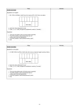
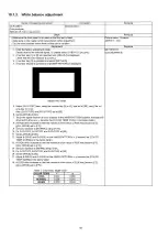


10.1.3. White balance adjustment
Name o f m easuring instrum ent
Connection
Remarks
W / B pattern
Color analyzer
(Minolta CA-100 or equivalent)
Panel surface
Steps
Rem arks
Make sure the front panel to be used on the final set is fitted.
Make sure a color signal is not being shown before adjustment.
Put the color analyzer w here there is little colour variation.
Picture menu : Dynamic
A S PE C T : 16:9
A djustm ent
Remarks
1. Enter the factory adjustm ent mode.
Please receive the external signal. Or, please select C VB S/Y U V (no sync).
2. A num ber key [1] or [2] are operated and [W B-ADJ] is displayed.
Check that the color balance is [ COOL ].
3. A num ber key [0] is operated and select [METHOD].
4. A num ber key [5] is operated and [INNER PATTERN] is displayed.
METHOD=01
copy adjustm ents
5. Select [G -CUTO FF] item, using the number-key [3] or [4], and set to [80], using the v o l
um e-key [+] or [-].
Also, [B-CUTO FF] and [R-CUTO FF] set to [80]
6. Set [G -DRIVE] at [D0].
7. Touch the signal receiver o f color analyzer to the INNER PATTERN's center, and adjust B
drive and R drive so x, y become the [COLOR TEM P COOL] in the below ta b le 1 .
8. All RGB drive increase so that the m aximum drive value o f RGB may become [FF].
([ALL-D RIVE] set to [FF].)
Set color balance to [NORM AL] using [7] key.
Fix G-CUTOFF, B-CUTOFF and R-CUTOFF at [80].
Set [G -D RIVE] at [D0].
12. Adjust B-DRIVE and R-DRIVE so the INNER PATTERN's x, y become the [COLOR
TEM P NORMAL] in the below table1.
13. All RGB drive increase so that the m aximum drive value o f RGB may become [FF].
([ALL-D RIVE] set to [FF].)
Set color balance to [WARM] using [7] key.
Fix G-CUTOFF, B-CUTOFF and R-CUTOFF at [80].
16. Set [G -D RIVE] at [D0].
17. Adjust B-DRIVE and R-DRIVE so the INNER PATTERN's x, y become the [COLOR
TEM P W ARM] in the below table1.
All RGB drive increase so that the m aximum drive value o f RGB may become [FF].
([ALL-D RIVE] set to [FF].)
9
10
11
14
15
18
32
Summary of Contents for Viera TX-P42S20L
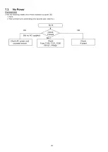
Page 21: ...7 4 No Picture 21...
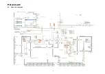
Page 33: ...11 Block Diagram 11 1 Main Block Diagram 33...
Page 34: ...11 2 Block 1 4 Diagram 34...
Page 35: ...G 0 11 3 Block 2 4 Diagram I A I D IG IT A L S IG N A L P R O C E S S O R 35...
Page 36: ...11 4 Block 3 4 Diagram P P O W E R S U P P LY 36...
Page 37: ...11 5 Block 4 4 Diagram s c s c a n d r i v e s s s u s t a i n d r i v e 37...
Page 38: ...38...
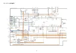
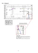
Page 40: ...12 3 Wiring 2 40...
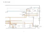
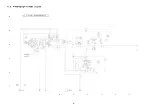
Page 43: ...13 2 P Board 1 4 Schematic Diagram A B C D E A P BO ARD LSEP1287BE HB 1 4 F 1 2 3 4 42...
Page 44: ...13 3 P Board 2 4 Schematic Diagram A P BO ARD LSEP1287BE HB 2 4 10 11 12 13 14 15 16 17 18 43...
Page 45: ...13 4 P Board 3 4 Schematic Diagram A B C D E F 1 2 3 4 44 5...
Page 46: ...13 5 P Board 4 4 Schematic Diagram 10 11 12 13 14 15 16 17 18 45...
Page 47: ...13 6 A Board 1 19 Schematic Diagram A A A BO AR D 1 19 IIC B C D E F 1 2 3 4 9 46...
Page 52: ...13 11 Board 6 19 Schematic Diagram A A BO AR D 6 19 STB MPU 46 47 48 49...
Page 54: ...13 12 Board 7 19 Schematic Diagram A A BO AR D 7 1 9 HDMI 55 56 57 58 59 52...
Page 57: ...69 70 71 72...
Page 59: ...Peaks COM MON 78 79 80 81...
Page 61: ...13 16 A Board 11 19 Schematic Diagram A A BO AR D 11 19 A V SW 91 92 93 94 95 96 97 98 99 56...
Page 63: ...FE_Virtual_Module Peaks COMMON TO 3 19 Analog ASIC 104 105 106 107 108 57...
Page 68: ...140 141 142 143 144 61...
Page 71: ...63...
Page 72: ...13 24 A Board 19 19 Schematic Diagram A A BO AR D 19 19 DVB T C D EM O D U LATO R 64...
Page 75: ...13 27 C2 Board 1 2 Schematic Diagram A A C 2 BO AR D TN PA5095 1 2 ___ I TO A BOARD A32 B 67...
Page 78: ...13 30 SC Board 2 4 Schematic Diagram 10 I 11 1 12 1 13 1 14 1 15 1 16 1 17 1 18 70...
Page 79: ...13 31 SC Board 3 4 Schematic Diagram 19 1 20 1 21 1 22 1 23 1 24 1 25 1 26 1 27 71...
Page 80: ...13 32 SC Board 4 4 Schematic Diagram 28 29 30 31 32 33 34 35 36 72...
Page 86: ...P BOARD COMPONENT SIDE LSEP1287BEHB B G 6 5 4 3 2 1 E F H 77...
Page 92: ...14 6 SC Board SC BOARD FOIL SIDE TXNSC11DEK B G 6 5 4 3 2 1 E F H 83...
Page 93: ...SC BOARD COMPONENT SIDE TXNSC11DEK B G 6 5 4 3 2 1 E F H 84...
Page 94: ...14 7 SS Board SS BOARD FOIL SIDE TXNSS11DEK B G 6 5 4 3 2 1 E F H 85...
Page 95: ...SS BOARD COMPONENT SIDE TXNSS11DEK...
Page 96: ......
Page 98: ...15 1 2 Exploded View 2 88...
Page 99: ...15 1 3 Packing 1 89...
Page 100: ...15 1 4 Packing 2 90...


