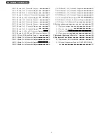
7.14. Exchange of the SU-Board and the SD-Board
16
7.15. Exchange of the SC-Board
16
7.16. Exchange of the SS2-Board and the SS3-Board
17
7.17. Exchange of the SS-Board
17
7.18. Exchange of the C1, C2, C3-Board
18
7.19. Exchange of the C4, C5, C6-Board
18
7.20. Exchange of the Fan
19
7.21. Exchange of the Escutcheon
20
7.22. Exchange of the Plasma Panel
21
8 Location of Lead Wiring
27
9 Adjustment Procedure
29
9.1.
Driver Set-up
29
9.2.
Initialization Pulse Adjust
30
9.3.
P.C.B. (Printed Circuit Board) exchange
31
9.4.
Adjustment Volume Location
31
9.5.
Test Point Location
31
10 Service mode
32
10.1. CAT (computer Aided Test) mode
32
10.2. IIC mode structure (following items value is sample data.)
34
11 Alignment
35
11.1. PC / RGB / NTSC / PAL / DVI panel white balance
35
11.2. HD / 525i / 525p / 625i / 625p panel white balance
38
12 Trouble shooting guide
40
12.1. Self Check
40
12.2. No Power
41
12.3. No Picture
42
12.4. Local screen failure
42
13 Option Setting
43
13.1. How to access and setting
43
13.2. Contents of Option Menu
44
14 Circuit Board Layout
45
14.1. PF-Board
45
14.2. PC-Board
46
14.3. P(SS)-Board
47
14.4. P(SC)-Board
50
14.5. F-Board
53
14.6. HA-Board(TH-65PHD7UY only)
54
14.7. HB-Board(TH-65PHD7UY only)
55
14.8. HX-Board
56
14.9. J-Board
57
14.10. D-Board
58
14.11. C1-Board
60
14.12. C2-Board
61
14.13. C3-Board
62
14.14. C4-Board
63
14.15. C5-Board
64
14.16. C6-Board
65
14.17. SC-Board
66
14.18. SU-Board
69
14.19. SD-Board
70
14.20. SS-Board
71
14.21. SS2 and SS3-Board
74
14.22. Z-Board
75
14.23. H3, S1 and V1-Board
77
15 Schematic Diagrams
79
15.1. Schematic Diagram Notes
79
15.2. Main Block Diagram
80
15.3. PF and F-Board Block Diagram
81
15.4. PF and F-Board Schematic Diagram
82
15.5. PC-Board Block Diagram
83
15.6. PC-Board Schematic Diagram
84
15.7. P(SS)-Board Block Diagram
85
15.8. P(SC)-Board Block Diagram
86
15.9. P(SS)-Board (1 of 6) Schematic Diagram
87
15.10. P(SS)-Board (2 of 6) Schematic Diagram
88
15.11. P(SS)-Board (3 of 6) Schematic Diagram
89
15.12. P(SS)-Board (4 of 6) Schematic Diagram
90
15.13. P(SS)-Board (5 of 6) Schematic Diagram
91
15.14. P(SS)-Board (6 of 6) Schematic Diagram
92
15.15. P(SC)-Board (1 of 6) Schematic Diagram
93
15.16. P(SC)-Board (2 of 6) Schematic Diagram
94
15.17. P(SC)-Board (3 of 6) Schematic Diagram
95
15.18. P(SC)-Board (4 of 6) Schematic Diagram
96
15.19. P(SC)-Board (5 of 6) Schematic Diagram
97
15.20. P(SC)-Board (6 of 6) Schematic Diagram
98
15.21. HA, HB and HX-Board Block Diagram
99
15.22. HA-Board Schematic Diagram (TH-65PHD7UY only)
100
15.23. HB-Board (1 of 2) Schematic Diagram (TH-65PHD7UY
only)
101
15.24. HB-Board (2 of 2) Schematic Diagram(TH-65PHD7UY
only)
102
15.25. HX-Board Schematic Diagram
103
15.26. J-Board Block Diagram
104
15.27. J-Board (1 of 4) Schematic Diagram
105
15.28. J-Board (2 of 4) Schematic Diagram
106
15.29. J-Board (3 of 4) Schematic Diagram
107
15.30. J-Board (4 of 4) Schematic Diagram
108
15.31. D-Board Block Diagram
109
15.32. D-Board (1 of 12) Schematic Diagram
110
15.33. D-Board (2 of 12) Schematic Diagram
111
15.34. D-Board (3 of 12) Schematic Diagram
112
15.35. D-Board (4 of 12) Schematic Diagram
113
15.36. D-Board (5 of 12) Schematic Diagram
114
15.37. D-Board (6 of 12) Schematic Diagram
115
15.38. D-Board (7 of 12) Schematic Diagram
116
15.39. D-Board (8 of 12) Schematic Diagram
117
15.40. D-Board (9 of 12) Schematic Diagram
118
15.41. D-Board (10 of 12) Schematic Diagram
119
15.42. D-Board (11 of 12) Schematic Diagram
120
15.43. D-Board (12 of 12) Schematic Diagram
121
15.44. C1, C2, C5 and C6-Board Block Diagram
122
15.45. C3, C4, SS, SS2, SS3 S1 and V1-Board Block Diagram
123
15.46. C1-Board (1 of 2) Schematic Diagram
124
15.47. C1-Board (2 of 2) Schematic Diagram
125
15.48. C2-Board (1 of 3) Schematic Diagram
126
15.49. C2-Board (2 of 3) Schematic Diagram
127
3
TH-65PHD7UY / TH-65PHD7EK / TH-65PHD7BK
Summary of Contents for TH65PHD7UY - 65" PLASMA
Page 5: ...1 Applicable signals 5 TH 65PHD7UY TH 65PHD7EK TH 65PHD7BK ...
Page 10: ......
Page 27: ...8 Location of Lead Wiring 27 TH 65PHD7UY TH 65PHD7EK TH 65PHD7BK ...
Page 28: ...28 TH 65PHD7UY TH 65PHD7EK TH 65PHD7BK ...
Page 36: ...36 TH 65PHD7UY TH 65PHD7EK TH 65PHD7BK ...
Page 37: ...37 TH 65PHD7UY TH 65PHD7EK TH 65PHD7BK ...
Page 38: ...11 2 HD 525i 525p 625i 625p panel white balance 38 TH 65PHD7UY TH 65PHD7EK TH 65PHD7BK ...
Page 39: ...39 TH 65PHD7UY TH 65PHD7EK TH 65PHD7BK ...
Page 41: ...12 2 No Power 1 No lit 41 TH 65PHD7UY TH 65PHD7EK TH 65PHD7BK ...
Page 43: ...13 Option Setting 13 1 How to access and setting 43 TH 65PHD7UY TH 65PHD7EK TH 65PHD7BK ...
Page 78: ...TH 65PHD7UY TH 65PHD7EK TH 65PHD7BK 78 ...
Page 152: ...TH 65PHD7UY TH 65PHD7EK TH 65PHD7BK 152 ...
Page 155: ...16 2 Fan and cover location 16 3 Cable relation 155 TH 65PHD7UY TH 65PHD7EK TH 65PHD7BK ...
Page 156: ...16 4 Packing summary 16 4 1 Assembling the paper box 156 TH 65PHD7UY TH 65PHD7EK TH 65PHD7BK ...
Page 157: ...16 4 2 Details of the paper box 157 TH 65PHD7UY TH 65PHD7EK TH 65PHD7BK ...
Page 158: ...16 4 3 Assembling the main packing 1 158 TH 65PHD7UY TH 65PHD7EK TH 65PHD7BK ...
Page 159: ...16 4 4 Assembling the main packing 2 159 TH 65PHD7UY TH 65PHD7EK TH 65PHD7BK ...


