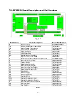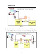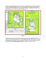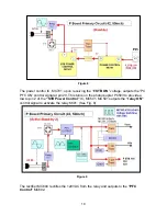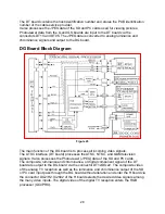
Upon receiving the power on command, pin 21 of IC4005 (Tuner Main ON) goes high
and pin 115 (Panel STB ON) goes low.
Pin 21 is connected to pin 28 of the connector PA20 via pin 1 of the connector DG20.
The high at pin 21 is the control signal used to turn on the circuit that generates the
SUB 3.3V, the Main 3.3V, the Main 5V, and the Main 9V sources of the PA board.
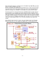
The low from pin 115 is connected to the base of Q4008 located on the DG board. It
causes Q4008 to stop conducting, and output a High to the base of Q9000 on the D
board, thus turning it on. When Q9000 is on, the collector goes low. This low is applied
to the gate of Q9003 turning it on to provide 5V to pins 1 and 2 of IC9008 (3.3V Reg.).
The 3.3V out of pin 4 of IC9008 is connected to the VCC pins 3, 24, 25, 28, 64, 89, and
100 of the microprocessor IC9003. The 3.3V is also connected to the reset circuit
IC9004.
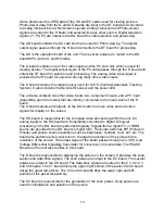
When IC9003 receives the 3.3V, it does a reset and outputs a high at pin 48 (Main
Panel ON). (See Fig. 12). This voltage is provided to pin 17 of the connector P25.
Figure 13
13
Summary of Contents for TH37PX50U - 37" HD PLASMA TV
Page 40: ...SC board Waveform Figure 30 SU And SD Board Shift Registers Figure 31 35 ...
Page 43: ...SS Board Schematic Figure 33 SS Board Waveform Figure 34 38 ...
Page 66: ...Adjustment Volume Locations Figure 53 61 ...
Page 67: ...Test Point Locations Figure 54 62 ...
Page 71: ...Scan and Sustain Drive Waveform Figure 55 Scan and Sustain Drive Check points Figure 56 66 ...

