


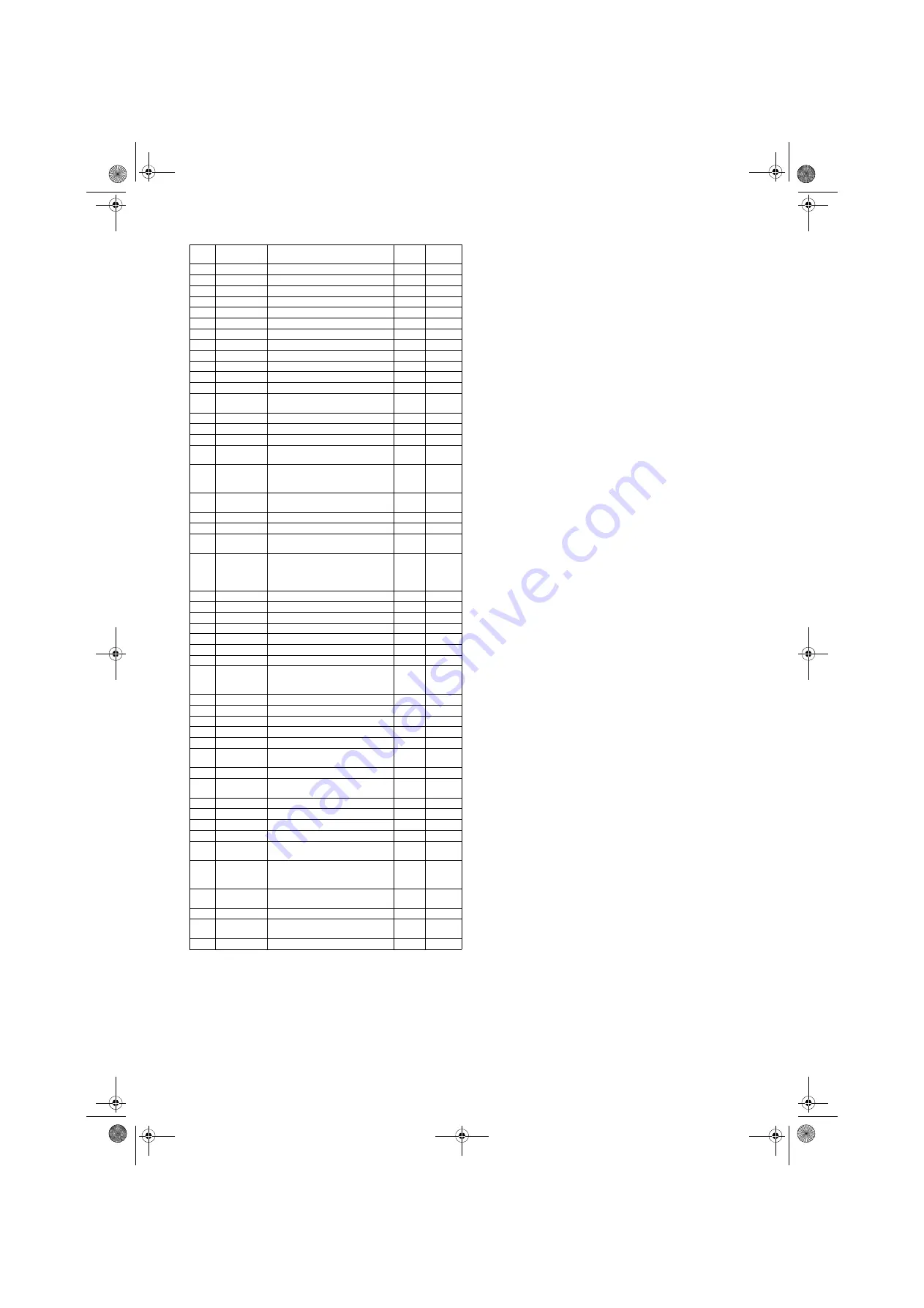
8
16
PIO[14]
Programmable input/output line.
O
0
17
PIO[8]
Programmable input/output line.
O
0
18
PIO[7]
Programmable input/output line.
O
0
19
PIO[6]
Programmable input/output line.
O
0
20
PIO[5]
Programmable input/output line.
O
0
21
PIO[4]
Programmable input/output line.
O
0
22
PCM_IN
Synchronous data input.
I
0
23
PCM_CLK
Synchronous data clock.
O
0
24
PCM_OUT
Synchronous data output.
O
0
25
PCM_SYNC
Synchronous data sync.
O
0
26
SPI_MOSI
SPI data input.
I
0
27
SPI_CLK
SPI clock.
I
0
28
SPI_CSB
Chip select for Serial Peripheral
Interface (SPI), active low.
I
2.88
29
SPI_MISO
SPI data output.
O
0
30
LED[0]
LED driver.
O
0
31
LED[1]
LED driver.
O
0
32
VREGIN_H
Input to internal high-voltage linear
regulator. (2.5V-4.9V)
I
3.05
33
VREGEN_H
Take high to enable high-voltage
linear regulator and switch-mode
regulator.
I
3.05
34
VREGOUT_H High-voltage linear regulator output.
(1.8V out)
O
1.84
35
N.C.
Not connection.
O
0
36
GND
Digital Ground.
GND
0
37
VDD_CHG
Lithium ion/polymer battery charger
input. (4.5V-6.5V)
I
0
38
VDD_BAT
Lithium ion/polymer battery positive
terminal.Battery charger output and
input to switch-mode regulator.
(4.2V out)
O
0
39
GND
Digital Ground.
GND
0
40
MIC_BIAS
Microphone bias.
I
0
41
MIC_R_P
Microphone input positive,right.
I
0
42
MIC_R_N
Microphine input negative,right.
I
0
43
MIC_L_P
Microphone input positive,left.
I
0
44
MIC_L_N
Microphone input negative,left.
I
0
45
AGND
Analogue Ground.
GND
0
46
VDD_AUDIO
Positive supply output for audio
circuitry and 1.5V regulated output.
(from internal low-voltage regulator)
O
1.51
47
SPK_R_N
Speaker output negative,right.
O
0
48
SPK_R_P
Speaker output positive,right.
O
0
49
SPK_L_N
Speaker output negative,left.
O
0.71
50
SPK_L_P
Speaker output positive,left.
O
0.71
51
PIO[3]
Programmable input/output line.
O
0
52
PIO[1]
Programmable input/output line.
(external TXEN)
O
0
53
PIO[2]
Programmable input/output line.
O
0
54
PIO[0]
Programmable input/output line.
(external RXEN)
O
0
55
GND
Digital Ground.
GND
0
56
GND
Digital Ground.
GND
0
57
ANT
RF out.
O
0
58
GND
Digital Ground.
GND
0
59
AIO[0]
Analogue programmable input/out
line.
O
0
60
VDD_ANA
Positive supply output for analogue
circuitry and 1.5V regulated output.
(from internal low-voltage regulator)
O
1.48
61
AIO[0]
Analogue programmable input/
output line.
O
0
62
GND
Digital Ground.
GND
0
63
USB_DP
USB data plus with selectable
internal 1.5k
Ω
pull-up resistor.
I
3.04
64
USB_DN
USB data minus.
I
0
Pin.
No.
PORT
Description
I/O
(V)
cqrxbt490u.book Page 8 Friday, April 6, 2012 9:48 AM
Summary of Contents for SiriusXM CQ-RXBT490U
Page 10: ...10 IC201 C1BA00000493 IC602 C3EBJY000032 cqrxbt490u book Page 10 Friday April 6 2012 9 48 AM ...
Page 11: ...11 IC400 C1BB00001088 cqrxbt490u book Page 11 Friday April 6 2012 9 48 AM ...
Page 12: ...12 IC50 C1ZBZ0004389 IC706 C0DBGYY00710 cqrxbt490u book Page 12 Friday April 6 2012 9 48 AM ...
Page 13: ...13 IC707 C0DBGYY00710 IC180 C0CBCYG00004 cqrxbt490u book Page 13 Friday April 6 2012 9 48 AM ...
Page 14: ...14 IC701 C0DAZYY00033 cqrxbt490u book Page 14 Friday April 6 2012 9 48 AM ...
Page 15: ...15 IC803 C1AB00003758 cqrxbt490u book Page 15 Friday April 6 2012 9 48 AM ...
Page 16: ...16 IC705 C0EBY0001290 cqrxbt490u book Page 16 Friday April 6 2012 9 48 AM ...
Page 17: ...17 IC902 B3RAB0000091 IC181 C0JBAB000255 cqrxbt490u book Page 17 Friday April 6 2012 9 48 AM ...
Page 50: ...50 2012 03 T cqrxbt490u book Page 50 Friday April 6 2012 9 48 AM ...


