


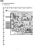


10 Schematic Diagram
10.1. Power Circuit
R501
4.7K
CN501
CN507
D502
D501
Q501
Q502
R546
1K
R504
15K
D501-D502
B0JAPG000019
E501
K4CZ01000027
Q520
B1GCCFJJ0016
INTERFACE SWITCH
IC501
R502
4.7K
R506
15K
R505
15K
R503
15K
FLin
IN GND
FRin
SUBin
Cin
-VD
+VD
SRin
SLin
RELA
Y
-Di SENS
+Di SENS
IH DET
DISP HMUT
SL_O
SR_O
GND
AC IN
C_O
-VCC LOW
+VCC LOW
SUB_O
-VCC HI
+VCC HI
FR_O
FL_O
C501
1000P
C503
1000P
C506 1000P
C505 1000P
R513
56K
C507 18P
C508 18P
R514 56K
R516 56K
C510 22P
R515 56K
C509 22P
R517 56K
C511 22P
R518 56K
C512 22P
R509
4.7K
R510 4.7K
R507
3.9K
R511
15K
R512
15K
R508 3.9K
C516
0.01
C515
0.01
C517
0.01
R402
1K
Q503
R532
4.7K
R523 20K
R524
120K
R526
120K
R527
120K
C513
0.047
R519
820K
R530 1
R531 1
R521 10K
R522 27K
R545
220K
Q506
B1GCCFJJ0016
INTERFACE SWITCH
Q505
B1AACF000117
SWITCHING
Q501-Q502
B1AACF000117
SWITCH
Q503
B1AACF000117
SWITCH
IC501
RSN311W64D-P
POWER HIC
C551
0.01
+
-
R525
150K
D558,D559
B0AACK000004
D555
B0AACK000004
D562
B0AACK000004
25
24
23
22
21
20
19
18
17
16
15
14
13
12
11
10
2
4
6
8
9
7
5
3
1
1
2
: +B SIGNAL LINE
: MAIN SIGNAL LINE
: -B SIGNAL LINE
TO FAN
TO
MAIN CIRCUIT
(JK2000) OF
SA-HT840EE-S
R583
100
R584
47K
D559
D558
R582
220K
C576
50V 10P
C577
16V 10
R603
10K
C647
6.3V 470
D560
B0AACK000004
R606 22
D557
B0EAKM0001
17
C575
0.01
Q555
Q555
2SD0592ARA
FAN MOTOR DRIVE
Q556
B1ACCF000094
FAN MOTOR DRIVE
Q554
B1ACCF000094
FAN MOTOR DRIVE
Q554
C574
0.01
D556
B0BA01100004
C570
25V 330
R564
220K
R563
1K
R602
4.7K
Q552
B1ACCF000094
FAN MOTOR DRIVE
Q553
2SD0592ARA
FAN MOTOR DRIVE
Q552
R559
10K
R558
100K
C578
0.01
C579
0.01
R604
2.2M
R562
4.7K
R581
6.8K
Q553
Q557
C580
50V 2.2
R529 22K
Q556
R520 22K
C514 6.3V100
R528 150K
D508
B0AACK000004
26
25
24
23
22
21
20 19
18
17
16
15
14 13
12
11
10
9
8
7
6
5
4
3
2
1
Q557
2SD0592ARA
FAN MOTOR DRIVE
C504 1000P
C502 000P
SCHEMATIC DIAGRAM-1
POWER CIRCUIT
AC1
DC_DET
AC2
SYS6V
HP_CNT
D.GND
FL
SUB+B
A.GND
A.GND
FR
SL
A.GND
SR
C
A.GND
SW
A.GND
PCONT
SYNC
FL
AC2
FL
AC1
Fan Control
D503
D503
MA2C700A0F
D504
B0AACK000004
C529 0.1
R549 3.9K
R547
390K
C534
50V33
R548
330K
17
SB-WA840EE