background image

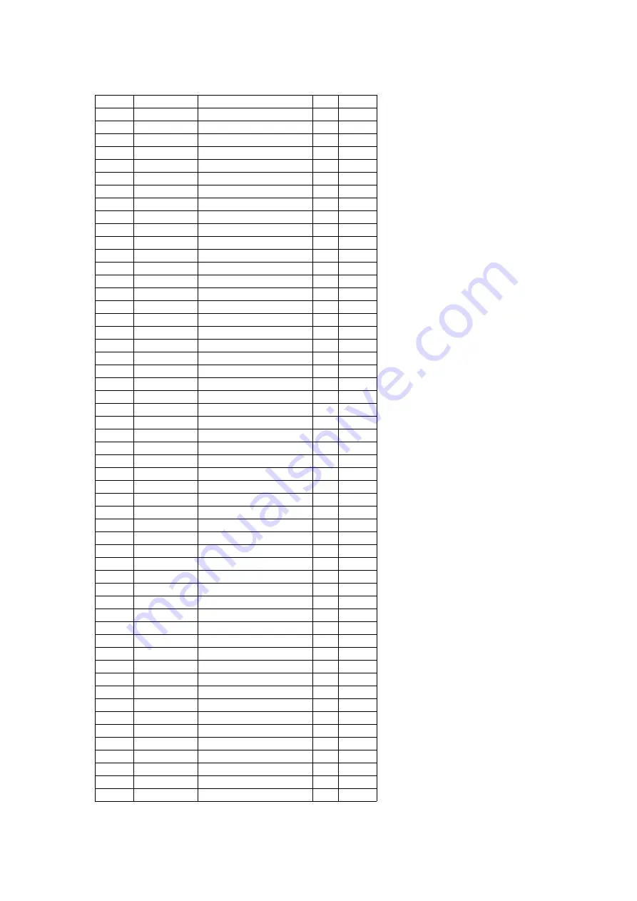
Ref. No.

Part No.

Part Name & Description

Pcs. Remarks

C134

ECUV1H270JCN 27P 50V

1 [M]

C136

ECUV1H102KBN 1000P 50V

1 [M]

C137

ECUV1H332KBN 3300P 50V

1 [M]

C138

ECUV1H103KBN 0.01 50V

1 [M]

C139

ECEA1EKA4R7B 4.7 25V

1 [M]

C141

ECEA1HKA010B 1 50V

1 [M]

C142

ECEA1HKA010B 1 50V

1 [M]

C143

ECUV1H682KBN 6800P 50V

1 [M]

C144

ECUV1H682KBN 6800P 50V

1 [M]

C147

ECUV1H102KBN 1000P 50V

1 [M]

C148

ECUV1H103KBN 0.01 50V

1 [M]

C149

ECUV1E104ZFN

0.1 25V

1 [M]

C201

ECUZ1H101JCN

100P 50V

1 [M]

C202

ECUZ1H101JCN

100P 50V

1 [M]

C204

ECUV1H221KBN 220P 50V

1 [M]

C207

ECEA1HKA010B 1 50V

1 [M]

C208

ECUZ1E563KBN 0.056 25V

1 [M]

C209

ECEA1HKAR15B 0.15 50V

1 [M]

C210

ECUZ1E223KBN 0.022 25V

1 [M]

C211

ECUZNC393KBN 0.039 16V

1 [M]

C212

ECUZ1E223KBN 0.022 25V

1 [M]

C213

ECUZ1H332KBN 3300P 50V

1 [M]

C214

ECUZ1H222KBN 2200P 50V

1 [M]

C215

ECUZ1H272KBN 2700P 50V

1 [M]

C216

ECUZ1H152KBN 1500P 50V

1 [M]

C217

ECUZ1C333KBN 0.033 16V

1 [M]

C218

ECEA1HKAR15B 0.15 50V

1 [M]

C219

ECEA1HKAR15B 0.15 50V

1 [M]

C220

ECUZ1H102KBN 1000P 50V

1 [M]

C221

ECUZNC683KBN 0.068 16V

1 [M]

C222

ECUZ1H471KBN 470P 50V

1 [M]

C223

ECEA1CKA100B 10 16V

1 [M]

C224

ECEA1HKA3R3B 3.3 50V

1 [M]

C225

ECEA1HKA3R3B 3.3 50V

1 [M]

C226

ECUZ1E104MBN 0.1 25V

1 [M]

C227

ECUV1H681KBV 680P 50V

1 [M]

C228

ECEA1CKA100B 10 16V

1 [M]

C229

ECUZ1H101JCN

100P 50V

1 [M]

C230

ECUZ1H470JCN

47P 50V

1 [M]

C232

ECUV1H332KBN 3300P 50V

1 [M]

C233

ECEA1CKA100B 10 16V

1 [M]

C234

ECUZNC683KBN 0.068 16V

1 [M]

C235

ECUZ1E183KBN 0.018 25V

1 [M]

C236

ECUZ1C474ZFN

0.47 16V

1 [M]

C237

ECUZ1H102KBN 1000P 50V

1 [M]

C240

ECEA1HKA010B 1 50V

1 [M]

C241

ECUZ1H101JCN

100P 50V

1 [M]

C242

ECEA1HKA3R3B 3.3 50V

1 [M]

C300

ECUZ1C103KBN 0.01 16V

1 [M]

C301

ECUZ1H102KBN 1000P 50V

1 [M]

C304

ECEA1AM331B

330 10V

1 [M]

C305

ECUZ1H152KBN 1500P 50V

1 [M]

C306

ECEA1HKA0R1B 0.1 50V

1 [M]

C307

ECUZ1H102KBN 1000P 50V

1 [M]

98

Summary of Contents for SAAK58 - MINI HES W/CD

Page 1: ...ER No MD0005087C3 CD Stereo System SA AK58 Colour S Silver Type Areas GN Oceania TAPE SECTION AR2 MECHANISM SERIES CD SECTION RAE0152Z M TRAVERSE DECK SERIES SYSTEM SC AK58 SPECIFICATIONS Specifications 1 ...

Page 2: ...equency range 87 5 108 00MHz 50kHz steps Sensitivity 2 5 V IHF S N 26dB 2 2 V Antenna terminal s 75 unbalanced AM TUNER SECTION Frequency range 522 1629kHz 9kHz steps Sensitivity S N 20dB 560 V m CASSETTE DECK SECTION Track system 4 track 2 channel Heads Record playback Soild permalloy head Erasure Double gap ferrite head Motor DC servo motor Recording system AC bias 100kHz Erasing system AC erase...

Page 3: ... 25W Eco mode off 18W Notes 1 Specifications are subject to change without notice Weight and dimensions are approximate 2 Total harmonic distortion is measured by the digital spectrum analyzer 1 Manufactured under license from Dolby Laboratories Locensing Corporation Dolby the double D symbol and PRO LOGIC are trade marks of Dolby Laboratories Licensing Corporation SYSTEM SC AK58 Main unit SA AK58...

Page 4: ... Circuitry The protection circuitry may have operated if either of the following conditions are noticed No sound is heard when the power is switched ON Sound stops during a performance The function of this circuitry is to prevent circuitry damage if for example the positive and negative speaker connection wires are shorted or if speaker systems with an impedance less than the indicated rated imped...

Page 5: ...icity damage to the laser diode use a short pin or similar tool to short the optical pickup s flexible circuit boards after they have been disconnected from the main circuit board 3 Handle the flexible circuit boards with care excessive force could cause them to be broken 4 Do not turn the pre set variable resistor for adjustment of the laser power it has been adjusted at the factory as shown in F...

Page 6: ...verse Deck The traverse deck has a short point shorted with solder protect the laser diode against electrostatic breakbown Be sure to remove the solder from the short point before making connections CAUTION THIS PRODUCT UNTILIZES A LASER USE OF CONTROLS OR ADJUSTMENTS OR PERFORMANCE OF PROCEDURES OTHER THAN THOSE SPECIFIED HEREIN MAY RESULT IN HAZARDOUS RADIATION EXPOSURE 5 Precaution of Laser Dio...

Page 7: ...6 Location of Controls 7 ...

Page 8: ...7 Location of Controls for Remote Control Transmitter 8 ...

Page 9: ... describes procedures for checking the operation of the major printed circuit boards and replacing the main components For reassembly after operation checks or replacement reverse the respective procedures Special reassembly procedures are described only when required 9 ...

Page 10: ...8 1 Checking for the main P C B 10 ...

Page 11: ... B as shown below 8 2 Disassembly for the CD changer ass y The CD changer unit can be removed until the tray base ornament would removed 8 2 1 Disassembly for the disc tray ornament Follow the Step 1 Step 3 of item 8 1 11 ...

Page 12: ...12 ...

Page 13: ...13 ...

Page 14: ...8 2 2 Disassembly for the CD changer unit Follow the Step 1 Step 3 of item 8 1 Follow the disassembly instruction for the disc tray ornament of item 8 2 1 14 ...

Page 15: ...orizontally when loading the CD changer unit 8 3 1 Initial setting of CD unit Follow the Step 1 Step 3 of item 8 1 Follow the disassembly instruction for the disc tray ornament of item 8 2 1 Follow the disassembly instruction for the CD changer unit of item 8 2 2 15 ...

Page 16: ...8 3 2 Checking for the CD servo P C B The initial setting of CD unit must be completed Refer to the initial setting of CD unit in item 8 3 1 16 ...

Page 17: ...vo P C B as shown below 8 3 3 Checking for the dolby prologic P C B FL P C B and cassette mechanism control P C B The initial setting of CD unit must be completed Refer to the initial setting of CD unit in item 8 3 1 17 ...

Page 18: ...loogic P C B FL P C B and cassette mechanism control P C B as shown below 8 3 4 Checking for the power supply P C B The initial setting of CD unit must be completed Refer to the initial setting of CD unit in item 8 3 1 18 ...

Page 19: ... Check the power supply P C B as shown below 8 4 Replacement for the traverse deck ass y Follow the Step 1 Step 3 of item 8 1 19 ...

Page 20: ... Follow the disassembly instruction for the disc tray ornament of item 8 2 1 Follow the disassembly instruction for the CD changer unit of item 8 2 2 20 ...

Page 21: ...21 ...

Page 22: ...22 ...

Page 23: ...23 ...

Page 24: ...eplacement for the disc tray Follow the Step 1 Step 3 of item 8 1 Follow the disassembly instruction for the disc tray ornament of item 8 2 1 Follow the disassembly instruction for the CD changer unit of 24 ...

Page 25: ...item 8 2 2 25 ...

Page 26: ...26 ...

Page 27: ...27 ...

Page 28: ...ollow the Step 1 Step 11 of item 8 1 Follow the disassembly instruction for the disc tray ornament of item 8 2 1 Follow the disassembly instruction for the CD changer unit of item 8 2 2 Follow the Step 1 Step 9 of item 8 4 Follow the Step 1 Step 11 of item 8 5 28 ...

Page 29: ...29 ...

Page 30: ...30 ...

Page 31: ...31 ...

Page 32: ...32 ...

Page 33: ...33 ...

Page 34: ...34 ...

Page 35: ...35 ...

Page 36: ...36 ...

Page 37: ...37 ...

Page 38: ...ass y Follow the Step 1 Step 3 of item 8 1 Follow the disassembly instruction for the disc tray ornament of item 8 2 1 Follow the disassembly instruction for the CD changer unit of item 8 2 2 Follow the Step 1 Step 10 of item 8 5 38 ...

Page 39: ...39 ...

Page 40: ... and head block Follow the Step 1 Step 3 of item 8 1 Follow the disassembly instruction for the disc tray ornament of item 8 2 1 Follow the disassembly instruction for the CD changer unit of item 8 2 2 Follow the Step 1 Step 3 of item 8 3 3 40 ...

Page 41: ...41 ...

Page 42: ...nding belt Follow the Step 1 Step 3 of item 8 1 Follow the disassembly instruction for the disc tray ornament of item 8 2 1 Follow the disassembly instruction for the CD changer unit of item 8 2 2 Follow the Step 1 Step 3 of item 8 3 3 Follow the Step 1 Step 11 of item 8 8 42 ...

Page 43: ...43 ...

Page 44: ...44 ...

Page 45: ...45 ...

Page 46: ...llow the disassembly instruction for the disc tray ornament of item 8 2 1 Follow the disassembly instruction for the CD changer unit of item 8 2 2 Follow the Step 1 Step 5 of item 8 3 3 Follow the Step 1 Step 6 of item 8 8 8 11 Replacement for the cassette lid ass y Follow the Step 1 Step 3 of item 8 1 46 ...

Page 47: ...8 12 Measure for tape trouble Follow the Step 1 Step 3 of item 8 1 47 ...

Page 48: ...mechanism controller or governor circuit 9 1 Operation Check Providing with Cassette Tape 1 Push up the EJECT lever with rubber band Refer to Fig 2 2 Apply DC 5V to the MOTOR MOTOR will be rotated Refer to Fig 1 3 Provide the cassette tape with mechanism ass y 4 Apply DC 9V to the plunger and then operate it by switching 48 ...

Page 49: ... D REV PLAY At STOP mode supply power to the plunger for ordinary duration Duration approx 200msec E REV REW At REV PLAY mode supply power to the plunger momentary Duration approx 50msec F STOP At REV REW mode supply power to the plunger momentary Duration approx 50msec Repeat the above operation to FWD PLAY mode Note Incorrect duration for power supply may be operated to other mode 9 1 1 Connecti...

Page 50: ...9 1 2 Detail View of EJECT Lever EJECT lever fixed by rubber band Plunger rib operation Fig 2 50 ...

Page 51: ...e it same as power supply duration Refer to Fig 3 Note Operation order is same as the Operation Check Providing with Cassette Tape item 4 above Fig 3 10 Self Diagnostic Display Function Self Diagnostic display This unit is equipped with a self diagnostic display function which if a problem occurs will display an error code corresponding to the problem Use this function when performing maintenance ...

Page 52: ... Press MEMORY button FAST FORWARD shall be executed for 2 seconds afterwhich it will STOP 4 Load a cassette tape with the erasure prevention tab removed from the right side only and close the cassette holder 5 Press FM MODE BP button REWIND shall be executed for 2 seconds afterwhich it will STOP 6 Load a pre recorded tape with both recording tabs intact and close the cassette holder 7 Press TUNE T...

Page 53: ...ck H02 because of no recording function CD Mechanism Test F15 F16 F17 F26 F27 F28 F29 H15 1 Press CD button 2 Press CD Manager button 3 Press TUNE MODE button to indicate Error Code To clear all Error Code 1 Press TUNE MODE button 2 FL will display CLEAR for 1 second and changer to T How to cancel Self Diagnostic Function 1 Press POWER button OFF Power Amplifier Failure F61 1 When power amplifier ...

Page 54: ...n the specified time about 8 seconds 2 CD tray opens automatically F16 CLAMP switch S4 NG Check Replace 3 Does not startup when TUNE TIME ADJ button is pressed F17 BOTTOM switch S5 NG Check Replace 4 Transmission error between CD servo LSI and micon F26 CD does not function This error occurs when the POWER is ON for the CD block and an error is detected after the transmission has started 5 Startup...

Page 55: ...operate CD PLAY with CD unit being connected only and CD Automatic Alignment result is shown on FL display How to set CD test mode CD Automatic Alignment result indication Under CD test mode pressing the numeric key 0 on the remote controller will display the auto adjustment result FLOCK TLOCK and CLVS status shall be shown as bellow 55 ...

Page 56: ...e coil 100 H AM loop antenna Note Trimmer will be instability that once you tighten please adjust with tighten slowly from loosened condition Adjust OSC coil and IFT with nonmetal driver 13 1 2 AM IF Adjustment 1 Connect the instrument as shown in Fig 1 2 Set the unit to AM mode 3 Apply signal sa shown in Fig 1 from AM SG 4 Adjust Z102 so that the output frequency is maximized in Fig 2 Fig 1 Fig 2...

Page 57: ...eive 520kHz in the unit 5 Adjust Z101 OSC so that the EVM AC is maximized 6 Set AM SG to 603kHz 7 Receive 603kHz in the unit 8 Adjust Z101 ANT so that the EVM AC is maximized 9 Set AM SG to 520kHz 10 Receive 520kHz in the unit 11 Adjust Z101 OSC so that the EVM DC value is within 0 5 1 1V Fig 3 13 1 4 Adjustment point 57 ...

Page 58: ...the screws and springs a fine adjustment cannot be done because of the screw locking bond adhered to the azimuth screw and spring Please remove the screw locking bond left on the head base when replacing the azimuth screw If you wish to readjust the head azimuth be sure to adjust with adhering the cassette tape closely to the mechanism by pushing the center of cassette tape with your finger shown ...

Page 59: ...the level difference forward and reverse directions 4 Playback the playback gain adjustment portion 315Hz 0dB of test tape QZZCFM Check if level difference between forward and reverse direction is within 1 5dB 5 After the adjustment apply screwlock to the azimuth adjusting screw Fig 5 Fig 6 Fig 7 59 ...

Page 60: ...he middle portion of it 2 Adjust motor VR Deck 2 for the output value shown below Adjustment target 2940 3060Hz NORMAL speed 3 After alignment assure that the output frequency of the DECK2 REV and DECK1 FWD are within 45Hz and 60Hz respectively of the value of the output frequency of DECK2 FWD Fig 9 Fig 10 60 ...

Page 61: ...ithin the standard value Standard value 98 8kHz Fig 11 13 2 5 Bias Voltage Check 1 Set the unit to AUX position 2 Insert the Normal blank tape QZZCRA into DECK2 and set the unit to REC mode use REC STOP key 3 Measure and make sure that the output is within the standard value 4 Insert the CrO2 tape QZZCRX 5 Repeat step 2 and 3 Standard value Normal 19 4mV Standard value CrO2 27 5mV Fig 12 13 2 6 Er...

Page 62: ...the standard value 4 Insert the CrO2 tape QZZCRX 5 Repeat step 2 and 3 Standard value Normal more than 100mV Standard value CrO2 more than 150mV Fig 13 13 2 7 Adjustment Point Fig 14 14 Illustration of ICs Transistors and Diodes 15 Schematic Diagram 15 1 Schematic Diagram Notes This schematic diagram may be modified at any time with the development of new technology Notes 62 ...

Page 63: ...rect play switch CD4 S608 Disc4 direct open close switch S609 Disc direct play switch CD5 S610 Disc5 direct open close switch S611 Dolby pro logic on off switch PRO LOGIC S612 Deck1 open switch DECK1 OPEN S613 Tape edit switch TAPE EDIT S614 Recording start stop switch REC STOP S615 Reverse mode select switch REV MODE S616 Disc2 open switch DECK2 OPEN S617 FF skip memory switch MEMORY S618 Playbac...

Page 64: ...h HALF S973 Deck2 CrO2 tape detect switch ATS CrO2 S974 Deck2 reverse side record prevention tab detect switch R REC INH S975 Deck2 forward side record prevention tab detect switch F REC INH VR600 Volume control VOLUME Indicated voltage values are the standard values for the unit meaured by the DC electronic circuit tester high impedance with the chassis taken as standard Therefore there may exist...

Page 65: ... are printed coils formed on the P C B and thus not found in the Replacement Parts list Voltage and signal line Positive voltage line Negative voltage line CD signal line FM signal line FM OSC signal line AM signal line AM OSC signal line Tape playback signal line Tape recording signal line Center SP drive signal line Surround SP drive signal line 15 2 Schematic Diagram 16 Printed Circuit Board Di...

Page 66: ...ut 15 J JOG A B I Sound control signal input 16 CHG AD1 I Open detect switch S3 and clump detect switch S4 signal input 17 CHG AD2 I Position sensor D1 and bottom detect switch S5 signal input 18 SER2 O Serial data clock output for IC601 and IC1105 19 STATUS I Status signal input from CD circuit 20 SQCLK O CD subcode clock output 21 SD I Station detector signal input for tuner circuit 22 SUBQ I CD...

Page 67: ...I Oscillator connection Sub clock 32 768kHz 37 XCOUT O Oscillator connection Sub clock 32 768kHz 38 XIN I Oscillator connection Main clock 8 0kHz 39 XOUT O Oscillator connection Main clock 8 0kHz 40 VSS GND 41 MBP1 O Beat proof control signal output 42 MBP2 O Beat proof control signal output 43 CHG SW2 I Disc tray position 2 detect signal input 44 CHG SW1 I Disc tray position 1 detect signal input...

Page 68: ...minal 2 F ch 3 Vcc I Power supply terminal 4 PDA I Focus signal input terminal 1 A ch 5 PDB I Focus signal input terminal 2 B ch 6 LPD I Laser PD signal 7 LD O Laser power auto control output 8 RF O RF amp terminal 9 RFIN I AGC input terminal 10 CSBRT I OFTR capacitor connection terminal 11 CEA I HPF AMP capacitor connection terminal 12 BDO O Dropout detection control 13 LDON I LD APC ON OFF H ON ...

Page 69: ... signal output Not used open 3 SRDATA Serial data signal output Not used open 4 DVDD1 I Power supply terminal 5 DVSS1 GND terminal 6 TX O Digital audio interface signal output 7 MCLK I Command clock signal input 8 MDATA I Command data signal input 9 MLD I Command load signal input 10 SENSE Sense signal Not used open 11 FLOCK Optical servo condition focus Not used open 12 TLOCK Optical servo condit...

Page 70: ...gnal output 28 FOD O Focus drive signal output 29 VREF I D A drive output normal voltage input 30 FBAL O Focus balance adj output 31 TBAL O Tracking balance adj output 32 FE I Focus error signal input 33 TE I Tracking error signal input 34 RFENV I RF envelope signal input 35 VDET I Oscillator detect signal input H detect 36 OFT I Off track signal input H Off track 37 TRCRS I Track cross signal inp...

Page 71: ...ot used open 56 SBCK Sub code serial input data Not used connected to GND 57 VSS GND terminal 58 X1 IN I Crystal oscillator terminal f 16 9344 MHz 59 X2 OUT O 60 VDD I Power supply terminal 61 BYTCK Byte clock signal Not used open 62 CLDCK Sub code frame clock signal Not used open 63 FCLK Crystal frame clock Not used open 64 IPFLAG Interpolation flag terminal Not used open 65 FLAG Flag terminal No...

Page 72: ...UBQ output mode select signal input Not used connected to VDD 20 4 IC703 AN8739SBE2 Focus Coil Tracking Coil Traverse Motor Spindle Motor Drive Pin No Terminal Name I O Function 1 RST Not used open 2 NC Not used 3 IN2 I Motor driver 2 input 4 PC2 I Turntable motor drive signal input L ON 5 NC Not used 6 IN1 I Motor driver 1 input 7 PVCC1 I Driver power supply terminal 1 8 PGND1 Driver GND terminal...

Page 73: ...ecial parts which have purposes of fire retardant resistors hight quality sound capacitors low noise resistors etc are used When replacing any of components be sure to use only manufactures specified parts shown in the parts list The ODSD mark in Remarks indicates source of supply The marking RTL indicates thet Retention Time is Limited for this item After the discontinuation of this assembly in p...

Page 74: ...MPER GEAR UNIT 2 M 24 RMB0474 CASS OPEN SPRING 2 M 25 RKW0603 V FL WINDOW 1 M 26 RUS757ZAA CASSETTE HALF SPRING 4 M 27 RGK1233 Q JOG ORNAMENT 1 1 M 28 RGK1240 Q JOG ORNAMENT 2 1 M 29 RGK1238B S JOG SHEET 1 M 30 RGU1848A Q FUNCTION BUTTON 1 M 31 RMKX0036 BOTTOM CHASSIS 1 M 32 RYQ0289 S JOY UNIT 1 M 33 RMKX0038A CD CHASSIS 1 M 34 SHE187 4 SPACER TRANS 2 M 35 RMN0203 PCB HOLDER 2 M 36 RGRX0016K C1 RE...

Page 75: ...0403 HEAB PANEL SPRING 2 M 113 RMB0404 BRAKE ROD SPRING 2 M 114 RMB0406 FR LEVER SP 2 M 115 RMB0408 THRUST SPRING 2 M 116 RML0370 TRIGGER LEVER 2 M 117 RML0371 FR LEVER 2 M 118 RML0372 WINDING LEVER 2 M 119 RML0374 EJECT LEVER 2 M 120 RMM0131 BRAKE ROD 2 M 121 RMM0133 1 EJECT ROD 2 M 122 RMQ0519 REEL HUB 4 M 123 RMS0398 1 MOVING CORE 2 M 124 RSJ0003 PLUNGER 2 M 125 RMC0061 PACK SPRING 2 M 126 RXF0...

Page 76: ...VER 1 M 319 RMM0201 SLIDE PLATE 1 1 M 320 RME0258 REAR LOCK SPRING 1 M 321 RML0521 REAR LOCK 1 M 322 RME0257 TRAY LOCK LEVER SPRI 1 M 323 RML0520 TRAY LOCK 1 M 324 RMM0202 SLIDE PLATE 2 1 M 325 XTB3 10J SCREW 11 M 326 RMR0334 FIXED PLATE 1 M 327 RMR0624 W2 CLAMPER 1 M 328 RMB0561 ASSIST LEVER SPRING 1 M 329 RMR1121 K MECHA COVER 1 M 330 RMA1110 2 TRAY ANGLE 1 M 331 RMR1122 H1 TRAY BASE 1 M 332 RMM...

Page 77: ... M 372 RMX0140 DISC SPACER 5 M 373 RME0261 FRONT LOCK SPRING 1 M 374 RMQ0742 SPINDLE BASE 1 M INTEGRATED CIRCUITS IC1 TA7291P IC DRIVE 1 M IC101 LA1833NMNTLM IC IF MPX 1 M IC102 LC72131MDTRM IC PLL 1 M IC301 M62456FPE1 IC BTL 1 M IC302 M5218AP IC BUFFER AMP 1 M IC303 M62433AFP IC AUDIO 1 M IC500 RSN311W64A P IC HIC 1 M IC501 STK470 040 IC HIC 1 M IC600 M38199MF229F IC MICRO PROCCESSOR 1 M IC601 BU...

Page 78: ...TRANSISTOR 1 M Q516 KTC3199GRTA TRANSISTOR 1 M Q519 2SB1417PQTA TRANSISTOR 1 M Q602 KTA12710YTA TRANSISTOR 1 M Q604 KRC103MTA TRANSISTOR 1 M Q605 2SA933SSTA TRANSISTOR 1 M Q606 KTC3199GRTA TRANSISTOR 1 M Q607 KRC102MTA TRANSISTOR 1 M Q608 KTC3199GRTA TRANSISTOR 1 M Q609 RVTDTC143EST TRANSISTOR 1 M Q610 RVTDTC143EST TRANSISTOR 1 M Q611 RVTDTC143EST TRANSISTOR 1 M Q701 2SA1037AKSTX TRANSISTOR 1 M Q8...

Page 79: ...R 1 M Q1220 DTA143XKA146 TRANSISTOR 1 M DIODES D1 GP1S94 DIODE 1 M D1A SVC211SPA AL DIODE 1 M D2 MTZJ4R7BTA DIODE 1 M D2A SVC211SPA AL DIODE 1 M D3 SVC211SPA AL DIODE 1 M D101 UDZSTE175R1B DIODE 1 M D201 1SS355TE17 DIODE 1 M D302 UDZSTE175R1B DIODE 1 M D306 DAP202KT146 DIODE 1 M D307 DAP202KT146 DIODE 1 M D308 1SS355TE17 DIODE 1 M D309 1SS355TE17 DIODE 1 M D311 1SS355TE17 DIODE 1 M D312 RL1N4003S ...

Page 80: ...D 1 M D611 SLR325MCT31W LED 1 M D612 SLR325MCT31W LED 1 M D613 SLR325MCT31W LED 1 M D614 MA723TA DIODE 1 M D615 1SS291TA DIODE 1 M D616 1SS291TA DIODE 1 M D617 RVD1SS133TA DIODE 1 M D625 RVD1SS133TA DIODE 1 M D627 RVD1SS133TA DIODE 1 M D628 RVD1SS133TA DIODE 1 M D629 RVD1SS133TA DIODE 1 M D630 RVD1SS133TA DIODE 1 M D631 RVD1SS133TA DIODE 1 M D632 RVD1SS133TA DIODE 1 M D633 RVD1SS133TA DIODE 1 M D6...

Page 81: ...ISC 5 EJECT 1 M S611 EVQ21405R SW DOLBY PRO LOGIC 1 M S612 EVQ21405R SW DECK 1 OPEN 1 M S613 EVQ21405R SW TAPE EDIT 1 M S614 EVQ21405R SW REC STOP 1 M S615 EVQ21405R SW REV OPEN 1 M S616 EVQ21405R SW DECK 2 OPEN 1 M S617 EVQ21405R SW MEMORY 1 M S618 EVQ21405R SW TUNE UP 1 M S619 EVQ21405R SW TUNE MODE 1 M S620 EVQ21405R SW TUNE DOWN 1 M S621 EVQ21405R SW FM MODE 1 M S622 EVQ11G07K SW SOUND EQ DOWN...

Page 82: ...S638 EVQ21405R SW POWER 1 M 82 ...

Page 83: ...RJS1A5210 10P WIRE HOLDER 1 M CN309 RJS1A9414 1 14P CONNECTOR 1 M CN501 RJT119W13V 13P CONNECTOR 1 M CN502 RJP6G18ZA SOCKET 1 M CN600 RJT066H08F CONNECTOR 1 M CN701 RJS2A6016 16P FFC CONNECTOR 1 M CN702 RJS1A6719 1Q 19P FFC CONNECTOR 1 M CN801 RJU057G09 9P CONNECTOR 1 M CN802 RJU057G08 8P CONNECTOR 1 M CN1201 RJS8T7ZA 8P MOLEX 1 M CP304 RJT057G09 9P B B CONNECTOR 1 M CP305 RJT057G08 8P B B CONNECT...

Page 84: ... COMPONENT COMBINATIO Z101 RLA2Z007 T COIL 1 M Z102 RLI2Z021M T AM IF BLOCK 1 M Z501 ERZV10V511CS ZENER 1 M Z600 RCDRPM6937H4 REMOTE CTRL SENSOR 1 M Z971 EXBF7L355SYV RADA RESISTOR 1 M Z1101 EXBF7L355SYV RADA RESISTOR 1 M CERAMIC FILTERS CF201 RLFFETWND01M FM CF 1 M CF202 RLFFETWND01M FM CF 1 M RELAY RL501 RSY0037M C RELAY 1 M RL502 RSY0040M 0 PRIMARY RELAY 1 M OSCILLATORS X102 RLFDFT22DD DISCRIMI...

Page 85: ...K PIN 1 M JK600 RJJ37TK07 H JK HP 1 M EARTH TERMINAL E500 SNE1004 2 EARTH TERMINAL 1 M WIRES W1A REEX0089 PRIMARY WIRE YELLOW 1 M W1 REZ1023 1 4P WIRE 1 M W2A REEX0032 PRI WIRE BLACK 1 M W2 REZ1024 3P WIRE 1 M W500 REXX0202 2P TRANSFORMER WIRE 1 M W501 REXX0224 13P WIRE 1 M W601 RWJ1108080RR 8P WIRE 1 M W602 RWJ0208155RX 8P WIRE 1 M W603 REXX0223 6P WIRE 1 M W1100 RWJ8010160RX 10P WIRE 1 M W1200 R...

Page 86: ...A4 RSA0006 J FM ANTENNA 1 M 86 ...

Page 87: ...113 ERJ6GEYJ103V 10K 1 10W 1 M R114 ERJ6GEYJ562V 5 6K 1 10W 1 M R115 ERJ6GEYJ561V 560 1 10W 1 M R116 ERJ6GEYJ102V 1K 1 10W 1 M R117 ERJ6GEYJ473V 47K 1 10W 1 M R118 ERJ6GEYJ332V 3 3K 1 10W 1 M R119 ERJ6GEYJ472V 4 7K 1 10W 1 M R120 ERJ6GEYJ473V 47K 1 10W 1 M R121 ERJ6GEYJ223V 22K 1 10W 1 M R122 ERJ6GEYJ272V 2 7K 1 10W 1 M R123 ERJ6GEYJ683V 68K 1 10W 1 M R124 ERJ6GEYJ330V 33 1 10W 1 M R125 ERJ6GEYJ47...

Page 88: ... ERJ6GEYJ362V 3 6K 1 10W 1 M R226 ERJ6GEYJ101V 100 1 10W 1 M R230 ERJ6GEYJ473V 47K 1 10W 1 M R231 ERJ6GEYJ183V 18K 1 10W 1 M R232 ERJ6GEYJ392V 3 9K 1 10W 1 M R233 ERJ6GEYJ224V 220K 1 10W 1 M R234 ERJ6GEYJ222V 2 2K 1 10W 1 M R240 ERJ6GEYJ473V 47K 1 10W 1 M R248 ERJ6GEYJ390V 39 1 10W 1 M R249 ERJ6GEYJ390V 39 1 10W 1 M R300 ERJ6GEYJ472V 4 7K 1 10W 1 M R301 ERJ6GEYJ223V 22K 1 10W 1 M R302 ERJ6GEYJ183V...

Page 89: ...J6GEYJ473V 47K 1 10W 1 M R359 ERJ6GEYJ473V 47K 1 10W 1 M R371 ERJ6GEYJ222V 2 2K 1 10W 1 M R372 ERJ6GEYJ222V 2 2K 1 10W 1 M R401 ERJ6GEYJ103V 10K 1 10W 1 M R402 ERJ6GEYJ472V 4 7K 1 10W 1 M R407 ERJ6GEYJ562V 5 6K 1 10W 1 M R408 ERJ6GEYJ103V 10K 1 10W 1 M R409 ERJ6GEYJ473V 47K 1 10W 1 M R410 ERJ6GEYJ102V 1K 1 10W 1 M R411 ERJ6GEYJ222V 2 2K 1 10W 1 M R412 ERJ6GEYJ472V 4 7K 1 10W 1 M R413 ERJ6GEYJ393V ...

Page 90: ...DS2TJ272T 2 7K 1 4W 1 M R521 ERDS2TJ221T 220 1 4W 1 M R524 ERDS2TJ472T 4 7K 1 4W 1 M R527 ERDS2TJ152T 1 5K 1 4W 1 M R529 ERD2FCVJ4R7T 4 7 1 4W 1 M R532 ERDS2TJ563T 56K 1 4W 1 M R533 ERDS2TJ563T 56K 1 4W 1 M R534 ERDS2TJ563T 56K 1 4W 1 M R535 ERDS2TJ563T 56K 1 4W 1 M R536 ERDS2TJ563T 56K 1 4W 1 M R537 ERDS2TJ563T 56K 1 4W 1 M R546 ERDS2TJ474T 470K 1 4W 1 M R551 ERDS2TJ222T 2 2K 1 4W 1 M R552 ERDS1F...

Page 91: ...W 1 M R605 ERDS2TJ331T 330 1 4W 1 M R606 ERDS2TJ102T 1K 1 4W 1 M R607 ERDS2TJ102T 1K 1 4W 1 M R608 ERDS2TJ122T 1 2K 1 4W 1 M R609 ERDS2TJ182T 1 8K 1 4W 1 M R610 ERDS2TJ222T 2 2K 1 4W 1 M R611 ERDS2TJ272T 2 7K 1 4W 1 M R612 ERDS2TJ472T 4 7K 1 4W 1 M R613 ERDS2TJ682T 6 8K 1 4W 1 M R614 ERDS2TJ103T 10K 1 4W 1 M R615 ERDS2TJ223T 22K 1 4W 1 M R616 ERDS2TJ683T 68K 1 4W 1 M R617 ERDS2TJ102T 1K 1 4W 1 M R...

Page 92: ...677 ERDS2TJ102T 1K 1 4W 1 M R678 ERDS2TJ102T 1K 1 4W 1 M R680 ERDS2TJ152T 1 5K 1 4W 1 M R681 ERDS2TJ104T 100K 1 4W 1 M R682 ERDS2TJ104T 100K 1 4W 1 M R683 ERDS2TJ104T 100K 1 4W 1 M R684 ERDS2TJ104T 100K 1 4W 1 M R685 ERDS2TJ104T 100K 1 4W 1 M R686 ERDS2TJ104T 100K 1 4W 1 M R687 ERDS2TJ223T 22K 1 4W 1 M R688 ERDS2TJ102T 1K 1 4W 1 M R689 ERDS2TJ104T 100K 1 4W 1 M R691 ERDS2TJ223T 22K 1 4W 1 M R692 E...

Page 93: ... ERJ6GEYJ102V 1K 1 10W 1 M R805 ERJ6GEYJ563V 56K 1 10W 1 M R806 ERJ6GEYJ473V 47K 1 10W 1 M R807 ERJ6GEYJ561V 560 1 10W 1 M R808 ERJ6GEYJ221V 220 1 10W 1 M R822 ERJ6GEYJ102V 1K 1 10W 1 M R823 ERJ6GEYJ105V 1M 1 10W 1 M R826 ERJ6GEYJ222V 2 2K 1 10W 1 M R827 ERJ6GEYJ222V 2 2K 1 10W 1 M R835 ERJ6GEYJ183V 18K 1 10W 1 M R836 ERJ6GEYJ222V 2 2K 1 10W 1 M R843 ERJ6GEYJ102V 1K 1 10W 1 M R844 ERJ6GEYJ102V 1K ...

Page 94: ...W 1 M R918 ERDS2TJ224T 220K 1 4W 1 M R919 ERDS2TJ103T 10K 1 4W 1 M R920 ERDS2TJ101T 100 1 4W 1 M R923 ERDS2TJ101T 100 1 4W 1 M R926 ERDS2TJ473T 47K 1 4W 1 M R929 ERDS2TJ104T 100K 1 4W 1 M R932 ERDS2TJ104T 100K 1 4W 1 M R935 ERDS2TJ104T 100K 1 4W 1 M R938 ERDS2TJ680T 68 1 4W 1 M R939 ERDS2TJ681T 680 1 4W 1 M R940 ERDS2TJ106T 10M 1 4W 1 M R941 ERDS2TJ101T 100 1 4W 1 M R942 ERDS2TJ680T 68 1 4W 1 M R9...

Page 95: ...03T 10K 1 4W 1 M R981 ERDS1FVJ180T 18 1 2W 1 M R981 ERDS2TJ103T 10K 1 4W 1 M R982 ERDS2TJ562T 5 6K 1 4W 1 M R983 ERDS2TJ222T 2 2K 1 4W 1 M R983A ERDS2TJ562T 5 6K 1 4W 1 M R984 ERDS2TJ151T 150 1 4W 1 M R984A ERDS2TJ562T 5 6K 1 4W 1 M R985 ERDS1FVJ220T 22 1 2W 1 M R1101 ERJ6GEYJ334A 330K 1 10W 1 M R1102 ERJ6GEYJ104A 100K 1 10W 1 M R1103 ERJ6GEYJ153A 15K 1 10W 1 M R1104 ERJ6GEYJ153A 15K 1 10W 1 M R11...

Page 96: ...RJ6GEYJ470A 47 1 10W 1 M R1170 ERJ6GEYJ102A 1K 1 10W 1 M R1172 ERJ6GEYJ331A 330 1 10W 1 M R1173 ERJ6GEYJ103A 10K 1 10W 1 M R1174 ERJ6GEYJ103A 10K 1 10W 1 M R1176 ERJ6GEYJ472A 4 7K 1 10W 1 M R1177 ERJ6GEYJ562A 5 6K 1 10W 1 M R1178 ERJ6GEYJ1R2A 1 2 1 10W 1 M R1179 ERJ6GEYJ272A 2 7K 1 10W 1 M R1180 ERJ6GEYJ272A 2 7K 1 10W 1 M R1181 ERJ6GEYJ332A 3 3K 1 10W 1 M R1182 ERJ6GEYJ1R0A 1 1 10W 1 M R1183 ERJ6...

Page 97: ...ECEA1CKA100B 10 16V 1 M C103 ECUV1H103KBN 0 01 50V 1 M C104 ECUV1H102KBN 1000P 50V 1 M C106 ECUV1H103KBN 0 01 50V 1 M C107 ECUV1E473ZFN 0 047 25V 1 M C108 ECUV1H080DCN 8P 50V 1 M C109 ECUV1H102KBN 1000P 50V 1 M C110 ECUV1H103KBN 0 01 50V 1 M C111 ECEA1EKA4R7B 4 7 25V 1 M C112 ECUV1H103KBN 0 01 50V 1 M C113 ECUV1H102KBN 1000P 50V 1 M C114 ECEA1HKA3R3B 3 3 50V 1 M C115 ECEA1EKA4R7B 4 7 25V 1 M C116 ...

Page 98: ...M C215 ECUZ1H272KBN 2700P 50V 1 M C216 ECUZ1H152KBN 1500P 50V 1 M C217 ECUZ1C333KBN 0 033 16V 1 M C218 ECEA1HKAR15B 0 15 50V 1 M C219 ECEA1HKAR15B 0 15 50V 1 M C220 ECUZ1H102KBN 1000P 50V 1 M C221 ECUZNC683KBN 0 068 16V 1 M C222 ECUZ1H471KBN 470P 50V 1 M C223 ECEA1CKA100B 10 16V 1 M C224 ECEA1HKA3R3B 3 3 50V 1 M C225 ECEA1HKA3R3B 3 3 50V 1 M C226 ECUZ1E104MBN 0 1 25V 1 M C227 ECUV1H681KBV 680P 50V...

Page 99: ...4 ECEA1CKA100B 10 16V 1 M C401 ECUZ1H101JCN 100P 50V 1 M C402 ECUZ1H101JCN 100P 50V 1 M C404 ECUV1H221KBN 220P 50V 1 M C407 ECEA1HKA010B 1 50V 1 M C408 ECUZ1E563KBN 0 056 25V 1 M C409 ECEA1HKAR15B 0 15 50V 1 M C410 ECUZ1E223KBN 0 022 25V 1 M C411 ECUZNC393KBN 0 039 16V 1 M C412 ECUZ1E223KBN 0 022 25V 1 M C413 ECUV1H332KBN 3300P 50V 1 M C414 ECUZ1H222KBN 2200P 50V 1 M C415 ECUZ1H272KBN 2700P 50V 1 ...

Page 100: ...P 50V 1 M C529 ECBT1H150JC5 15P 50V 1 M C530 ECBT1H220JC5 22P 50V 1 M C531 ECBT1H220JC5 22P 50V 1 M C533 ECKR1H103ZF5 0 01 50V 1 M C534 ECEA1CKA470B 47 16V 1 M C539 ECBT1H473ZF5 0 047 50V 1 M C540 ECQV1H104JZ3 0 1 50V 1 M C543 ECEA1JM101B 100 63V 1 M C544 ECBT1H103KB5 0 01 50V 1 M C546 ECEA1AKA330B 33 10V 1 M C547 ECEA1CKA100B 10 16V 1 M C548 ECEA1HKA2R2B 2 2 50V 1 M C549 ECEA2AU100B 10 100V 1 M C...

Page 101: ...C622 ECEA0JKA101B 100 6 3V 1 M C623 ECBT1H102KB5 1000P 50V 1 M C624 RCEA0J102B S 1000 6 3V 1 M C625 ECBT1H102KB5 1000P 50V 1 M C627 ECBT1E103ZF5 0 01 25V 1 M C628 ECEA1AKA220B 22 10V 1 M C629 ECBT1H331KB5 330P 50V 1 M C630 ECBT1H561KB5 560P 50V 1 M C631 ECBT1H561KB5 560P 50V 1 M C632 ECBT1H561KB5 560P 50V 1 M C633 ECBT1H561KB5 560P 50V 1 M C634 ECBT1H101KB5 100P 50V 1 M C635 ECBT1H561KB5 560P 50V ...

Page 102: ...C704 ECUZ1E104MBN 0 1 25V 1 M C706 ECUZ1H272KBN 2700P 50V 1 M C707 ECUZ1E273KBN 0 027 25V 1 M C710 ECUZ1H121KCN 120P 50V 1 M C711 ECUZ1E104ZFN 0 1 25V 1 M C712 ECUZ1E104ZFN 0 1 25V 1 M C713 ECUZ1E104MBN 0 1 25V 1 M C714 ECEA0JKA101I 100 6 3V 1 M C715 ECUZ1H272KBN 2700P 50V 1 M C716 ECUZ1H821KBN 820P 50V 1 M C717 ECUZ1E104ZFN 0 1 25V 1 M C718 ECUZ1C224KBN 0 22 16V 1 M C721 ECUZ1H100DCN 10P 50V 1 M ...

Page 103: ...MR 0 082 16V 1 M C814 ECEA1HKAR47B 0 47 50V 1 M C815 ECEA1HKAR33B 0 33 50V 1 M C816 ECEA1CKA100B 10 16V 1 M C817 ECEA1HKA220B 22 50V 1 M C818 ECEA1CM221B 220 16V 1 M C819 ECUV1H330JCN 33P 50V 1 M C820 ECEA1HKA2R2B 2 2 50V 1 M C821 ECEA1CKA470B 47 16V 1 M C822 ECUZ1H101KBN 100P 50V 1 M C823 ECEA1HKA100B 10 50V 1 M C824 ECEA1CM221B 220 16V 1 M C825 ECFR1C183MR 0 018 16V 1 M C828 ECEA1HKA010B 1 50V 1...

Page 104: ... 0 01 500V 1 M C900 ECEA1CKA330B 33 16V 1 M C978 ECKR1H103ZF5 0 01 50V 1 M C980 ECKR1H103ZF5 0 01 50V 1 M C981 ECEA1EKA470B 47 25V 1 M C984 RCEA1C102B S 1000P 16V 1 M C1101 ECUZ1H102KBN 1000P 50V 1 M C1102 ECUZ1H102KBN 1000P 50V 1 M C1103 ECUZ1H681KBN 680P 50V 1 M C1104 ECFR1C223KR 0 022 16V 1 M C1105 ECUZ1H122KBN 1200P 50V 1 M C1106 ECUZ1H122KBN 1200P 50V 1 M C1108 ECEA1CKA330B 33 16V 1 M C1109 E...

Page 105: ...1 M C1153 ECUZ1H102KBN 1000P 50V 1 M C1154 ECUZ1H102KBN 1000P 50V 1 M C1162 ECEA1CKA101B 100 16V 1 M C1165 ECEA1CKA100B 10 16V 1 M C1166 ECEA1CKA100B 10 16V 1 M C1173 ECUZ1H103KBN 0 01 50V 1 M C1174 ECEA1HKA4R7B 4 7 50V 1 M C1175 ECEA1VU221B 220 35V 1 M C1176 ECQV1H473JZ3 0 047 50V 1 M C1177 ECUZ1H102KBN 1000P 50V 1 M C1178 ECUZ1H102KBN 1000P 50V 1 M C1179 ECUZ1H103KBN 0 01 50V 1 M C1180 ECUZ1H103...

Page 106: ... 1 10W 1 M RJ716 ERJ6GEY0R00A 0 1 10W 1 M RJ721 ERJ6GEY0R00A 0 1 10W 1 M RJ722 ERJ6GEY0R00A 0 1 10W 1 M RJ724 ERJ6GEY0R00A 0 1 10W 1 M RJ727 ERJ6GEY0R00A 0 1 10W 1 M RJ728 ERJ6GEY0R00A 0 1 10W 1 M RJ731 ERJ6GEY0R00A 0 1 10W 1 M RJ732 ERJ6GEY0R00A 0 1 10W 1 M RJ734 ERJ6GEY0R00A 0 1 10W 1 M RJ750 ERJ6GEY0R00A 0 1 10W 1 M TEST JUMPER TJ701 EYF8CU TEST JUMEPR 1 M 22 Cabinet Parts Location 106 ...

Page 107: ...107 ...

Page 108: ...23 Mechanism Parts Location 108 ...

Page 109: ...109 ...

Page 110: ...24 CD Mechanism Parts Location 110 ...

Page 111: ...25 Packaging 111 ...

Page 112: ...Printed in Japan M000500000MT 112 ...

Page 113: ... parts so the cut corner is located upper right Refer to the figure below 0N2180RLC 0N2180RLC1 Parts No Direction Remarks Note for IC971 replacement Two different types old or new parts are mounted on P C B as for IC971 When servicing care to replace the parts due to those shape Replacement procedures Old New Mount the parts on given position Printed pattern on P C B Mount the parts so the cut cor...

Page 114: ... S619 TUNE MODE S615 REV MODE S618 TUNE TIME ADJ S612 DECK 1 OPEN S621 FM MODE BP S617 MEMORY S616 DECK 2 OPEN 1 2 3 4 5 6 8 7 1 2 3 REPX0211A ELECTRICAL PARTS LOCATION OPERATION 2 P C B H Ref No Lo No Ref No Lo No OPERATION 1 P C B G D605 S611 S612 S613 S614 S615 S616 S617 S618 S619 S620 S621 S600A CP600 R617 D600 D601 D602 D603 D604 S600 S601 S602 S603 S604 S605 S606 S607 S608 S609 S610 H600 W60...

Page 115: ... C500 C502 R504 R586 C566 C501 C531 C513 POWER AMP P C B M REPX0319A SPEAKERS LOW 6 HIGH 6 L R CENTER SURROUND CENTER 8 SURROUND 8 ELECTRICAL PARTS LOCATION Ref No Lo No Ref No Lo No Ref No Lo No POWER AMP P C B M IC500 IC501 Q501 Q503 Q505 Q509 Q510 Q512 Q515 Q516 Q519 D501 D502 D503 D504 D506 D507 D508 D509 D512 D514 D516 D517 D518 D519 D520 D521 D522 D523 D524 D525 D526 D528 L501 RL500 RL501 CP...

Page 116: ...04 C887 C812 R802 R801 FC2 F1 JK500 T502 Z501 FC1 W1A W2A W500 ELECTRICAL PARTS LOCATION Ref No Lo No Ref No Lo No Ref No Lo No Ref No Lo No DPL P C B F AC IN P C B O IC801 IC802 IC803 IC804 Q801 Q802 Q803 Q804 D804 L801 X801 CN801 CN802 R801 R802 R803 R804 R805 R806 R807 R808 R822 R823 R826 R827 R835 R836 R843 R844 R847 R848 R855 R856 R857 R858 R859 R860 R863 R864 R865 R866 R867 R868 R871 R872 R8...

Page 117: ... CN1 1 2 3 4 W1 1 2 3 W2 Q1 E C B D2 J J J J C1 C2 S1 S2 RM1 LOADING MOTOR S3 R1 LOADING MOTOR P C B J PLUNGER REP2578A N ELECTRICAL PARTS LOCATION Ref No Lo No Ref No Lo No Ref No Lo No POWER TRANSFORMER P C B N LOADING MOTOR P C B J Q975 Q977 Q978 D513 D977 D978 D979 D980 D981 D982 D985 D986 T501 RL502 CN501 CN502 W1A W2A W500 R976 R978 R979 R980 R981 R983 R984 R985 R987 C540 C978 C980 C981 C984...

Page 118: ... R706 1K I H G F E D C C742 0 027 B A R701 4 7 C701 6 3V33 CN701 RF TP29 C716 820P TJ701 A B C D E D E C A B D C B A C751 0 1 C750 0 1 VREF C702 0 1 C706 2700P C707 0 027 C704 0 1 C703 6 3V100 Q701 2SA1037AKSTX LASER POWER DRIVE IC701 AN8839NSBE2 SERVO AMP IC703 AN8739SBE2 FOCUS COIL TRACKING COIL TRAVERSE MOTOR SPINDLE MOTOR DRIVE TRACKING COIL FOCUS COIL 0 1 2 12 11 3 8 10 5 4 9 680P 680P 1K 0 1...

Page 119: ...17 TP14 TP13 TP12 TP8 TP7 TP6 TP4 TP2 I H G F E D C B A S701 REST TP16 C745 1000P A B C D E F G H I G F E D C B A A B C D E F G H I R712 220 C718 0 22 C717 0 1 C744 8200P R709 68K R741 47K R711 82K C722 10P X701 16 9344MHz C721 10P C724 0 1 C723 10V220 IC702 MN662790RSC SERVO PROCESSOR DIGITAL SIGNAL PROCESSOR DIGITAL FILTER D A CONVERTER B 2 Rch OUT RST STAT SUBQ SQCK BLKCK P GND MDATA MCLK TX B ...

Page 120: ...X103 7 2MHz R117 47K C130 6 3V100 C132 1000P C113 1000P R132 10K R133 1K R130 10K R138 3 3K R137 1K R136 1K R135 1K R134 470 A B C D C125 16V22 R114 5 6K C110 0 01 A B C D E F IC102 LC72131MDTRM PLL FREQUENCY SYNTHESIZER AM ANT EXT LOOP FM ANT GND 75 JK101 B L2 0 47 H L1 1 2 H L102 1 H R151 82 MAIN TUNER CIRCUIT SCHEMATIC DIAGRAM 3 D3 SVC211SPA AL Q3 2SC2787FL1TA LOCAL OSC Q4 2SC2787FL1TA BUFFER A...

Page 121: ...1 22K C139 25V4 7 R102 4 7K C119 680P C116 0 033 R143 22K C115 25V4 7 R120 47K C109 1000P C114 50V3 3 R118 3 3K A D B C R104 1K C103 0 01 R107 330 C104 1000P R105 470 CF201 R106 470K 1 3 2 CF202 1 3 2 IC101 LA1833NMNTLM FM AM IF AMP DET AM OSC MIX FM MPX Q106 KRA102MTA POWER SUPPLY FM ON 7 3V 14 5V A B 11 10 9 8 7 6 5 4 3 2 1 GND 14 5V R126 1K R125 470 To MAIN CONTROL CIRCUIT on SCHEMATIC DIAGRAM ...

Page 122: ...1201 C1176 0 047 C1175 35V220 R1188 1K R1189 4 7K Q1171 2SD1302STA SWITCHING REC ON R1177 5 6K D1175 MA111TX C1182 50V4 7 Q1174 2SC2412KT96R BIAS OSC CONT CrO2 R1181 3 3K R1180 2 7K R1179 2 7K C1181 0 01 C1180 0 01 C1177 1000P C1179 0 01 C1178 1000P R1178 1 2 Q1175 1176 2SC2002KTA BIAS OSC Q1175 Q1176 TP5 TP4 TP2 TP1 R1184 100K C1102 1000P R1104 15K C1194 1000P R1195 100K C1103 680P C1104 0 022 R1...

Page 123: ...1122 33K R1146 10K R1121 33K C1143 50V4 7 C1127 0 01 R1117 270K R1115 390K C1131 820P C1129 820P R1123 10K R1125 1K C1146 16V10 C1135 1000P C1139 50V2 2 R1105 270 C1105 1200P C1108 16V33 C1109 16V100 C1111 820P C1113 6 3V220 R1107 39 C1115 0 033 R1141 6 8K R1109 4 3K R1111 2 2K C1147 1500P C1123 1800P C1119 50V4 7 C1121 50V1 C1125 0 047 C1136 1000P C1134 50V4 7 C1133 50V4 7 R1133 3 3K C1142 0 022 ...

Page 124: ...SWITCHING PLAY ON Q1151 Q1152 A G R1213 1 5K R1220 4 7K R1145 10K C1145 16V10 A B C D R1161 4 7K R1196 47K R1197 47K R1162 4 7K Q1115 Q1116 C1186 10V47 R1186 1K Q1115 1116 2SD2114K1V MUTING C1151 16V10 R1151 1M R1155 220 C1153 1000P Q1153 R1156 220 C1154 1000P R1152 1M C1152 16V10 R1154 1 2K R1153 1 2K C1166 16V10 C1165 16V10 C1162 16V100 R1158 220 A B C D Q1118 1119 2SC2412KT96R INTERFACE D1173 M...

Page 125: ... 10K B A D C VREF ADIN7 ADIN6 TPS VREF MK CLK MK DATA SW5V To FL CIRCUIT H602 on SCHEMATIC DIAGRAM 11 I 1 2 M MOTOR Q1203 2SD965RTA MOTOR DRIVE R1206 220 R1236 4 7K R1235 4 7K R1216 2 2K C1188 100P C1187 100P R1215 2 2K Q1208 DTC114TKA146 SOLENOID DRIVE D1202 MA111TX R1226 1K R1227 1K D1201 MA111TX R1225 2 7 R1221 2 7 Q1209 DTC114TKA146 SOLENOID DRIVE Q1206 2SB621RTA SOLENOID DRIVE Q1207 2SB621RTA...

Page 126: ... R RECT VCS TH VCS1 VCS2 VLR2 VLR1 VLR TH L RECT DC CUT R RECT DC CUT L BPF3 L BPF1 R IN L IN C TRIM DC CUT CMODE CAP A GND NS BPF1 NS BPF2 OSC1 CLK DATA ENABL DATA CLK ENABL2 DIGITAL GND OSC OSC V DD A D NS D A DC CUT DC CUT S OUT S VOL IN OP VREF S VOL OUT S OP IN S OP NF S OP OUT VOL REF C OP OUT C OP NF A GND C OP IN C VOL OUT Vcc NC NR 1REF R MIX OUT L BPF2 R847 4 7K R855 6 8K R874 100K R848 ...

Page 127: ...25 CLOCK TIMER R666 1 2K S634 RANDOM R659 1 8K S632 DISPLAY DEMO R656 2 2K S630 S WOOFER R652 2 7K S626 R642 4 7K S624 R648 2 7K S623 S622 R654 4 7K S628 3D AI EQ R695 330 D609 SLR325MCT31W S WOOFER R697 330 D610 SLR325MCT31W AUX R900 330 D611 SLR325MCT31W TAPE R903 330 D612 SLR325MCT31W TUNER R909 330 D613 SLR325MCT31W CD A C E D B JK600 PHONES L602 100 H L603 100 H L604 10 H C605 0 022 C606 0 02...

Page 128: ... R958 4 7K R955 470K D630 RVD1SS133TA 3 2 1 VDD GND OUT Z600 RCDRPM6937H4 REMOTE SENSOR R693 47 C621 25V4 7 C620 0 01 R964 22K D632 RVD1SS133TA D631 RVD1SS133TA R627 100 B A C D E R633 1K C604 100P C603 100P IC601 BU2090AF E2 LED DRIVE C602 0 1 8 9 7 10 6 11 5 12 4 13 3 2 1 14 15 16 MUTE A CLK LEDCTL REC PLAY D5 D4 D3 D2 D1 Vcc DATA GND CD PCONT R691 22K R694 4 7K R650 4 7K R661 390 D608 SLR325DCT...

Page 129: ...P Q608 C669 1000P R959 4 7K C668 1000P Q606 C665 56P C660 68P C666 56P X600 32 7kHz C657 18P C655 15P R943 330K R940 10M R948 1K R974 10K i j D A B Q604 KRC103MTA RESET R957 22K R960 470 C658 100P C667 50V2 2 D629 RVD1SS133TA R967 22K R926 47K C649 0 01 C656 100P C662 50V1 D616 1SS291TA D615 1SS291TA I G H V U S W T L605 3 3 H D614 MA723TA R910 680 C624 6 3V1000 C623 1000P C622 6 3V100 C625 1000P ...

Page 130: ...V0 1 R929 100K C650 50V0 1 C647 50V0 1 C653 0 01 C646 0 01 a Z X Y FL600 RSL0296 F 1 2 6 7 8 9 10 11 12 13 14 15 16 17 18 19 20 21 22 23 24 25 26 27 28 29 30 31 32 33 34 35 36 37 38 39 40 41 42 43 46 47 FL DISPLAY 3 44 45 48 49 51 52 53 5 C616 35V22 C661 50V3 3 R938 68 R942 68 D638 MA4020LTA A B C D E F G H I J K L M N O P Q R S T U V A B C D E F G H I J K L M N O P Q R S T W U C648 35V22 A B C R6...

Page 131: ...OR CIRCUIT 14 2 1 3 4 5 6 7 8 9 10 11 12 13 CN1 PLUNGER S2 TRAY POSITION2 DET S1 TRAY POSITION1 DET S3 OPEN DET IC1 TA7291P MOTOR DRIVE A B C D 8 7V M 1 2 3 4 5 6 7 8 9 10 R1 1K C1 16V100 D2 MTZJ4R7BTA Q1 RVTDTC143EST MOTOR DRIVE RM1 LOADING MOTOR C2 0 01 J K L SCHEMATIC DIAGRAM 14 POSITIVE VOLTAGE LINE 7 7V 0V 0 6V 9 7V 0V 0V 9 8V 9 8V 0 6V ...

Page 132: ...1K D316 RL1N4003S P C236 0 47 R346 22K R345 220 14 2 1 3 4 5 6 7 8 9 10 11 12 13 CN309 R347 12K A B C R354 12K R355 22K D E F D312 RL1N4003S P R359 47K R351 10K R412 4 7K 2 1 3 4 5 6 7 8 10 9 2 1 3 4 5 6 7 8 R353 10K C401 100P C201 100P To FL CIRCUIT CP603 on SCHEMATIC DIAGRAM 13 To MECHANISM CONTROL CIRCUIT H1100 on SCHEMATIC DIAGRAM 8 C To MAIN TUNER CIRCUIT on SCHEMATIC DIAGRAM 4 B A B 14V B 7 ...

Page 133: ...PHONO AUX AVss AGND PHONO AUX EXT IN CD TAPE PB TUNER VIDEO MD DEL L ch R ch 33 GRAPHIC EQUALIZER GRAPHIC EQUALIZER R455 10K R456 4 7K R453 4 7K R452 10K C423 16V10 R418 3 3K R417 68K R416 2 2K C420 1000P C422 470P C421 0 068 C313 0 1 C316 150P C315 150P R324 2 2K R325 2 2K P Q R216 2 2K R217 68K R218 3 3K C220 1000P C222 470P C221 0 068 C223 16V10 D302 UDZSTE175R1B R322 270 R321 2 7 C312 0 1 R419...

Page 134: ...8 R432 3 9K R434 2 2K C440 50V1 C436 100P R444 22K R342 10K R334 270K R336 15K R337 8 2K C322 0 068 C321 10V33 R343 3 9K C323 0 047 C327 0 15 C328 0 068 C326 4700P R339 82K R340 82K 2 1 3 4 5 6 7 8 9 10 11 P GND D GND B 7 5V B 7 5V NC CD3 3V SW5V VP LED9V B 10V CN301 NC CD7 5V CN300 2 1 3 4 5 6 7 8 9 10 11 GND B 14V Lch OUT Rch OUT LOW OUT CD HP SW GND P CONT DC DET 12 12 A B A B D317 1SS355TE17 S...

Page 135: ...C531 22P D519 RK306LFU1 D517 RK306LFU1 R520 2 7K R513 4 7K R516 2 7K R512 2 7K R508 4 7K R509 2 7K 10 11 C548 50V2 2 R517 4 7K R568 22K R507 4 7K R561 10K C547 16V10 P GND B 10V LED9V 12 2 1 3 4 5 6 7 8 9 Lch IN CD B 14V 10 11 GND Rch IN LOW IN GND DC DET P CNT HP SW C CP501 D502 RL1N4003S P D503 RL1N4003S P C D Q510 2SD2144STA SWITCHING C554 10V470 C513 0 01 A B R554 1K S IN C IN E To MAIN CONTRO...

Page 136: ...6 1D3E C574 35V3300 D524 1D3E C571 35V3300 C573 5600 D521 1D3E C578 0 01 R594 3 3K R574 2 7K D528 RVD1SS133TA D522 MTZJ15CTA R577 2 2 D520 1D3E R572 2 2 Q519 2SB1417PQTA REGULATOR Q516 KTC3199GRTA STABILIZER C546 10V33 R569 3 9K R551 2 2K Q509 KRC110MTA SWITCHING Q512 2SC1740SSTA RELAY DRIVE C523 50V1 D509 MTZJ12BTA C572 5600 R593 820K C561 0 1 C562 0 1 R584 10 C565 0 1 C566 0 1 R586 10 C559 0 1 C...

Page 137: ...01 R983 2 2 D982 MTZJ6R8BTA R984 150 C980 0 01 C981 25V47 D981 1D3E R985 22 R981 18 R980 18 D978 1D3E Q977 2SC3940AQSTA REGULATOR T501 Q975 2SC1740SSTA RELAY DRIVE R978 1K W500 T502 F1 T2A W2A Z501 JK500 AC IN 230 240V 50Hz POWER TORANSFORMER CIRCUIT N SCHEMATIC DIAGRAM 20 AC IN CIRCUIT O D513 KBP202G C540 0 1 R979 RSFMB40KT L C984 1000 W1A D979 1D3E D985 1D3E D986 1D3E 16V 0 8V 0 2V 9 5V 6V 6 6V ...

Page 138: ...A E C B KRC102MTA KRC103MTA KRC110MTA KTC3199GRTA RVTDTC143EST 2SA1037AKSTX 2SC2412KT96R 2SD2114K1V DTA114EKA146 DTA143XKA146 DTC114TKA146 DTC144TKA146 E C B 2SC3940AQSTA E C B 1D3E RL1N4003S P A Ca Anode Cathode KRA102STA KRA111STA KRC102STA KRC111STA KTC3875GRTA KTD1304TA 2SK544F AC D G S MTZJ10BTA MTZJ12BTA MTZJ15CTA MTZJ16BTA MTZJ30BTA MTZJ4R7BTA MTZJ6R8BTA MTZJ8R2BTA A Ca Anode Cathode MA165T...

Page 139: ...4 3 1 1 3 T501 POWER TRANSFORMER O AC IN P C B N POWER TRANSFORMER P C B W2A W1A T502 POWER TRANSFORMER AC IN W2A W1A W500 W500 1 3 1 3 6 1 CN502 13 1 CN501 CS951 C MECHANISM CONTROL P C B H1100 CP1101 1 9 CN1201 MOTOR W1200 2 1 1 9 1 10 1 8 CS971 1 9 CP1102 1 9 D MECHANISM P C B DECK 2 E MECHANISM P C B DECK 1 CS1102 2 4 1 5 1 5 DECK 2 R P HEAD ERASE HEAD CS1101 2 4 1 5 1 5 DECK 1 PLAYBACK HEAD Y...

Page 140: ...AM ANT AUX FM ANT SPEAKERS 1 12 CP501 1 12 CN300 1 12 CP500 1 12 CN301 13 1 13 1 H501 W501 1 8 CP305 1 9 CP304 CN304 1 10 CN303 2 20 1 19 2 26 1 25 CN302 CN309 1 13 2 14 H600 W600 H601 W601 1 8 6 1 6 1 H603 W603 2 18 1 19 CP601 1 8 CN600 H602 W602 CP603 2 20 1 19 CP602 2 26 1 25 1 8 CP600 1 8 8 1 SOLDER SIDE CN802 CN801 ...

Page 141: ......

Page 142: ......

Page 143: ...OTOR M701 TRAVERSE MOTOR VREF 22 17 16 D4 D4 11 10 D1 D1 13 12 D2 D2 TRV TRV M 1 IN3 24 IN4 23 15 14 D3 D3 RST PGND1 PGND2 8 19 B1 7 20 PVcc1 PVcc2 IN1 6 IN2 3 PC2 4 TRD FOD TVD ECS ECM PC ENV OFTR RFDET FE OUT VCC VREF GND TEOUT PDOWN FBAL TBAL PDF PDE PDB LDON PDA LD LPD RF RFIN CSBRT CEA E E F F B C C A D D SP SP M Vref TEIN 22 RF TJ701 BDO DET 12 BDO FE IN 25 VREF LDON SEMICONDUCTOR LASER LASE...

Page 144: ... LDON FLOCK TLOCK FBAL FBAL TBAL TBAL FOD FOD TRD TRD TVD TVD VREF VREF TRV KICK DSLF2 DSLF2 DMUTE BCLK SRDATA LRCK PC PC ECS ECS ECM ECM IPFLAG FLAG 11 12 30 31 28 27 22 29 21 26 42 16 1 3 2 23 25 24 64 65 6 TX AV DD 1 72 V CC 5V 77 71 TEST 18 RST B2 B2 DSLF2 45 IREF B2 B2 X701 16 9344MHZ B2 S701 REST RESTSW BLKCK SUBQ STAT MDATA MCLK MLD SQCK BLKCK SQCK SUBQ STAT MDATA MCLK MLD RST To MAIN SECTI...
Page 145: ...ON RESET GND 5 7 ST MONO FM AM SD FMDET FM IF IN OSC OUT AFC OSC AM RF IN AGC AM OUT DET OUT PILOT IN MPX IN PILOT OUT Lch 14 Rch 17 18 AIN AOUT AM ANT COIL AM OSC COIL Z101 AM ANT B3 STRQ AM IF IN AM MIX OUT Rch LA1833NMNTLM IC101 FM AM I F AMP DET AM OSC MIX FM MPX BUFFER AMP COMP AM FM IF BUFFER LEVEL DET S CURVE FM DET TUNING DRIVE PHASE DET STEREO SWITCH PILOT CANCEL DECODER PILOT DET PHASE D...

Page 146: ... DATA MKDATA 14 2PL D971 Q1206 1208 SOLENOID B5 B6 1M 13 Q1203 1220 MOTOR DRIVE MOTOR M B5 B6 16 Vcc 1 GND DECK1 S972 HALF Z971 INTERFACE S974 R REC INH S975 F REC INH S971 MODE DECK2 Q1153 Q1154 29 8 AGC OFF B6 Z1101 INTERFACE S952 HALF S951 MODE Q1120 1121 Q1118 1119 VREF VREF VREF Q1171 B4 3 CLK MKCLK INTERFACE INTERFACE SWITCHING BEAT PROOF SWITCHING REC ON BA7755A IC1102 R P SELECT M51167AFP ...

Page 147: ... SQCLK STDO CD RST RESTSW 20 22 10 19 29 D640 D639 D635 PLLCK PLLDA PLLCE STATUS 2 TPS STAT SUBQ BLKCK SQCK RESTSW D632 SUBQ DO ST SWITCHING Q609 SWITCHING Q611 SWITCHING Q610 D631 A SER3 7 AOUT SER5 12 MKCLK B SER2 18 MKDATA C 78 67 E 77 68 76 69 D C A B F OFF 74 71 75 70 79 66 4 62 3 63 61 27 38 26 39 24 41 23 42 22 43 Graphic equalizer 21 44 9 20 45 56 FILTER 5 60 7 58 AVDD 36 31 DVDD 72 AV SS ...

Page 148: ...1 ENABLE2 49 52 ENABLE2 ENABLE1 DATA 2 53 DATA 96 EEDATA 3 CLK SER1 CLK 50 54 B SER5 XC IN XC OUT 36 37 X600 32 7kHz OSC 47 46 X801 8MHz OSC REGULATOR BA178M09T IC802 Vcc 8 26 B3 29 58 A GND DIGITAL GND 48 V DD 16 B4 1 V SS FL600 FL DISPLAY GRD1 12 49 60 SEG1 33 61 90 92 94 REGION IN 95 Z600 REMOTE SENSOR 31 RMT VREF 14 V JOG A B VR600 VOLUME 39 38 X IN X OUT Q608 42 MBP2 MBP1 41 Q606 X601 8MHz SW...

Page 149: ...R SUPPLY 4 CD 7 PCONT MUTE A 8 BU2090AF E2 IC602 LED DRIVE DATA 2 3 CLK B10 9 13 SW AUX TAPE TUNER CD D600 603 606 TAPE CD TUNER S WOOFER AUX 16 V CC VREF 1 GND DPL 8 14 LVL2 15 LVL1 B10 D605 DOLBY PRO LOGIC SER3 MUTEA PCONT SER1 C A 9 SER1 CD D608 3D AI D607 AC IN SYS6V RESET 35 Q604 B11 RESET SER1 SER1 SER2 KEY SWITCH KEY1 4 5 8 HP SW B4 PLUNGER 45 PLUNGER DRIVE Q350 351 CHG PLGR D628 B6 D1 POSI...

Page 150: ...313 M38199MF229F IC600 SYSTEM CONTROL FL DRIVE M RM1 LOADING MOTOR 1 5 6 2 10 7 8 LED9V 4 D2 Q1 25 CHG HALF 23 CHG CW 24 CHG CCW DC DET HP SW DC DET 100 VREF SYS6V D615 B11 D616 91 V CC MOTOR DRIVE TA7291P IC1 MOTOR DRIVE 32 34 ECONO 33 ECONO POWER CONTROL CIRCUIT POWER CONTROL PROTECTION CIRCUIT DC DET SYNC D312 LOW 2 25 L ch R ch SPEAKERS 6 SURROUND SPEAKERS 8 CENTER SPEAKER 8 S CH C CH V SS 40 ...

Page 151: ...2 518 CD 4 B6 7 6 8 B1 B4 10 B3 18 D526 D521 D520 Q515 SWITCH ING Q509 REGULATOR REGULATOR POWER SUPPLY CONT POWER SUPPLY POWER SUPPLY CONT POWER SUPPLY Q975 RELAY DRIVE AC IN SWITCH ING REGULATOR B7 B2 B8 B3 D503 LED9V D501 502 B1 D314 B9 Notes 1 CD SIGNAL LINE FM SIGNAL LINE FM OSC SIGNAL LINE AM SIGNAL LINE AM OSC SIGNAL LINE TAPE PLAYBACK SIGNAL LINE TAPE RECORDING SIGNAL LINE CENTER SP DRIVE ...

Page 152: ... D1 Ca A C E BOTTOM SW P C B L REP2578A N S5 IC701 IC702 IC703 Q701 X701 S701 CN701 CN702 M701 M702 TJ701 R701 R702 R704 R705 R706 R707 R708 R709 R711 R712 R714 R715 R717 R718 R721 R723 R724 R725 R727 R728 R729 R731 R735 R736 R741 R742 R744 R749 R750 R753 RJ701 RJ702 RJ704 RJ707 RJ708 RJ709 RJ710 RJ712 RJ715 RJ716 RJ721 2D 3B 5D 4D 2C 4C 4D 3A 5B 4C 2D 2D 3D 3C 3C 3C 3D 3D 2C 2C 2C 2C 4C 2B 2B 3B ...

Page 153: ... R1152 R1154 R1151 R1153 RJ1273 R1158 TP9 GND TP10 TP4 TP11 TP12 TP5 TP3 TP2 TP1 REPX0169J ELECTRICAL PARTS LOCATION Ref No Lo No Ref No Lo No Ref No Lo No MECHANISM CONTROL P C B C IC1101 IC1102 IC1105 Q1101 Q1102 Q1103 Q1104 Q1107 Q1108 Q1115 Q1116 Q1118 Q1119 Q1120 Q1121 Q1151 Q1152 Q1153 Q1154 Q1171 Q1173 Q1174 Q1175 Q1176 Q1179 Q1203 Q1206 Q1207 Q1208 Q1209 Q1218 Q1220 D1171 D1172 D1173 D1174...

Page 154: ...GND LOOP EXT AM ANT AUX FM ANT 3 2 1 CF201 1 2 3 R L E REPX0200G R137 R136 R135 R134 R133 R117 R138 R152 R132 R129 R151 R127 R105 R106 R126 R125 R107 R130 R116 R128 R115 R113 R111 R114 R141 R122 R145 R142 R123 R143 R102 R120 R119 R146 R121 C143 C113 C134 C124 C116 C144 C136 C126 C106 C118 C137 C117 C131 C138 C132 C133 D101 C112 C101 C110 C107 C108 C300 R112 R110 R103 R104 R118 R124 R131 C103 C109 ...

Page 155: ...C 7E 5B 4A 4B 3D 3D 4D 3E 3E 4C 3D 3E 6E 6E 5E 5E 5E 5E 5E 4E 4E 4E 4F 4E 4E 2F 2F 2E 6E 3E 2F 4F 4F 6C 3E 4D 4C 5D 4D 5D 6E 5D 6D 4E 2F 6E 6E 6D 6D 6D 5F 4F 4F 4F 4F 4F 4F 4F 3F 3F 2F 6E 2F 2F 3F 3F 4F 4F 6E 6E 7B 6E 6E 3A 3B 3B 3B 4B 2B 2B 3C 3A 3A 3A 4B 3C 4C 4B 4B 4B 4B 5B 5B 5B 3B 4B 3A 4B 3C 3B 4A 4B 4A 4A 5A 4C 4B 5B 4B 4B 4B 5B 5B 3B 3B 4B 2D 3D 3E 3E 4E 4E 4E 4E 4E 4E 4E 4E 4E 4E 5E 5E 5E...

Page 156: ...J J J H602 W602 1 2 3 4 5 6 7 8 D630 E C B Q605 E C B Q607 C622 C624 L605 C625 C623 C629 C635 C631 C630 C633 C636 C638 C639 C632 C627 R918 R698 R905 R902 R910 R901 R907 R919 R917 R671 R923 R973A R975 R977A R968 D617 D636 D614 C645 C628 CN600 1 2 3 4 5 6 7 8 1 2 3 4 5 6 7 8 9 10 11 12 13 CP602 14 15 16 17 18 19 20 21 22 23 24 25 26 1 2 3 4 5 6 7 8 9 10 11 12 13 CP603 14 15 16 17 18 19 20 3 4 5 6 7 ...

Page 157: ...600 S622 S623 S624 S625 S626 S627 S628 S629 S630 S631 S632 S633 S634 S635 S636 S638 CN600 CP601 CP602 CP603 JK600 H601 W601 H602 W602 H603 W603 R627 R633 R635 R641 R642 R643 R648 R650 R651 R652 R653 R654 R655 R656 R657 R658 R659 R661 R665 R666 R667 R668 R671 R672 R673 R674 R675 R676 R677 R678 R680 R681 R682 R683 R684 R685 R686 R687 R688 R689 R691 R692 R693 R694 R695 R696 R697 R698 R699 R901 R900 R...

Reviews: