background image

n

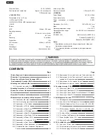
AMPLIFIER SECTION

RMS output power

THD 10%, both channels driven

1 kHz

(Low channel)

75 W per channel (5

)

10 kHz

(High channel)

70 W per channel (5

)

80 Hz

(Subwoofer channel)

160 W (8

)

Total power output

450 W

PMPO

4000 W

FTC output power

THD 10%, both channels driven

100 Hz-3 kHz

(Low channel)

59 W per channel (5

)

3 kHz-10 kHz

(High channel)

57 W per channel (5

)

50 Hz-100 Hz

(Subwoofer channel)

130 W (8

)

Total FTC power

362 W

n

FM/AM TUNER, TERMINALS SECTION

Preset station

FM 15 stations

AM 15 stations

Frequency Modulation (FM)

Frequency range

87.9 - 107.9 MHz (200 kHz steps)

87.5 - 108.0 MHz (100 kHz steps)

©

2004 Matsushita Electric Industrial Co. Ltd.. All

rights

reserved.

Unauthorized

copying

and

distribution is a violation of law.

SA-AK631PL

Colour
(S)... Silver Type

Sensitivity

2.5 µV (IHF)

S/N 26 dB

2.2 µV

Antenna terminal(s)

75

(unbalanced)

Amplitude Modulation (AM)

Frequency range

520 - 1710 kHz (10 kHz steps)

Sensitivity

S/N 20 dB (at 1000 kHz)

560 µV/m

Audio performance (Amplifier)

Input sensitivity/Input impedance

Aux

250 mV,14.7 k

Phone jack

Terminal

Stereo, 3.5 mm jack

Mic jack

Terminal

0.7mV, 680

Mono, 3.5 mm

n

CASSETTE DECK SECTION

Track system

4 track, 2 channel

Heads

Record/playback

Solid permalloy head

Erasure

Double gap ferrite head

Motor

DC servo motor

Recording system

AC bias 100 kHz

Erasing system

AC erase 100 kHz

Tape speed

4.8 cm/s

Overall frequency response (+3 dB, -6 dB at DECK OUT)

NORMAL

35 Hz - 14 kHz

S/N ratio

50 dB (A weighted)

CD Stereo System

Specifications

ORDER NO. MD0412590C3

Summary of Contents for SA-AK631PL

Page 1: ... rights reserved Unauthorized copying and distribution is a violation of law SA AK631PL Colour S Silver Type Sensitivity 2 5 µV IHF S N 26 dB 2 2 µV Antenna terminal s 75 Ω unbalanced Amplitude Modulation AM Frequency range 520 1710 kHz 10 kHz steps Sensitivity S N 20 dB at 1000 kHz 560 µV m Audio performance Amplifier Input sensitivity Input impedance Aux 250 mV 14 7 kΩ Phone jack Terminal Stereo...

Page 2: ...ls 2 Stereo FL FR n GENERAL Power Supply AC 120 V 60Hz Power consumption 255 W Power consumption in standby mode 0 38 W Dimensions W x H x D 250 x 330 x 341 mm Mass 7 1 kg Operating temperature range 5 to 35 C Operating humidity range 5 to 90 RH no condensation n SYSTEM SC AK631 PL Music center SA AK631 PL Speaker SB AK630 PL Subwoofer SB WAK630 GCS Notes 1 Specifications are subject to change wit...

Page 3: ...0 17 4 D Transformer P C B 82 17 5 E CD Detect P C B F Spindle Position P C B G CD Loading P C B K Tuner Pack P C B 83 17 6 H Power P C B L Sub Power P C B 84 17 7 I Deck P C B J Deck Mechanism P C B 86 18 Wiring Connection Diagram 87 19 Illustration of IC 痴 Transistors and Diodes 88 20 Terminal Function of IC 痴 89 20 1 IC7002 MN6627953HB Servo processor Digital signal processor Digital filter D A...

Page 4: ...ted if either of the following conditions are noticed No sound is heard when the power is turned on Sound stops during a performance The function of this circuitry is to prevent circuitry damage if for example the positive and negative speaker connection wires are shorted or if speaker systems with an impedance less than the indicated rated impedance of the amplifier are used If this occurs follow...

Page 5: ...to damage ES devices 6 Do not remove a replacement ES device from its protective package until immediately before you are ready to install it Most replacement ES devices are packaged with leads electrically shorted together by conductive foam aluminium foil or comparable conductive material 7 Immediately before removing the protective material from the leads of a replacement ES device touch the pr...

Page 6: ...the short pin finish the job in as short time as possible 4 Do not turn the variable resistor laser power adjustment It has already been adjusted Grounding for electrostatic breakdown prevention 1 Human body grounding Use the anti static wrist strap to discharge the static electricity from your body 2 Work table grounding Put a conductive material sheet or steel sheet on the area where the travers...

Page 7: ...adjust the preset variable resistor on the pickup lens 4 Do not disassemble the optical pick up unit 5 If the optical pick up is replaced use the manufacturer s specified replacement pick up only 6 Use of control or adjustments or performance of procedures other than those specified herein may result in hazardous radiation exposure CAUTION THIS PRODUCT UTILIZES A LASER USE OF CONTROLS OR ADJUSTMEN...

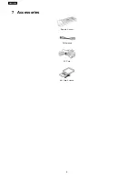
Page 8: ...7 Accessories Remote Control FM Antenna AC Cord AM Loop Antenna 8 SA AK631PL ...

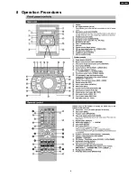
Page 9: ...8 Operation Procedures 9 SA AK631PL ...

Page 10: ...10 SA AK631PL ...

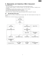
Page 11: ...cement reverse the respective procedures Special reassembly procedures are described only when required 3 Select items from the following index when checks or replacement are required 4 Refer to the Parts No on the page of Parts Location and Replacement Parts List Section 22 if necessary 9 1 Disassembly flow chart The following chart is the procedure for disassemblin g the casing and inside parts ...

Page 12: ...ration of gear for servicing perform the procedures as follows 3 In case of re servicing the same set the gear for servicing may has been taken off because it has been used The gear for servicing must be stored Remove the gear provided with mecha cover as shown below Insert the hexagonal screwdriver 2mm into the gear and then project the tip of screwdriver for 1 2 mm in length 12 SA AK631PL ...

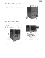
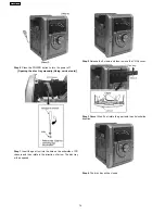
Page 13: ...power cord Step 2 Press the POWER button to power up the main unit Step 3 Press the OPEN CLOSE button the disc tray will open automatically Step 4 Release the 2 claws and then remove the CD Lid Step 5 Press the OPEN CLOSE button the disc tray will close 9 3 Disassembly of Top Cabinet 9 4 Disassembly of CD Lid The CD changer unit can be removed after the CD Lid is removed Follow the Step 1 Step 2 o...

Page 14: ...t the gear tool into the hole on the underside of CD chassis and then rotate in the direction of arrow The disc tray will be opened Step 2 Release the 2 claws and then remove the CD lid cover Step 3 Repeat Step 2 but rotate the gear tools in anti clockwise direction Step 4 The disc tray will be closed 14 SA AK631PL ...

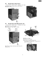
Page 15: ...t up the CD Mechanism Unit Step 4 Remove 4 screws Step 5 Remove the CD chassis Step 6 Lay the CD mechanism unit as shown For disassembly of CD mechanism unit please refer to Section 9 13 of this manual 9 5 Disassembly of Rear Panel Follow the Step 1 Step 2 of Item 9 3 Disassembly of Top Cabinet 9 6 Disassembly of CD Mechanism Unit Follow the Step 1 Step 2 of Item 9 3 Disassembly of Top Cabinet 15 ...

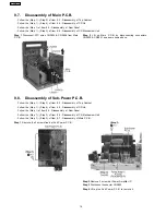
Page 16: ...of Item 9 3 Disassembly of Top Cabinet Follow the Step 1 Step 6 of Item 9 4 Disassembly of CD Lid Follow the Step 1 of Item 9 5 Disassembly of Rear Panel Follow the Step 1 Step 3 of Item 9 6 Disassembly of CD Mechanism Unit 9 8 Disassembly of Sub Power P C B Follow the Step 1 Step 2 of Item 9 3 Disassembly of Top Cabinet Follow the Step 1 Step 6 of Item 9 4 Disassembly of CD Lid Follow the Step 1 ...

Page 17: ...he Power P C B with insulation material to avoid short circuit 9 9 Disassembly of Power P C B Follow the Step 1 Step 2 of Item 9 3 Disassembly of Top Cabinet Follow the Step 1 Step 6 of Item 9 4 Disassembly of CD Lid Follow the Step 1 of Item 9 5 Disassembly of Rear Panel Follow the Step 1 Step 3 of Item 9 6 Disassembly of CD Mechanism Unit Follow the Step 1 Step 2 of Item 9 7 Disassembly of Main ...

Page 18: ...ansistor and replace the components Step 4 Fix back the cut portion with a screw as shown Replacement of the Power Amplifier IC Voltage Regulator 9 10 Disassembly of Transformer P C B Follow the Step 1 Step 2 of Item 9 3 Disassembly of Top Cabinet Follow the Step 1 Step 6 of Item 9 4 Disassembly of CD Lid Follow the Step 1 of Item 9 5 Disassembly of Rear Panel Follow the Step 1 Step 3 of Item 9 6 ...

Page 19: ... CN2803 and CN5950 9 11 Disassembly of Front Panel Unit Follow the Step 1 Step 2 of Item 9 3 Disassembly of Top Cabinet Follow the Step 1 Step 6 of Item 9 4 Disassembly of CD Lid Follow the Step 1 Step 3 of Item 9 6 Disassembly of CD Mechanism Unit 9 12 Disassembly of Deck Mechanism Unit Follow the Step 1 Step 2 of Item 9 3 Disassembly of Top Cabinet Follow the Step 1 Step 6 of Item 9 4 Disassembl...

Page 20: ... Mechanism P C B Step 6 Remove 3 screws Step 7 Unsolder the motor terminals Step 8 Remove Deck Mechanism P C B Step 3 Rotate the hexagonal wrench in the direction of arrow clockwise and then open the disc tray fully 9 13 CD Mechanism Main Component Replacement Procedures Follow the Step 1 Step 2 of Item 9 3 Disassembly of Top Cabinet Follow the Step 1 Step 6 of Item 9 4 Disassembly of CD Lid Follo...

Page 21: ...the direction of arrow 2 Step 6 Lift up the traverse deck ass y Step 7 Remove the traverse deck ass y from the timing lever Caution When removing or inserting the traverse deck avoid touching the OPU lens and pressing onto the turntable Step 8 Remove 3 screws Step 9 Unsolder the motor terminals 4 points Step 10 Remove the FFC board from the connector and then remove the CD Servo P C B 21 SA AK631P...

Page 22: ...Installation of the CD Servo P C B after replacement Step 1 Connect the FFC board Step 2 Install the CD servo P C B in the traverse deck ass y Step 3 Remove 3 screws Step 4 Solder Note for installation of the CD servo P C B Installation for traverse deck ass y Step 1 Install the traverse deck ass y to the timing lever Step 2 Align the boss of traverse deck ass y with the slot of traverse cam gear ...

Page 23: ...h lifting the claw in the direction of 1 draw the CD Detect P C B in the direction of arrow 2 Step 4 Force the disc tray fully Step 5 With pressing the claw B in the direction of arrow 1 force the connection lever in the direction of arrow 2 Step 5 Remove the mechanism cover 9 13 2 Replacement for the Disc Tray 23 SA AK631PL ...

Page 24: ...laws and then draw the disc tray Step 9 With forcing the left guide bar manually because the left guide bar interfers with claw draw the disc tray Installation of the disc tray after replacement Step 1 Slide the drive rack fully in the direction of arrow Step 2 Holding the drive rack not to move install the disc tray Step 3 Align the drive rack with the drive gear 24 SA AK631PL ...

Page 25: ...r spring Step 4 Remove the pulley gear change gear and UP DOWN gear NOTE Force the right guide bar of tray base manually not to move upwards Step 4 Holding the disc tray manually push the disc tray in the direction of the arrow Step 5 Release the 2 claws and then remove the bottom SW P C B 9 13 3 Disassembly and reassembly for mechanism base drive unit 25 SA AK631PL ...

Page 26: ...he claw and then remove the tray lock Step 8 Release the claw and then remove the rear lock Step 9 Pressing the claw B in the direction of arrow 1 force the connection lever in the direction of arrow 2 Step 10 Move the slide plate 1 to the end of stock side 26 SA AK631PL ...

Page 27: ...n of arrow 2 Step 12 Remove slide plate 1 and slide plate 2 Step 13 Remove the traverse relay gear traverse cam gear and drive gear Dissassembly reassembly for the spindle base unit Step 1 Draw the 5 disc spacers Step 2 Pushing the claw slide the support plate in the direction of arrow and then remove it 27 SA AK631PL ...

Page 28: ... disc lever spring Step 4 Release the 2 claws and then draw the relay gear B Step 5 Release the 2 claws as shown below NOTE Hold the loading stopper ass y manually bacause it is flipped by spring Step 6 Remove the cushion spring Step 7 Remove the loading stopper ass y in the direction of arrow 28 SA AK631PL ...

Page 29: ...ewdriver Step 12 Squeeze the shaft of lower hook and then draw it Step 13 Rotate the lower spindle in the direction of arrow until the lower spindle interferes with stopper Step 14 Insert the thin tip of minus screwdriver between the lower spindle and UP DOWN base and then slacken the lower spindle to release the stopper Then rotate the lower spindle and remove it Step 15 Rotate the UP DOWN base a...

Page 30: ... the loading stopper ass y and then align the lower spindle with the trapezoid tooth of relay gear A Step 3 Force the loading stopper ass y latch the claw firmly Reassembly for mechanism base drive unit Step 1 Install the traverse cam gear Step 2 Rotate the traverse cam gear to the direction of arrow Step 3 Install the drive gear and traverse relay gear When installing the traverse relay gear alig...

Page 31: ...n leve and align the trapezoid tooth of traverse relay gear with the slide plate 1 Step 6 Install the spindle base unit First slide plate 1 Step 7 Move the slide plate 1 to forward fully Step 8 Install the rear lock The claw should be latched Step 9 Install the Spindle Position P C B The claw should be latched Step 10 Install the tray lock The claw should be latched 31 SA AK631PL ...

Page 32: ...ll the gear holder and then tighten the screw a Step 14 Install the tray base traverse ass y mechanism cover and upper plate Operation check after servicing Check the proper operation of following items with gear and hexagonal screwdriver 1 Open close of tray base 2 Moving the tray base to the stock side 3 UP DOWN operation of spindle base unit 4 UP DOWN operation of traverse ass y 32 SA AK631PL ...

Page 33: ...r terminals 2 points Step 5 Unsolder the motor terminals 2 points Step 6 Release the 2 claws A and then remove the Motor P C B Step 7 Release the claw B and then remove the motor ass y Notice for motor ass y installation 1 Locate the name plate of motor to the traverse ass y 2 Align the hole of motor with the ribs 9 13 4 Replacement for the motor ass y 33 SA AK631PL ...

Page 34: ...ve 2 screws 9 14 Replacement for the pinch roller ass y and head block Follow the Step 1 Step 2 of Item 9 3 Disassembly of Top Cabinet Follow the Step 1 Step 6 of Item 9 4 Disassembly of CD Lid Follow the Step 1 Step 3 of Item 9 6 Disassembly of CD Mechanism Unit Follow the Step 1 Step 3 of Item 9 11 Disassembly of Front Panel Unit Follow the Step 1 Step 5 of Item 9 12 Disassembly of Deck Mechanis...

Page 35: ...f the belt Step 1 The boss and marking should be positioned horizontally 9 15 Replacement for the Deck motor ass y capstan belt A capstan belt B and winding belt Follow the Step 1 Step 2 of Item 9 3 Disassembly of Top Cabinet Follow the Step 1 Step 6 of Item 9 4 Disassembly of CD Lid Follow the Step 1 Step 3 of Item 9 6 Disassembly of CD Mechanism Unit Follow the Step 1 Step 3 of Item 9 11 Disasse...

Page 36: ... Step 5 Install the winding lever and spring while pressing the winding arm in the direction of arrow Step 6 Install the flywheel R Step 7 Put the capstan belt A temporarily as shown below Step 8 Put the capstan belt B on the motor ass y pulley Step 9 Install the sub chassis to the mechanism and then tighten screws 36 SA AK631PL ...

Page 37: ...Step 10 Remove 3 screws Step 11 Put the capstan belt B as shown below Step 12 Put the capstan belt A on the motor ass y pulley 37 SA AK631PL ...

Page 38: ...assette lid ass y For DECK1 and DECK2 Step 2 Push up the cassette lid ass y in the direction of arrow For DECK1 and DECK2 9 16 Replacement for the cassette lid ass y Follow the Step 1 Step 2 of Item 9 3 Disassembly of Top Cabinet 38 SA AK631PL ...

Page 39: ...oller during playback or recording rotate the flywheel F in the direction of the arrow to remove it Step 2 Push the lever upward and open the cassette lid ass y Remove the cassette tape 9 17 Rectification for tape jam problem Follow the Step 1 Step 2 of Item 9 3 Disassembly of Top Cabinet 39 SA AK631PL ...

Page 40: ...chanism P C B Sub Power P C B and Power P C B can be carried out using below procedures For the disassemblin g procedures refer to Section 9 10 1 Checking of Main P C B 1 Remove Top Cabinet and Rear Panel 2 Remove CD Lid 3 Disassemble CD Mechanism Unit 4 Connect FFC wires CN2801 CN2805 from CD Mechanism Unit 40 SA AK631PL ...

Page 41: ...10 2 Checking of Transformer P C B 1 Remove Top Cabinet and Rear Panel 2 Remove CD Lid 3 Disassemble CD Mechanism Unit 4 Connect FFC wires CN2801 CN2805 from CD Mechanism Unit 41 SA AK631PL ...

Page 42: ...isassemble Panel P C B 6 Disassemble Deck Mechanism Unit 7 Use the extension cable A to reconnect CN1001 Deck P C B and CN2803 Main P C B 8 Use the extension cable B to reconnect CP6401 Panel P C B and CN971 Deck Mechanism P C B Service Tools Extension FFC A Deck P C B Main P C B REEX0485 14 Pins B Panel P C B Deck Mechanism P C B REEX0484 10 Pins 42 SA AK631PL ...

Page 43: ...terial to avoid short circuit 8 Use the extension cable A to reconnect CN1001 Deck P C B and CN2803 Main P C B 9 Use the extension cable B to reconnect CP6401 Panel P C B and CN971 Deck Mechanism P C B 10 Use the extension cable C to reconnect H5950 W5950 Power P C B and CN5950 Transformer P C B Service Tools Extension FFC A Deck P C B Main P C B REEX0485 14 Pins B Panel P C B Deck Mechanism P C B...

Page 44: ...ith the erasure prevention tab remove from right side only and close the cassette holder 5 Press REVERSE FM MODE BP Tape will be stop after 2 seconds 6 Load a pre recorded tape with both side record tabs intact and close the cassette holder 7 Press PLAY TUNE TIME ADJ UP After TPS function tape will stop automatically 8 Press REC STOP Tape will not move 9 Press STOP TUNE MODE to indicate Error code...

Page 45: ...confirmed in the abnormal detection mode explained in the later section 11 8 2 Abnormality detection for CD Changer block No Abnormal Items Error Display Method of Detection 1 REST SW abnormal F15 Under normal operation Self Diagnostic Mode inclusive this error occurs when the REST SW ON is not detected within the specified time and shall be memorized 2 Transmission error between CD servo LSI and ...

Page 46: ...ode a During cold start of micro processor IC b Restart of aging mode for the mechanism unit 3 Mechanism Error Code Mechansim Error Code Table Error Code Description M 00 No Error M 01 OPEN Position Horizontal Motion Abnormality at play position M 02 PLAY Position Horizontal Motion Abnormality at stock position M 03 PLAY Position Horizontal Motion Abnormality during changing position M 04 CHANGE P...

Page 47: ...CD PLAY mode 12 3 CD Mecha Aging Test Mode CR20 1 Functional summary of CD aging test mode It is for the purpose to determine the reliability of the CD changer 2 To enter into CD aging test mode a First enter into self diagnost ic mode Refer to Section 11 2 How to enter the Self Diagnostic Function b In the self diagnost ic mode switch the SELECTOR to and press It will enter into CD aging test mod...

Page 48: ...M checksum and Version Display Mode a Enter into Self Diagnostic Mode Refer to Section 11 2 b In the Self Diagnostic Mode Press twice The version number and the calculated ROM Checksum of the current software will be displayed on the FL as shown in this example Note The Software Version No Micon Software Checksum differs from set to set The ROM Checksum is calculated on demand not hard coded The R...

Page 49: ...CK 2 FWD Fig 1 13 1 2 Bias and Erase Voltage Check 1 Set the unit AUX position 2 Insert the Normal blank tape QZZCRA into DECK 2 and the unit to REC mode use l REC STOP key 3 Measure and make sure that the output is within the 1 Connect the instrument as shown in Fig 5 2 Set the unit to AM mode 3 Apply signal as shown in Fig 5 from AM SG 4 Adjust Z2602 so that the output frequency is maximized in ...

Page 50: ...Adjust Z2602 OSC so that the EVM AC is maximized 6 Set AM SG to 600Hz 7 Receive 600Hz in the unit 8 Adjust Z2602 ANT so that the EVM SG is maximized 13 3 1 Cassette Deck Section 13 3 2 Tuner Section 9 Set AM SG to 520kHz 10 Receive 520kHz in the unit 11 Adjust L2602 OSC so that the EVM DC value is with 1 1 0 5V Fig 7 13 3 Alignment Points 50 SA AK631PL ...

Page 51: ...COIL DRIVE TRAVERSE MOTOR DRIVE SPINDLE MOTOR DRIVE MUTE CH2 FOCUS COIL TRACKING COIL D4 17 D4 16 D3 15 D3 14 D1 11 D1 10 D2 13 D2 12 4 PC2 3 IN2 6 IN1 24 IN3 23 IN4 1 RST NC 18 5 NC 2 NC B B B B IC7003 AN8739SBTE2 FOCUS COIL TRACKING COIL TRAVERSE MOTOR SPINDLE MOTOR DRIVE M7301 TRAVERSE MOTOR E F B A LPD LD C D SPPOL SPOUT TRVP TRP FOP B B A B F E M M 51 SA AK631PL ...

Page 52: ... VREF 27 A B C D E F 30 35 A B C D E F CEA 21 LD 29 LD PD 28 LPD DCDET 36 CAGC 41 2 EXT1 3 EXT2 76 GIO0 77 GIO1 78 GIO2 75 TXTCK PORT ARF RFOUT 39 RFIN 40 FEN 24 TEN 25 FEOUT 23 TEOUT 26 LRCK BCLK SRDATA SERIAL OUTPUT INTERFACE REGULATOR LON DVDD2 MP3 WMA DECODER FS CONVERTER DIGITAL FILTER 1 BIT DAC PWM LOGIC ANALOG LOWPASS FILTER RFENV 22 A D CONVERTER ADPVCC 18 FEIN 20 TEIN 19 RFENV 22 OUTPUT P...

Page 53: ... FF VCO AM MIX AM RM AMP AGC PHASE DET PILOT DET FF PILOT CANCEL FM TUNER 15V SUPPLY SWITCH Q2606 POWER ON RESET UNIVERSAL COUNTER UNLOCK DETECTOR PHASE DETECTOR CHARGE PUMP TO CDDRIVE BLOCK LC72131MDTRM PLL FREQUENCY SYNTHESIZER IC2602 X2602 16 17 18 11 15 19 10 7 6 9 8 4 CL 3 DI 2 CE 5 DO 13 12 14 20 1 L2602 D2602 L2601 23 24 22 21 20 19 18 17 16 14 15 13 1 2 3 4 6 5 7 8 9 10 11 12 FM IF AMP Q26...

Page 54: ...XOUT 12 RMT 18 MLD 79 MDATA 80 MCLK 81 22 SD 77 21 ST DO 78 STATUS 84 CHG_CW 85 CHG_CCW 88 CHG_PLR 83 CHG_HLF 89 CHG_AD2 90 CHG_AD1 86 CHG_SW1 87 CHG_SW2 PLLCE 3 30 PLLCK 29 PLLDA X_IN 15 X_OUT 13 V_JOG_A 67 V_JOG_B 68 RESTSW 82 IN1 5 IN2 6 VREF 4 VCC 7 GND 1 10 OUT2 2 OUT1 8 VS D2 X2802 XC_IN 10 XC_OUT 11 X2801 19 BLKCK P1 50 84 P35 G1 7 14 30 37 G16 D15 S34 FL6601 FL DISPLAY SW1 PUSH SW3 OPEN B ...

Page 55: ...ER ON OFF SWITCH SSEQ_LED 76 D6457 95 PHOTO_2 IC951 CNB13030R2AU PHOTO INTERRUPTER 97 PHOTO_1 56 PLG1 Q6411 Q6421 57 PLG2 60 DECK1_H 10 16 14 13 11 6 19 15 12 21 4 22 3 17 8 1 2 24 23 18 7 9 3 5 2 4 59 REC Q2980 DECK MOTOR SWITCH 58 MTR 20 5 M1002 S951 MODE 52 HALF_1 53 MODE_1 S952 HALF Z971 INTERFACE 91 DECK2 S972 HALF S975 RECINH_F S971 MODE D971 DECK 2 R P HEAD LCH Q6456 LED DRIVE SW_LED 54 D64...

Page 56: ... 12 B D2811 40 MUTE_A 39 MUTE_H IC2804 C0AABA000009 DUAL OP AMP AGC CONTROL Q2571 MUTING SWITCH 23 HARMONIC_SW 7 1 3 5 6 2 IC2806 C0ABBB000244 DUAL OP AMP IC2805 C0ABBB000244 DUAL OP AMP 1 7 5 3 2 6 D2813 SWITCH Q2902 D2901 Q2901 1 2 LM_L R SWITCH C3EBDG000052 E EPROM NOT SUPPLIED IC2802 5 4 3 43 EE_DAT 42 EE_CLK 41 EE_CS 6 SW_LV1 24 SW_LV1 SW_LV2 25 SW_LV2 IC2808 C0ABBB000244 DUAL OP AMP Q2806 PO...

Page 57: ...SYNC DC_DET FAN MUTE_H SW_LV1 SWITCH Q2551 SUBWOOFER LEVEL CONTROL Q2553 SW_LV2 SWITCH Q2552 SUBWOOFER LEVEL CONTROL Q2554 C0ABBB000244 DUAL OP AMP IC2810 SUBW HP_SW FILTER 1 7 5 3 2 6 57 SA AK631PL ...

Page 58: ...Q5805 Q5803 Q5801 IN GND 14 OUT GND 11 10 VCCM Q5814 HEADPHONE MUTING SWITCH D5813 18 VD 5 1 VCC 1 2 17 VD 4 2 VCC 1 2 B 7 9 OUT 1 1 2 3 6 OUT 2 1 2 IN1 1 2 13 12 IN2 1 2 16 15 SYNCHRONISING SWITCH D5814 JK5851 JK5852 Z5950 RSN35H2B P POWER HIC IC5002 AC DET 6 VCCM 8 LATCH 5 OUT_L R 4 1 IN_L R 10 14 8 AC DET D5950 D5953 D5970 D5973 SUBW MAIN SIGNAL LINE FM OSC SIGNAL LINE FM SIGNAL LINE CD SIGNAL ...

Page 59: ...15 Voltage Measurement 59 SA AK631PL ...

Page 60: ...60 SA AK631PL ...

Page 61: ...201 Rest switch VR6491 VR Volume Jog VR6511 VR Mic Volume The voltage value and waveforms are the reference voltage of this unit measured by DC electronic voltmeter high impedance and oscilloscope on the basis of chassis Accordingly there may arise some error in voltage values and waveformsdepending upon the internal impedance of the tester or the measuring unit Importance safety notice Components...

Page 62: ...352 0 01 R7327 1 5K R7335 100 C7335 0 1 C7334 10V220 R7336 10 F C7670 0 1 R7315 2 7K R7325 560 C7315 0 22 SCHEMATIC DIAGRAM 1 CD SERVO CIRCUIT OPTICAL PICKUP CIRCUIT B SIGNAL LINE M M 12 11 10 2 4 6 8 9 7 5 3 1 13 14 15 16 IC7003 VCC NC NC RSTIN IN3 IN4 VREF NC RST GND GND PVCC2 PGND2 D4 D4 D3 D3 PGND1 PVCC1 NC D2 D2 D1 D1 IN1 NC PC2 NC IN2 NC 3 4 5 6 24 25 26 8 1 2 23 21 9 20 10 19 11 18 12 13 17...

Page 63: ...D2 NTEST CAGC PLFF0 ARFOUT AVSS2 ARFIN DSLF IREF PLLF AVSS1 NC OUTR IOVDD1 REGON IOMODE DVSS2 AVDD1 OUTL DVDD2 1 2 3 4 5 6 7 8 9 10 11 12 13 14 15 16 17 18 19 20 21 22 23 24 25 26 27 28 29 30 31 32 33 34 35 36 37 38 39 40 41 42 43 44 45 46 47 48 49 50 51 52 53 54 55 56 57 58 59 60 64 61 62 63 68 65 66 67 72 69 70 71 73 74 75 76 77 78 79 80 STAT TX MAIN CIRCUIT CN2801 ON SCHEMATIC DIAGRAM 5 29 C710...

Page 64: ...22K R2602 4 7K C2639 50V4 7 C2619 680P C2618 0 01 C2617 0 01 C2642 50V1 R2642 6 8K C2641 50V1 R2641 6 8K R2626 1K R2625 470 R2629 27K R2627 470 C2624 100P R2632 10K C2648 0 01 R2624 33 X2602 H3F1065A0002 C2622 50V1 R2622 2 7K C2621 50V0 47 R2631 120 R2644 120 R2633 1K C2629 6 3V100 C2649 0 1 C2623 50V1 R2645 100K C2643 6800P C2644 6800P R2646 100K TO MAIN CIRCUIT 2A ON SCHEMATIC DIAGRAM 8 1A 1B 1 ...

Page 65: ... B REC_H 15V RECINR RECINL AFGND PBR PBL MOT10V REC 15V REC_R REC_L PBR PBL JK2801 RCH AUX LCH R2216 12K R2217 2 7K C2217 100P C2216 680P R2116 12K R2117 2 7K C2117 100P C2116 680P AUXL C2998 0 1 9V R2192 0 R2191 1K C2192 0 R2193 100K C2193 0 1 R2292 0 R2291 1K C2292 0 R2293 100K C2293 0 1 C2194 16V10 R2197 1K LO_L C2294 16V10 R2297 1K LO_R Q2181 C2182 8200P C2181 8200P R2183 5 6K HI_L C2183 1 R21...

Page 66: ... DECK2 KEY1 KEY2 KEY3 PHOTO_1 PHOTO_2 RMT VREF SYNC SW5V PCONT SYS6V C2753 0 1 C2999 0 1 R2933 0 D2904 B0EAKM000117 R2903 15 R2902 12 R2901 10K C2903 0 01 R2910 330 R2909 2 2K C2904 16V100 Q2902 R2907 1K R2908 330 R2932 0 D2901 B0ADCC000002 SW5V CD8V R2918 10K R2924 10K C2201 1 C2101 1 R2201 1 2K R2101 1 2K R2102 1 8K R2202 1 8K C2202 0 1 C2102 0 1 C2203 1000P C2103 1000P LCH RCH R2919 4 7K Q2906 ...

Page 67: ...B SIGNAL LINE R2561 3 3K 16V10 C2556 0 01 R2564 330K C2555 100P R2565 3 9K R2563 C2558 0 15 C2559 47P C2560 1 R2566 2 2K C2557 0 01 C2553 0 01 C2554 16V1 IC2810 R2559 18K R2558 3 3K R2556 1K R2557 1K Q2554 Q2553 R2568 100K Q2552 Q2551 SW_LV2 SW_LV1 R2562 47K D2551 B0BC4R300002 D2552 B0BC4R300002 22K C2551 R2560 47K C2561 1 9V R2555 1K SUBW 1 2 7 8 3 6 4 5 IC2810 C0ABBB000244 DUAL OP AMP Q2553 Q255...

Page 68: ...841 10K REC MTR DECK1_H PLG2 PLG1 MODE_1 HALF_1 MLD CD_RST SSEQ_LED EXP_DAT EXP_CLK V_JOG_B V_JOG_A VCC R2892 0 C2821 100P D2802 B0ADCJ000020 R2803 10K R2802 100 R2891 47K C2854 16V100 C2852 16V100 SYS6V RMT BLKCK SYNC DO ST ASP_DAT ASP_CLK LM_L VCC XC_IN XC_OUT X_OUT XIN C2851 C2853 0 1 Q2806 Q2806 B1GBCFJJ0039 POWER RESET CONTROL SWITCH D2804 B0ACCK000005 C2857 50V2 2 VREF C2841 18P C2840 18P R2...

Page 69: ...2317 100K C2120 1 C2412 0 15 C2411 0 18 R2418 2 7K R2417 100K C2220 1 R2111 10K R2112 22K C2111 0 1 C2112 1500P R2211 10K R2212 22K C2211 0 1 C2212 1500P R2206 100 C2206 3300P R2952 4 7K C2121 0 1 C2221 0 1 R2103 6 8K C2126 0 1 C2226 0 1 R2108 6 8K C2131 0 22 C2231 0 068 R2113 10K C2136 0 22 C2236 0 068 R2118 10K OUT1 OUT2 C2583 0 22 ASP_CLK R2586 1 2K SW5V R2584 330K C2584 220P R2585 330K C2585 2...

Page 70: ...2 MOT10V MODE_1 PL2 PL1 DECK2 HALF MODE_1 VREF_GND PGND 1 2 4 6 8 10 9 7 5 3 TO DECK MECHANISM CIRCUIT CN971 ON SCHEMATIC DIAGRAM 15 B SIGNAL LINE Q6421 Q6425 B1GACFLL0007 PLUNGER ON OFF SWITCH K2 MOT10V SSEQ_LED Q6457 S6201 S6203 S6202 S6210 S6209 S6208 S6207 S6206 S6205 S6204 R6203 1K R6204 1 2K R6206 2 2K R6210 10K R6208 4 7K R6209 6 8K R6207 2 7K R6205 1 8K CD TUNER REW DECK1 OPEN AUX TAPE DEC...

Page 71: ... MIC 9V MIC MIC_GND P23 P24 P25 P26 P27 P28 P29 P30 P31 P32 R6601 C6612 33P R6611 R6602 470 R6603 220 R6604 220 C6601 100P C6621 100P C6623 6 3V47 C6602 1000P C6603 100P C6604 100P C6636 100P FL_CS SW5V FL_RESET FL_CLK FL_DOUT C6631 35V22 C6632 35V22 470 15K P17 P18 P19 P20 P21 P22 1 2 3 4 8 9 10 11 12 13 14 30 31 32 33 34 35 36 37 38 41 42 43 86 85 84 83 82 81 80 79 78 77 76 75 74 73 72 71 70 69 ...

Page 72: ...002 D5966 B0EAKM000117 R5956 10 R5955 10 R5954 10 Q5950 D5963 B0EAKM000117 C5953 0 01 Q5950 B1BACD000017 SYSTEM 6V VOLTAGE REGULATOR C5952 10V47 R5953 150 R5952 1K C5961 10V470 D5964 B0BA6R600008 D5962 C5963 35V4 7 R5958 10K R5957 10K C5954 0 01 C5951 0 01 Q5952 F1 125V 4 0A FC2 FC1 JK5950 FL2 VP FL1 SYS6V SYS6V PCONT SYNC D_GND ST_GND TO POWER CIRCUIT H5950 W5950 ON SCHEMATIC DIAGRAM 13 Q5951 Q59...

Page 73: ...C1 C0GAM0000005 MOTOR DRIVE NC V S SCHEMATIC DIAGRAM 12 B SIGNAL LINE B SIGNAL LINE SUB POWER CIRCUIT IC5002 RSN35H2B P POWER HIC 1 2 3 4 5 6 7 8 9 10 11 12 13 14 IN_R IN_R IN GND IN_L IN_L GND VCCM MUTE C AC DET LATCH OUT_L VCC VCC OUT_R IC5002 C5758 2200P C5658 2200P D5003 D5003 B0BC01000006 C5018 100V10 C5019 100V10 R5036 330K H5004 W5004 TO POWER CIRCUIT CN5803 ON SCHEMATIC DIAGRAM 13 C5777 39...

Page 74: ... CIRCUIT PROTECTION Q5804 Q5804 B1BCCG000002 CURRENT STABILISER SWITCH R5830 1 2K Q5807 Q5807 B1ABCF000131 10V VOLTAGE REGULATOR E5800 JK5852 H5950 W5950 R5829 330 C5812 25V33 D5809 B0BC01000014 D5805 C5809 0 01 D5804 B0ACCK000005 D5807 R5831 2 2K R5882 150 D5808 B0BA5R600003 C5864 0 01 Q5808 Q5808 B1BACD000017 5V VOLTAGE REGUALTOR TO TRANSFORMER CIRCUIT CN5950 ON SCHEMATIC DIAGRAM 11 Q5803 B1BACG...

Page 75: ...GC000007 SWITCHING RECH Q1007 R1090 220 C1046 16V220 R1040 0 C1044 10V33 R1004 1 5K Q1004 Q1005 Q1004 Q1005 B1AAGC000007 BIAS OSCILLATOR C1013 1000P C1014 1000P C1010 25V100 R1007 4 7 C1016 2200P C1017 2200P R1011 10K Q1007 B1ABCF000131 BIAS OSC CONTROL C1026 6 3V47 R1013 4 7K R1012 4 7K C1018 0 01 R1014 4 7K C1011 0 047 C1008 50V1 C1034 50V3 3 R1032 10K R1055 2 2K C1038 220P C1042 16V22 R1031 27K...

Page 76: ...TO INTERRUPTER Z971 RGSD12A1445T MODE PL GND HALF STBY_5V VREF_GND PHOTO_T D1_CRO2 TO PANEL CIRCUIT CP6401 ON SCHEMATIC DIAGRAM 9 MODE PL GND HALF PHOTO_S STBY_5V VREF_GND PHOTO_T D1_CRO2 DECK MECHANISM CIRCUIT CN971 PL1 PL2 STBY_5V PL_GND AD_OUT PHOTO_PB PHOTO_RP HALF_PB VREF_GND MODE_PB R972 820 R973 39K PL971 R952 820 R953 39K D951 MA2C16500E D971 MA2C16500E PL970 S952 HALF S951 MODE S972 HALF ...

Page 77: ...W7040 W7042 W7043 C7107 W7003 W7002 W7004 R7323 R7331 C7338 R7325 R7315 C7315 R7335 R7327 R7349 C7339 R7339 R7328 C7352 R7329 W7001 W7008 W7019 W7005 W7027 W7009 W7007 W7011 C7217 C7155 W7012 W7013 W7014 W7015 W7016 W7017 C7161 W7028 C7224 W7018 W7044 W7023 W7020 W7021 W7024 W7025 C7166 R7254 C7263 C7264 W7010 C7626 W7022 W7050 W7051 W7052 W7053 W7054 W7055 C7614 C7334 C7601 C7203 C7223 C7231 C723...

Page 78: ...456 W2457 W2455 W2454 W2343 W2342 W2344 W2341 W2338 C C2976 W2351 W2340 W2339 W2348 W2169 C2582 W2369 W2353 W2354 W2355 W2360 W2356 W2373 W2389 W2388 W2387 W2386 W2382 W2381 W2377 W2376 W2375 W2384 W2380 W2374 W2385 W2461 W2152 CN2809 JK2801 W2147 W2151 W2168 W2128 W2127 W2126 W2136 W2141 W2137 W2131 W2132 W2121 W2119 W2130 C2245 C2251 C2151 W2101 W2111 W2108 W2109 W2113 W2114 W2115 W2102 W2117 W2...

Page 79: ...2131 C2226 C2126 R2417 R2317 R2418 R2318 C2120 D2811 D2813 R2899 R2571 W2919 CN2801 W2262 X2802 W2227 W2260 W2259 W2258 W2279 W2275 W2265 W2209 W2263 W2282 W2283 X2801 W2277 W2228 W2287 56 W2293 W2291 55 W2284 W2267 W2266 W2301 W2297 C2852 C2902 Q2902 Q2901 C2904 W2276 W2223 W2292 W2299 W2300 W2290 W2289 C2857 W2280 W2281 C2905 W2270 W2271 W2273 W2272 W2269 W2268 W2208 C2854 W2286 W2226 W2207 W229...

Page 80: ...6103 R6105 R6106 R6107 R6108 R6110 R6109 C6551 C6552 W6001 C6553 W6035 C6631 W6007 C6623 W6036 C6635 D6635 R6632 R6631 CP6401 R6403 R6404 R6416 R6411 R6415 R6412 Q6425 Q6421 R6425 R6421 R6405 W6037 W6067 W6008 W6009 W6039 W6040 W6011 W6041 C6481 W6012 W6013 W6070 W6024 W6061 C6491 C6492 R6492 W6025 R6491 W6026 W6088 W6027 W6028 W6029 W6030 W6015 W6044 W6045 W6016 W6017 W6018 W6019 W6046 W6021 W600...

Page 81: ...34 W6075 W6076 W6080 W6065 C6632 421 R6405 W6037 R6402 W6066 W6085 W6077 W6067 W6068 R6458 W6010 W6069 W6060 W6086 R6401 R6406 W6039 W6040 W6023 W6070 C6492 R6492 R6491 R6493 R6457 Q6457 Q6456 R6456 W6003 W6071 W6073 W6042 W6043 W6031 W6020 W6078 W6049 W6050 W6094 W6081 W6059 W6091 W6090 W6082 W6083 W6033 W6089 W6063 C6636 FL6601 W6093 W6092 R6604 C6621 C6602 R6602 R6601 C6601 C6603 C6604 R6603 R6...

Page 82: ...5918 W5940 C5955 C5957 C5956 W5920 W5987 W5990 W5988 W5989 C5963 R5957 R5952 R5958 R5951 R5961 R5960 Q5953 Q5950 JK5950 RL5950 W5995 FC2 T5951 SUB TRANSFORMER R5956 R5955 R5954 FP5951 1A FP5950 4A W5963 W5962 Q5952 W5959 D5960 D5962 D5964 D5961 D5958 D5966 D5959 D5955 D5956 D5965 Q5951 C5953 C5958 C5951 C5954 C5960 C5959 C5952 C5950 CN5951 D5950 D5953 D5951 D5972 Z5950 W5903 W5904 W5938 D5952 D597...

Page 83: ...D E F G 1 2 3 4 5 6 7 8 9 F G E K PbF PbF PbF D1 R1 C1 Q1 R4 Q2 L1 R6 R5 D2 C3 C4 C5 C6 C7 C8 C9 C10 C11 R7 R8 R9 R10 Q3 Q4 D3 R11 L2 C2 R3 R2 J1 J2 J3 J4 CD W2 SW4 D1 W1 SW5 LOAD IC1 J3 J1 SW3 OPEN R1 D2 Q1 SW1 PUSH W2 W1 CN1 C2 J4 C1 J2 1 2 M SW2 PUSH 3 4 PbF 1 2 3 4 5 6 7 8 9 10 1 C 1 2 2 3 4 5 6 7 8 9 10 11 12 13 14 3 E B 1 2 3 E C A CA 1 2 3 4 A CA A G S D A CA A A CA A B C E B C E B C E 83 S...

Page 84: ... C5864 W5806 W5805 W5812 D5805 D5807 C5813 W5872 W5809 W5810 C5812 W5819 W5824 R5827 R5826 R5825 Q5805 CN5801 C5810 R5824 W5823 C5807 W5826 W5846 W5829 W5827 W5832 W5833 W5835 W5836 W5873 W5839 W W5841 C5808 C5805 W5830 H5950 W5950 C5840 C5820 Q5801 Q5802 Q5803 Q5804 IC5801 E5800 R5848 R5846 FP5833 0 4 R5845 R5816 R5809 R5808 R5807 R5815 R5829 R5834 R5844 R5843 W5843 CN5 W5825 W5828 W5844 W5838 W5...

Page 85: ...854 R5855 R5856 R5857 R5671 R5771 R5246 Q5813 Q5812 R5806 C5803 R5853 R5772 C5444 C5445 C5244 C5245 C5449 C5450 C5249 C5250 D5820 D5802 C5660 C5662 C5762 C5760 C5252 C5451 W5833 W5835 W5836 W5839 W5842 W5841 CN5800 W5845 W5850 W5851 C5838 C5820 IC5801 W5843 CN5803 W5844 W5853 W5838 W5854 R5773 R5673 R5456 R5455 R5256 JK5851 JK5852 W5856 W5855 C5802 W5834 W5858 W5857 R5255 W5848 W5837 W5847 W5852 W...

Page 86: ...C1019 C1014 C1013 C1057 R1018 R1055 R1032 C1018 R1014 R1012 R1013 R1026 C1015 C1012 C1027 C1058 R1019 C1039 R1030 R1022 R1049 C1050 R1011 Q1007 R1092 R1091 R1050 R1087 R1085 R1086 R1084 R1057 R1031 R1035 R1090 R1017 C1022 R1028 D1004 D1003 R1040 R1098 C1038 C1036 R1015 R1025 R1027 R1020 R1002 C1059 R1024 R1099 R1100 R1101 C1023 TP10 TP11 TP4 TP3 TP5 TP12 x x x x x x C1049 R1029 CN971 S971 MODE S97...

Page 87: ...IS P C B AC VOLTAGE LINE PLEASE DO NOT RISK OF ELECTRIC SHOCK CAUTION D TRANSFORMER P C B SOLDER SIDE T5951 SUB TRANSFORMER T5950 POWER TRANSFORMER CN5951 9 1 9 1 1 9 CN5950 CN5800 CN5803 JK5852 JK5851 H5950 W5950 9 1 CN5801 1 12 1 12 1 9 H POWER P C B SOLDER SIDE RIGHT CHANNEL SPEAKER LEFT CHANNEL SPEAKER SUBWOOFER H5004 W5004 PbF PHONES SENSOR VOLUME MIC MIC VOLUME H6555 W6555 9 1 C PANEL P C B ...

Page 88: ...3NMNTLM 24P LC72131MDTRM 20P C1BB00000732 32P C0HBB0000039 64P C2CBJG000561 100P MN6627953HB 80P 1 4 8 5 C0AABA000009 C1AA00000612 RSN315H42C P 18P 1 1 5 CNB13030R2AU 2 1 2 4 3 3 1 4 AN8739SBTE2 13 1 26 14 6 20 21 7 C0GAM0000005 1 10 B1AAGC000007 B1GACFGG0004 C0ABBB000244 RSN35H2B P 14P B1ACKD000004 B1AAKD000009 B1AARC000002 B1GCCFJJ0015 B1GCCFGA0005 2SD0592ARA B C E B C E B1AAAC000011 B1AAAD00001...

Page 89: ... I current Reference input 47 PLLF O PLL loop filter 48 PLLF0 O PLL loop filter Pin No Mark I O Function 49 AVDD2 Analog circuit power supply 2 50 OUTL O LCH output signal 51 AVSS1 Audio output circuit GND 1 52 N C No Connection 53 AVDD1 Power supply 1 for analog circuit 54 OUTR O RCH output signal 55 DVSS2 Digital circuit GND 2 56 IOVDD1 I O power supply 1 57 DVDD2 Power supply 2 for Digital circ...

Page 90: ...uner Pin No Mark I O Function 39 MUTE_H O HIC Mute 40 MUTE_A O Audio Mute 41 EE_CS EFP_ EP M O EEPROM Chip Select 42 EE_CLK O EEPROM Clock 43 EE_DAT I O EEPROM Data 44 CD1_LED O CD 1 LED 45 CD2_LED O CD 2 LED 46 PCONT EFP_ CE O Main Transformer Control Output 47 DCDET I DC Detect Input 48 CD3_LED O CD 3 LED 49 CD4_LED O CD 4 LED 50 CD5_LED O CD 5 LED 51 N C No Connection 52 HALF_1 I Deck 1 Half Pl...

Page 91: ...Pin No Mark I O Function 98 VREF Reference for A D 5V 99 AVcc Analog Power Supply Input 100 Demo Selector I H default demo on L default demo off 91 SA AK631PL ...

Page 92: ...21 Troubleshooting Guide 92 SA AK631PL ...

Page 93: ...unless specified otherwise P Pico farads pF F Farads Resistance values are in ohms unless specified otherwise 1K 1 000 OHM The marking RTL indicates that the Retention Time is limited for this items After the discontinuation of this assembly in production the item will continue to be available for a specific period of time The retention period of a availability is dependent on the type of assembly...

Page 94: ...22 1 Deck Mechanism RAA3412 S 22 1 1 Deck Mechanism Parts Location 94 SA AK631PL ...

Page 95: ...95 SA AK631PL ...

Page 96: ... M 118 RML0372 WINDING LEVER M 119 RML0374 EJECT LEVER M 120 RMM0131 BRAKE ROD M 121 RMM0133 1 EJECT ROD M 122 RMQ0519 REEL HUB M 123 RMS0398 1 MOVING CORE M 124 RSJ0003 PLUNGER ASS Y M 125 RMC0061 PACK SPRING M 126 RXF0049 FLYWHEEL F ASS Y M 127 RXF0050 FLYWHEEL R ASS Y M 128 RXG0040 FF RELAY GEAR ASS Y M 129 RMK0283A J SUB CHASSIS M 130 RXL0124 PINCH ROLLER F ASS Y M 130 1 RMB0401 PINCH ARM SPRI...

Page 97: ...22 2 CD Loading Mechanism RD DAC026 S 22 2 1 CD Loading Mechanism Parts Location 97 SA AK631PL ...

Page 98: ...98 SA AK631PL ...

Page 99: ...338 RMR1123 H TRAY M 339 RXQ0595 MOTOR SUB ASS Y M 341 RSJ0003 SOLENOID ASS Y M 343 RMA1106 UPPER PLATE M 344 RML0519 CD LEVER M 345 RFKNAAK27GCS MECHA BASE ASS Y M 346 RML0522 TURNING STOPPER M 347 RMQ0745 LOWER SPINDLE M 348 RMQ0746 UP DOWN BASE M 349 RMB0550 LOWER SPINDLE SPRING M 350 RMQ0747 UPPER HOOK M 351 RME0263 CLICK SPRING M 352 RMQ0743 SPINDLE SHAFT M 353 RMB0552 CUSHION SPRING M 354 RD...

Page 100: ...22 3 Cabinet 22 3 1 Cabinet Parts Location 100 SA AK631PL ...

Page 101: ...101 SA AK631PL ...

Page 102: ...1 TRANSISTOR M Ref No Part No Part Name Description Remarks 18 RKFX0126 1S1 CASS LID R M 19 RKMX0105 S TOP CABINET M 20 RMBX0036 CASS OPEN SPRING M 21 RMCX0021 TRANSISTOR CLIP M 22 RMKX0099 2 BOTTOM CHASSIS M 23 RMKX0100 CD CHASSIS M 24 RMNX0138 FL HOLDER M 25 RMQX0128 VOLUME KNOB ADAPTOR M 26 RUS757ZAA CASS HALF SPRING M 27 RXGX0002 DAMPER GEAR M 28 RXXX0057 K HEAT SINK UNIT M 29 RYFX0138F K1 CD ...

Page 103: ... D5966 B0EAKM000117 DIODE M D5970 B0EAMM000038 DIODE M D5971 B0EAMM000038 DIODE M D5972 B0EAMM000038 DIODE M Ref No Part No Part Name Description Remarks D5973 B0EAMM000038 DIODE M D6456 B3AAA0000583 DIODE M D6457 B3AAA0000583 DIODE M D6458 B3AAA0000583 DIODE M D6635 B0BA7R000005 DIODE M VARIABLE RESISTORS VR6491 EVEKE2F2524M VR VOLUME JOG M VR6511 EVUF2AF15B14 VR MIC VOLUME M SWITCHES S951 K0J1BB...

Page 104: ...ARTH TERMINAL E5800 SNE1004 2 EARTH TERMINAL M WIRES W1 REZ1023 1 4P WIRE M W2 REZ1024 3P WIRE M W1002 RWJ0102050CK MAIN MECHA MOTOR WIRE M W5950 REXX0325 9P FLAT WIRE M W6555 REXX0324 9P FLAT WIRE M CHIP RESISTORS W5004 REXX0457 9P FLAT WIRE M W7001 ERJ3GEY0R00V CHIP JUMPER M W7002 ERJ3GEY0R00V CHIP JUMPER M W7003 ERJ3GEY0R00V CHIP JUMPER M W7004 ERJ3GEY0R00V CHIP JUMPER M W7005 ERJ3GEY0R00V CHIP...

Page 105: ...3V 10K 1 16W M R2146 ERJ3GEYJ102V 1K 1 16W M R2149 ERJ3GEYJ222V 2 2K 1 16W M Ref No Part No Part Name Description Remarks R2152 ERJ3GEY0R00V 0 1 16W M R2154 ERJ3GEYJ104V 100K 1 16W M R2166 ERJ3GEYJ330V 33 1 16W M R2167 ERJ3GEYJ330V 33 1 16W M R2168 ERJ3GEYJ330V 33 1 16W M R2169 ERJ3GEYJ330V 33 1 16W M R2170 ERJ3GEYJ1R0V 1 1 16W M R2171 ERJ3GEYJ332V 3 3K 1 16W M R2181 ERJ3GEYJ332V 3 3K 1 16W M R218...

Page 106: ... M R2615 ERJ3GEYJ561V 560 1 16W M R2616 ERJ3GEYJ102V 1K 1 16W M R2617 ERJ3GEYJ473V 47K 1 16W M Ref No Part No Part Name Description Remarks R2618 ERJ3GEYJ332V 3 3K 1 16W M R2619 ERJ3GEYJ332V 3 3K 1 16W M R2620 ERJ3GEYJ473V 47K 1 16W M R2621 ERJ3GEYJ223V 22K 1 16W M R2622 ERJ3GEYJ272V 2 7K 1 16W M R2623 ERJ3GEYJ683V 68K 1 16W M R2624 ERJ3GEYJ330V 33 1 16W M R2625 ERJ3GEYJ471V 470 1 16W M R2626 ERJ3...

Page 107: ...0T 10 1 2W M R5445 ERJ3GEYJ332V 3 3K 1 16W M R5446 ERJ3GEYJ153V 15K 1 16W M R5447 ERJ3GEYJ332V 3 3K 1 16W M Ref No Part No Part Name Description Remarks R5448 ERJ3GEYJ153V 15K 1 16W M R5449 ERJ3GEYJ683V 68K 1 16W M R5450 ERJ3GEYJ683V 68K 1 16W M R5451 ERJ3GEYJ563V 56K 1 16W M R5452 ERJ3GEYJ224V 220K 1 16W M R5455 ERDS1FVJ100T 10 1 2W M R5456 ERDS1FVJ100T 10 1 2W M R5457 ERDS1FVJ270T 27 1 2W M R563...

Page 108: ...820 1 16W M R7214 ERJ3GEYJ681V 680 1 16W M R7217 ERJ3GEYJ102V 1K 1 16W M R7218 ERJ3GEYJ102V 1K 1 16W M R7220 ERJ3GEYJ105V 1M 1 16W M Ref No Part No Part Name Description Remarks R7221 ERJ3GEYJ101V 100 1 16W M R7253 ERJ3GEYJ100V 10 1 16W M R7254 ERJ3GEYJ102V 1K 1 16W M R7315 ERJ3GEYJ272V 2 7K 1 16W M R7323 ERJ3GEYJ562V 5 6K 1 16W M R7325 ERJ3GEYJ561V 560 1 16W M R7327 ERJ3GEYJ152V 1 5K 1 16W M R732...

Page 109: ...05K 0 16V M C2332 ERJ3GEY0R00V 0 1 16W M C2334 ECUV1C224KBV 0 22 16V M C2401 ECJ1VC1H100J 10P 50V M Ref No Part No Part Name Description Remarks C2402 ECJ1VC1H470J 47P 50V M C2411 ECJ1VB1A184K 0 18 10V M C2412 ECJ1VB1A154K 0 15 10V M C2413 ECJ1VC1H100J 10P 50V M C2414 ECJ1VC1H470J 47P 50V M C2415 ECJ1VB1C105K 1 16V M C2501 ECEA1HKN2R2B 2 2 50V M C2511 ECJ1VB1H223K 0 022 50V M C2512 ECJ1VB1A474K 0 ...

Page 110: ... M C5658 ECJ1VB1H222K 2200P 50V M C5660 ECJ1VB1H104K 0 1 50V M C5662 ECJ1VB1H104K 0 1 50V M Ref No Part No Part Name Description Remarks C5758 ECJ1VB1H222K 2200P 50V M C5760 ECJ1VB1H104K 0 1 50V M C5762 ECJ1VB1H104K 0 1 50V M C5777 ECJ1VC1H390K 39P 50V M C5801 ECJ1VB1H103K 0 01 50V M C5802 ECEA0JKA221B 220 6 3V M C5803 ECJ1VB1H102K 1000P 50V M C5804 ECJ1VB1H103K 0 01 50V M C5805 ECA1CM101B 100 16V...

Page 111: ...OAM MAIN SET M P3 RPFX0007 MIRAMAT BAG M ACCESSORIES Ref No Part No Part Name Description Remarks C7244 ECJ1VB1C153K 0 015 16V M C7253 ECJ1VB1H471K 470P 50V M C7263 ECJ1VB1C104K 0 1 16V M C7264 ECJ1VB1C104K 0 1 16V M C7315 ECJ1VB1A224K 0 22 10V M C7334 ECEA1AKA221I 220 10V M C7335 ECJ1VF1C104Z 0 1 16V M C7338 ECJ1VB1A224K 0 22 10V M C7339 ECJ1VB1H103K 0 01 50V M C7352 ECJ1VB1H103K 0 01 50V M C7601...

Page 112: ...22 6 Packaging 112 SA AK631PL PRT0412 D S J N A E ...

Reviews: