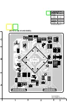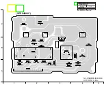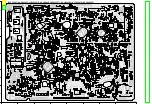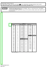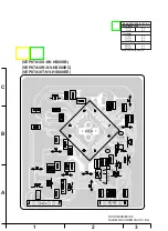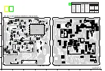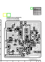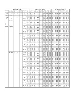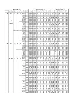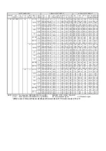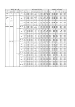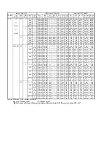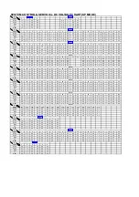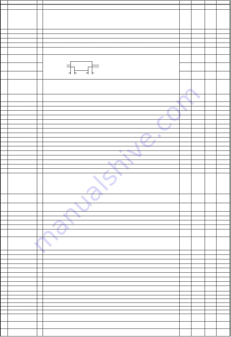
37 V EE(L)
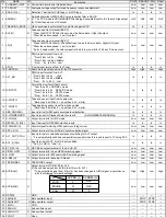
O Output terminal of EE and VV switching.
Low
Low
Low
Low
38 ILLUMI LED ON(H) O
Front Illumination LED ON/OFF control terminal.
* The output is decided according to ON/OFF setting of OSD menu and power ON/OFF
condition of VCR.
* During OSD menu is OFF: Low output
* During OSD menu is ON: VCR power is ON: High output
Low
Low
Low
Low
39 D.A.REC(H)
O Timing control terminal for linear audio recording current.
Low
Low
Low
Low
40 BIAS(L)
O Bias oscillation control terminal for linear audio.
High
Hi-Z
Hi-Z
High
41 FM.MUTE(H)
O Output terminal for audio mute control.
High
High
Low
High
42 FULL ERASE(L)
O Full Erase Head oscillation control terminal.
Low
Low
Low
Low
43 POWER_KEY
I
Input terminal for power on/off command through power button.
(The power on/off is switched by detecting falling edge of H to L.)
In
In
In
In
44 POS.SW3
I
In
In
In
In
45 POS.SW2
I
In
In
In
In
46 POS.SW1
I
In
In
In
In
47 POWER OFF(H)
O
Control signal for power circuit.
*High is existed when turning off the power supply for concerned circuit.
*Low is existed while power is supplied to mechanism and/or concerned circuit, although it
seems to be power off.
High
High
Low
High
48 FIP(L)
O
Control terminal for FIP on/off.
*Low is existed when FIP OFF is selected on the Menu screen and the VCR turns off.
Not fix
High
Low
Low
49 P50 IN
I Interrupt serial input terminal for project 50.
In
In
In
In
50 LC.OSC IN
I Oscillation output terminal for OSD dot clock.
---
---
---
---
51 LC.OSC OUT
O Oscillation input terminal for OSD dot clock.
---
---
---
---
52 RESET(L)
Reset input terminal of microprocessor.
In
In
In
In
53 4FC.LPF
I 4FSC input terminal.
---
---
---
---
54 OSD.FSC IN
I FSC input tewrminal.
---
---
---
---
55 5V(OSD)
Power supply terminal for OSD circuit.
---
---
---
---
56 CVIN
Input terminal for composite video signal.
---
---
---
---
57 GND(OSD)
GND terminal for composite video signal.
---
---
---
---
58 LECHA
I
I
I
I
I
I
I
I
Input terminal for white level of composite video signal.
---
---
---
---
59 20M.START(H)
Control terminal for high/low-speed mode.
---
---
---
---
60 MD0
Mode switching terminal for Overwriting the Flash memory.
---
---
---
---
61 CVOUT
O Output terminal for CG video.
---
---
---
---
62 HLF
O LPF connecting terminal of the Slicer for OSD dot clock.
---
---
---
---
63 VHOLD
O Capacitor connecting terminal of the Slicer for OSD dot clock.
---
---
---
---
64 CVIN(EDS)
Input terminal of the composite video signal for the Slicer.
In
In
In
In
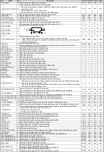
65 SHORT_DN
I
Emergency detection terminal of oscillating circuit for recording.
*The power is turned off Compulsory when this input becomes high while BIAS(L) existing
(The self test indication displays : F08).
*The power is turned off Compulsory when this input becomes Low while BIAS(H) existing
(The self test indication displays : F07).
In
In
In
In
66 UNLOADING(H)
O
Control terminal for Loading motor.(Forward)
*High is existed when the loading motor rotates reverse direction and/or breaking.
Low
Low
Low
Low
67 LOADING(H)
O
Control terminal for Loading motor.(Reverse)
*High is existed when the loading motor rotates forward direction and/or breaking.
Low
Low
Low
Low
68 PAL-I/BG/DK(SYS4) O Output terminal for broad cast system to control the video circuit.
Not fix
Low
Low
Low
69 SECAM/PAL(SYS2) O Output terminal for the unit recognition result of broad cast system.
Low
Low
Low
Low
70 ADD-V
I V-sync. Input terminal.
In
In
In
71 OSD PULSE
O Terminal for abstracting the BOX from Video signal in superimpose mode.
Low
Low
Low
Low
72 SLEEP(L)
O
Output terminal of control signal for super power save mode, to be supplied to power circuit.
*Low is existed when the super power save ON is selected and the unit is in the P-OFF
High
Low
Low
High
73 PROG ON
O
I/O control to switch IIC bus for LW-programmer.
H:IIC bus is connected to AV2.
L:IIC bus is not connected to AV2.
Low
Low
Low
Low
74 NAVI(H)
O NAVI data writing control signal in Vertical Branking Period.
Low
Low
Low
Low
75 NAVI DATA
O NAVI data writing control signal in Vertical Branking Period.
Low
Low
Low
Low
76 P FAIL
I Interrupt input terminal for power fail detection.
In
In
In
In
In
77 IR
I Interrupt input terminal receiving from IR-Remote Controller.
In
In
In
In
78 P50 OUT
O Data output terminal for Project 50 (Q-Link, etc.)
Not fix
Low
Low
Low
79 CAP.ET
O Output terminal for Capstan Torque command.
0V
0V
Low
0V
80 CYL.ET
O Output terminal for Cylinder Torque command.
4.213V 4.213V
Low
4.213V
81 B/W(H)
O B/W mode output terminal.
Low
Low
Low
Low
82 HALF_WAVE(H)
O Control terminal for switching capstan motor speed full-wave (First) and Half-wave mode.
In
In
In
In
83 CAP.R/F
O Capstan motor rotation direction control terminal.
Low
Low
Low
Low
84 125Hz
O Output terminal of the reference 125Hz clock using for clock adjustment.
Not fix
Low
Low
Low
85 FLD/S-BUS CS
O FLD/Slicer bus chip select terminal.
Not fix
Low
Low
Low
86 FLD/S-BUS/T2 CLK O FLD / Slicer bus / Test 2 clock terminal.
Not fix
Low
Low
Low
87 FLD/S-BUS/T2 IN
I FLD/Slicer bus / TEST2 Data output terminal.
Not fix
In
In
In
88 FLD/S-BUS/T2 OUT O FLD/Slicer bus / TEST2 Data in terminal
Not fix
Low
Low
Low
89 5P CLK
O
FIP driver / TEST2 Serial Clock terminal
(Serial clock signal for FIP driver and factory machine)
Not fix
Low
Low
Low
90 5P DATA IN
I
FIP driver / TEST2 Serial data input terminal
(Serial data input signal for FIP driver and factory machine)
Not fix
In
In
In
91 5P DATA OUT
O
FIP driver / TEST2 Serial data output terminal
(Serial data output signal for FIP driver and factory machine)
Not fix
Low
Low
Low
Input terminal for mechanism
140mS
D.A. REC(H)
BIAS(L)
140mS
position.
No.
NAME
I/O
Description
P-OFF P-SAVE P-FAIL
Reset
Summary of Contents for NV-HS880EG
Page 16: ...4 REMOVAL OF THE MAIN C B A Remove Screw F Remove 4 Screws G Unlock 2 Tabs H Fig D5 16 ...
Page 23: ...3 3 8 CIRCUIT BOARD LAYOUT 23 ...
Page 26: ...10 2 CASING PARTS SECTION 26 ...
Page 27: ...10 3 PACKING PARTS SECTION 27 ...
Page 28: ...11 REPLACEMENT PARTS LIST 11 1 CHASSIS PARTS SECTION PARTS LIST 28 ...
Page 41: ...D7501 MAZ4220NMF DIODE MAVD 41 ...
Page 43: ...K7301 ERJ6GEY0R00V M RESISTOR CH 1 10W 0 D0GBR00JA017 43 ...
Page 46: ...Q1104 2SD1992A R TRANSISTOR 46 ...
Page 48: ...R0715 ERJ3GEYJ223 M RESISTOR CH 1 16W 22K 48 ...


