background image

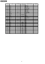
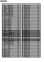
Pin

No.

I/O Setting

Pull-up

Processing

Contents of Control

Remark

30

DVRL

in

-

Comp. Ref.

31

DDR

in

-

Comp. Input

32

DVRH

in

-

Comp. Ref.

33

DDX0

out

-

Tx DATA OUT0

34

DDX1

tri

-

Tx DATA OUT1

35

PVRL

in

-

Comp. Ref.

36

PDR

in

-

Comp. Input

37

PVRH

in

-

Comp. Ref.

38

PDX0

out

-

Tx DATA OUT0

39

PDX1

out

-

Tx DATA OUT1

40

MMODE

in

-

Mode

41

SCAN

in

Pull Down

scan

42

RSTN

in

-

Reset

43

SCANE

in

Pull Down

scan test

44

VDD

-

-

Vdd

45

CK8_16

tri

-

8MHz clock out

46

VSS

-

-

GND

47

OSI

in

-

OSC

48

OSO

out

-

OSC

49

VSS

-

-

GND

50

ADR5

in

Built-in

Add.5

51

ADR4

in

Built-in

Add.4

52

ADR3

in

Built-in

Add.3

53

ADR2

in

Built-in

Add.2

54

ADR1

in

Built-in

Add.1

55

ADR0

in

Built-in

Add.0

56

VDD

-

-

Vdd

57

DB7

bi

Built-in

Data 7

58

DB6

bi

Built-in

Data 6

59

DB5

bi

Built-in

Data 5

60

DB4

bi

Built-in

Data 4

61

DB3

bi

Built-in

Data 3

62

DB2

bi

Built-in

Data 2

63

DB1

bi

Built-in

Data 1

64

DB0

bi

Built-in

Data 0

24

KX-T7665AL / KX-T7665X

Summary of Contents for KX-T7665AL

Page 1: ...RMATION ABOUT LEAD FREE PbF SOLDERING If lead free solder was used in the manufacture of this product the printed circuit boards will be marked PbF Standard leaded Pb solder can be used as usual on boards without the PbF mark When this mark does appear please read and follow the special instructions described in this manual on the use of PbF and how it might be permissible to use Pb solder during ...

Page 2: ...RCUIT OPERATIONS 15 10 1 KEY INPUT CONTROL CIRCUIT 15 10 2 LCD CONTROL CIRCUIT 16 10 3 LED CIRCUIT 17 10 4 RESET CIRCUIT 18 10 5 POWER SUPPLY CIRCUIT 18 10 6 DATA COMMUNICATION 19 10 7 DXDP COMMUNICATION 20 10 8 ANALOG CIRCUIT 21 11 IC DATA 23 11 1 IC2 23 11 2 IC6 25 12 TERMINAL GUIDE OF ICs TRANSISTORS AND DIODES 26 13 CABINET AND ELECTRICAL PARTS LOCATION 27 14 ACCESSORIES AND PACKING MATERIALS ...

Page 3: ...eful not to heat too long PbF solder will tend to splash if it is heated much higher than its melting point approximately 1100 F 600 C If you must use Pb solder on a PCB manufactured using PbF solder remove as much of the original PbF solder as possible and be sure that any remaining is melted prior to applying the Pb solder When applying PbF solder to double layered boards please check the compon...

Page 4: ...49 64 16 C607 C606 10 1 CN5 R601 C602 R602 R604 R603 R600 C601 C600 E4 IC8 D5V R607 IC5 R609 R608 C609 E3 JK2 R T G1 R610 33 48 1 17 32 49 64 1 CN3 R W 2 1 CN2 R200 C205 PSUP1439Z A PbF F5 F7 A5 B1 B2 B3 R135 C120 D3V Q5 Q3 Q6 R139 R138 R133 R137 C204 R JK3 AG1 SP1 SPN SPP Q52 Q51 R504 IC4 IC3 Q23 C203 R206 R209 IC1 R208 R204 Q4 Q22 R207 Q21 C201 R202 L21 C504 C518 R514 R511 C528 R513 R518 MIC2 AG...

Page 5: ...d the soldering irons 3 Use a conductive mat on the worktable 4 Do not touch IC or LSI pins with bare fingers 3 SPECIFICATIONS Station Loop Limit 90 ohms Calling Method 2 pair wire Jacks Handset Jack TEL Jack Dimensions Low Angle High Angle 213 D mm 177 W mm 107 H mm 201 D mm 177 W mm 127 H mm Weight 0 7 kg Design and specifications are subject to change without notice 4 LOCATION OF CONTROLS 5 KX ...

Page 6: ...5 CONNECTION Caution The availability of D XDP function depends on the software version of the connected Business Telephone System Consult your dealer for more details about D XDP 6 KX T7665AL KX T7665X ...

Page 7: ...TRUCTIONS 1 Remove the Stand 2 Remove 5 Screws A 3 Remove the Cabinet Cover 4 Remove the Connector from the Main Board 5 Remove 2 Screws A 6 Remove the Main Board and the LCD from the Cabinet Body 7 KX T7665AL KX T7665X ...

Page 8: ... temporarily soldering two diagonally opposite pins in the correct positions on the PCB Be certain each pin is located over the correct pad on the PCB 2 Apply flux to all of the pins on the IC 3 Being careful to not unsolder the tack points slide the soldering iron along the tips of the pins while feeding enough solder to the tip so that it flows under the pins as they are heated 7 3 REMOVING SOLD...

Page 9: ...8 TROUBLESHOOTING GUIDE 8 1 NO OPERATION Note Refer to 1 4 of WAVEFORM P 34 for waveform 9 KX T7665AL KX T7665X ...

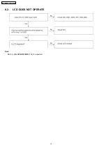
Page 10: ...8 2 LCD DOES NOT OPERATE Note Refer to 5 of WAVEFORM P 34 for waveform 10 KX T7665AL KX T7665X ...

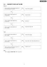
Page 11: ...8 3 HANDSET DOES NOT WORK Receive Send Note Refer to 6 7 of WAVEFORM P 34 for waveform 11 KX T7665AL KX T7665X ...

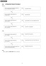
Page 12: ...8 4 SPEAKER PHONE TROUBLE Receive Send Note Refer to 6 7 of WAVEFORM P 34 for waveform 12 KX T7665AL KX T7665X ...

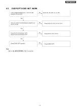
Page 13: ...8 5 DXDP DPT DOES NOT WORK Note Refer to 8 of WAVEFORM P 34 for waveform 13 KX T7665AL KX T7665X ...

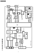
Page 14: ...nication Power IC1 Q21 L21 D3V A3V OSR OSX OEP0 OCK DX DR BCLK FS LED D32 D42 Q31 Q35 NROW0 3 CLM0 5 Key SW1 32 Hook SW JK3 Reset IC7 Speaker Phone IC3 3 3V 5 0V IC8 D63 CODEC IC4 CPU IC6 Tone DB0 7 ADR0 5 WEN REN INTN SCK DATA LCD D4 7 E W RS SCL SDA X1 LED D43 D44 MIC CN2 SP CN1 CN3 CN4 MAIN P C Board KX T7665AL KX T7665X BLOCK DIAGRAM KX T7665AL KX T7665X 14 ...

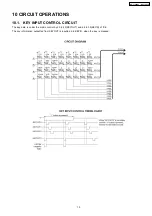
Page 15: ...1 KEY INPUT CONTROL CIRCUIT The key data is under the matrix control by 20 to 23 KEYOUT and 28 to 35 KEYIN of IC6 The key information outputted from KEYOUT is inputted into KEYIN when the key is pressed 15 KX T7665AL KX T7665X ...

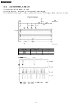
Page 16: ...justment is performed by the circuit composed of R603 and R604 The contrast is determined only by the voltage level between pin 2 and pin 3 of CN5 Higher potential makes the contrast high LCD Contrast Control CONTRAST IC6 Pin 59 IC6 Pin19 HIGH L L MIDDLE Z L LOW Z Z 16 KX T7665AL KX T7665X ...

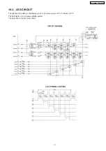
Page 17: ... LED CIRCUIT The lighting of the LED is controlled by pin 14 to 18 Row and pin 8 to 13 Colum of IC2 The LED lights up in a dynamic lighting system The duty ratio is 1 8 ON time 1 5ms 17 KX T7665AL KX T7665X ...

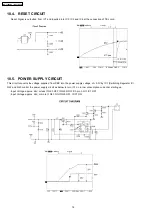
Page 18: ...verts the voltage supplied from PBX into the power supply voltage of 3 3V by IC1 Switching Regulator IC Q22 and Q23 control the power supply circuit as below to turn IC1 on in low consumption current at starting up Input Voltage approx 26V or less Q23 OFF Q22 ON IC1 pin 3 H IC1 OFF Input Voltage approx 26V or more Q23 ON Q22 OFF IC1 ON 18 KX T7665AL KX T7665X ...

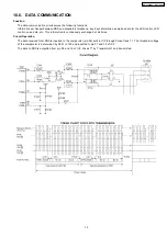
Page 19: ...trol voice data etc This information is continuously exchanged at all times Circuit Operation The data received from PBX is inputted to the comparator pin 36 built in IC2 through Pulse Trans T1 The threshold voltage of the comparator is determined by R101 to 103 and inputted to pin 37 and 35 of IC2 The data to PBX is outputted from pin 38 and 39 of IC2 drives T1 by Transistor Q1 and transmitted 19...

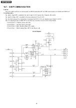
Page 20: ...ve DPT is inputted to the comparator pin 31 built in IC2 The threshold voltage of the comparator is determined by R112 to 114 and inputted to pin 30 and 32 of IC2 Also the supplying power to Slave DPT is controlled by a constant current circuit of Q16 as below IC2 pin 28 as H Constant current circuit ON IC2 pin 28 as L Constant current circuit OFF IC2 pin 29 as H 40mA Feeding Slave DPT usually IC2...

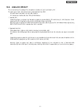
Page 21: ...on after the input to IC4 in PCM data Gain adjustment by DSP of IC4 Pin 26 of IC4 outputted from Q51 to handset 2 Speakerphone Call The speakerphone mode can only provide a one way communication path IC3 compares transmitting signal and receiving signal during speakerphone mode then provide a one way communication path Transmitting signal is inputted from SP phone mic and amplified by IC4 built in...

Page 22: ...0 FS 7 HANDR 26 TONE 30 MIC1 17 CSN 13 DATA 11 RAO 28 SPI 29 TEST 14 C515 C514 R512 R511 C506 C524 R505 R506 A3V AG AG C521 IC3 FS 2 TIN 4 RIN 3 VDD 7 VSS 8 TOUT 6 ROUT 5 DATA 11 SCLK 13 CSN 14 TEST1 15 RxON 9 TxON 10 RST 16 TEST2 12 BCLK 1 C522 D3V R515 D3V C525 R503 AG Q51 E C B AG AG NC C503 MIC1 SP1 AG1 SPP SPN MIC2 AG2 R406 D3V R518 R519 R520 R521 DG R516 DG R517 DG DG DG C523 DG R514 R513 AG...

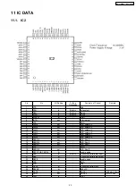
Page 23: ...11 CLM2 out LED column 2 12 CLM1 out LED column 1 13 CLM0 out LED column 0 14 NROW3 out LED Row 3 15 NROW2 out LED Row 2 16 NROW1 out LED Row 1 17 VSS GND 18 NROW0 out LED Row 0 19 OEP1 PN9 CK512K tri enable pulse 20 OSR in Built in 2 048MHz serial data input 21 OSX tri 2 048MHz serial data output 22 OEP0 tri enable pulse 23 VSS GND 24 VDD Vdd 25 OCLK bi 2 048MHz serial clock 26 OSYNC bi 8Khz FS 2...

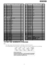
Page 24: ...RSTN in Reset 43 SCANE in Pull Down scan test 44 VDD Vdd 45 CK8_16 tri 8MHz clock out 46 VSS GND 47 OSI in OSC 48 OSO out OSC 49 VSS GND 50 ADR5 in Built in Add 5 51 ADR4 in Built in Add 4 52 ADR3 in Built in Add 3 53 ADR2 in Built in Add 2 54 ADR1 in Built in Add 1 55 ADR0 in Built in Add 0 56 VDD Vdd 57 DB7 bi Built in Data 7 58 DB6 bi Built in Data 6 59 DB5 bi Built in Data 5 60 DB4 bi Built in...

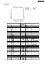
Page 25: ...L Cont L High Z 20 P14 I O Built in KEYOUT3 L output 21 P13 TMIG I O Built in KEYOUT2 L output 22 P12 TMOFH I O Built in KEYOUT1 L output 23 P11 TMOFL I O Built in KEYOUT0 L output 24 P10 TMOW O OSC for LCD Power 128kHz 4 096MHz 32 25 PA3 O side tone Cont H side tone ON 26 PA2 O ASIC REN Low active 27 PA1 O ASIC WEN Low active 28 P50 WKP0 I Built in KEYIN0 29 P51 WKP1 I Built in KEYIN1 30 P52 WKP2...

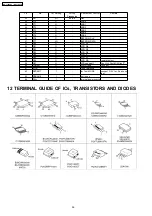
Page 26: ... 52 P80 O LCD_D7 53 P81 O LCD_D6 54 P82 O LCD_D5 55 P83 O LCD_D4 56 P84 O LCD_E 57 P85 O LCD_W 58 P86 O LCD_RS register select 59 P87 O LCD contrast 1 Cont H L Cont M L High Z 60 TONED O DTMF Tone Tone out 61 VTref I Tone reference 62 PB7 AN7 I for Test MODE connect D3V for Sp phone test 63 PB6 AN6 I not in use 64 CVcc I internal power source 12 TERMINAL GUIDE OF ICs TRANSISTORS AND DIODES 26 KX T...

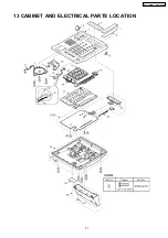
Page 27: ...13 CABINET AND ELECTRICAL PARTS LOCATION 27 KX T7665AL KX T7665X ...

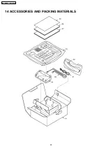
Page 28: ...14 ACCESSORIES AND PACKING MATERIALS 28 KX T7665AL KX T7665X ...

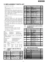
Page 29: ...ption Remarks 7 PQAS57P03Z SPEAKER 8 PSJS02P15Z CONNECTOR 2 PIN 9 PSUS1026Z TORSION SPRING 10 PSBH1007Z1 PUSH BUTTON HOOK PC ABS HB S 11 PSHG1122Z RUBBER PARTS MIC COVER 12 RJM142Z BUILTIN MICROPHONE S 13 PSJS02Q35Y CONNECTOR 2 PIN 14 PSBX1116Z1 PUSH BUTTON FUNCTION ABS HB S 15 PSBX1089Z1 PUSH BUTTON 12 KEY ABS HB S 16 PSBX1117Z1 PUSH BUTTON CO LINE ABS HB S 17 PSSX1030Z1 KEYBOARD SWITCH S 18 PSJS...

Page 30: ...3 12K R104 ERJ3GEYJ182 1 8K R105 ERJ3GEYJ122 1 2K R106 ERJ3GEYJ121 120 R107 ERJ3GEYJ182 1 8K R108 ERJ3GEYJ101 100 R109 ERJ3GEYJ101 100 R110 ERJ3GEYJ122 1 2K R111 ERJ3GEYJ122 1 2K Ref No Part No Part Name Description Remarks R112 ERJ3GEYJ562 5 6K R113 ERJ3GEYJ682 6 8K R114 ERJ3GEYJ103 10K R115 ERJ3GEYJ472 4 7K R116 ERJ3GEYJ153 15K R117 ERJ3GEYJ472 4 7K R119 ERJ3GEYJ822 8 2K R129 ERJ3GEYJ123 12K R13...

Page 31: ...escription Remarks C403 ECUV1C104ZFV 0 1 C404 ECUV1H120JCV 12P C405 ECUV1H120JCV 12P C406 ECUV1H120JCV 12P C407 ECUV1C104ZFV 0 1 C500 ECUV1H222KBV 0 0022 C501 ECUV1H102KBV 0 001 C502 ECUV1C104KBV 0 1 C504 ECUV1E103KBV 0 01 C506 ECUV1H333KBV 0 033 S C507 ECUV1H152KBV 0 0015 C508 ECUV1C104KBV 0 1 C509 ECUV1H152KBV 0 0015 C510 ECUV1H223KBV 0 022 S C511 ECUV1C104KBV 0 1 C512 ECUV1E103KBV 0 01 C513 ECU...

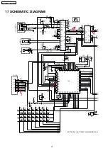
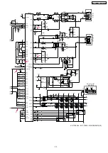
Page 32: ...10 C525 R503 1K AG Q51 E C B AG AG NC C503 D63 D62 D3V Z0 1 C604 D5V IC7 NC 3 Vss 4 Vin 2 Vout 1 SW33 MIC1 SP1 AG1 SPP SPN MIC2 AG2 IC6 64 CVcc 63 PB6 62 PB7 61 VTref 60 TONED 59 P87 58 P86 57 P85 56 P84 55 P83 54 P82 53 P81 52 P80 51 P77 50 P76 49 P75 48 P74 47 P73 46 P72 45 P71 44 P70 43 P67 42 P66 41 P65 40 P64 39 P63 38 P62 37 P61 36 P60 35 P57 34 P56 33 P55 17 P17 18 P16 19 P15 20 P14 21 P13 ...

Page 33: ...O2 D39 CO6 D38 CO5 4 3 5 120 R309 4 3 5 D37 CO4 D35 CO8 A1 4 3 5 D32 CO1 12 R308 120 R307 D33 CO7 D42 STORE DG D3V R515 47K D3V Z0 1 C403 D3V Z0 1 C402 Z0 1 C401 Z0 1 C400 R401 1M R400 820 X1 16 384MHz 12P C404 12P C405 Z0 1 C407 JK1 1 H 2 R 3 T 4 L R204 3 9k 1k R300 1k R304 1k R301 1k R305 1k R302 1k R303 D31 SP 120 R310 180 R306 CN3 1 2 B6 B1 B4 B5 B3 B2 CN4 2 1 4 7 R313 D41 INTERCOM B7B8 B9B10 ...

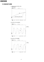
Page 34: ...18 WAVEFORM 2 3 1 Pin48 of IC2 16 384MHz Pin45 of IC2 8 196MHz Pin42 of IC2 and Pin8 of IC6 Rest signal Pin42 of IC2 and Pin8 of IC6 34 KX T7665AL KX T7665X ...

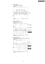
Page 35: ... 5 6 4 Pin4 to 7 of CN5 Communication waveform Pin3 and 6 of IC3 PCM interface waveform between IC3 and IC2 Pin36 of IC2 Communication waveform 35 KX T7665AL KX T7665X ...

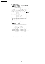
Page 36: ... 8 7 Pin31 of IC2 Communication waveform Pin8 and 10 of IC4 PCM interface waveform between IC4 and IC3 36 KX T7665AL KX T7665X ...

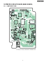
Page 37: ...2 R604 R603 R600 C601 C600 E4 IC8 D5V R607 IC5 R609 R608 C609 E3 JK2 R T G1 R610 33 48 1 17 32 49 64 1 CN3 R W 2 1 CN2 R200 C205 PSUP1439Z A 2 CN4 R312 B8 B9 B7 B10 R313 1 PbF F5 F7 A5 B1 B2 B3 R135 C120 D3V Q5 Q3 Q6 R139 R138 R133 R137 C204 R R W JK3 AG1 SP1 SPN SPP Q52 Q51 R504 IC4 IC3 Q23 C203 R206 R209 IC1 R208 R204 Q4 Q22 R207 Q21 C201 R202 L21 C504 C518 R514 R511 C528 R513 R518 MIC2 AG2 GND ...

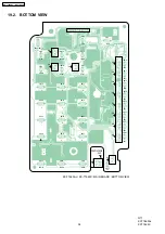
Page 38: ... SW17 CO3 SW21 CO2 SW25 CO1 SW4 V DWN SW16 1 SW20 4 SW24 7 SW28 REDIAL SW32 FLASH SW30 HOLD SW31 SP SW29 PSUP1439Z B PbF HOOK SW SW15 2 SW19 5 SW23 8 SW27 0 SW14 3 SW3 MES SW18 6 SW22 9 SW26 D40 D42 D35 D33 D39 D38 D37 D36 D34 D32 D31 D44 D43 KX T7665AL KX T7665X MAIN BOARD BOTTOM VIEW 38 KX T7665AL KX T7665X NT1 KXT7665AL KXT7665X ...

Reviews: