background image

2.2.

 Digital

Block

Diagram

Change

from

origina

l

page

63

(2.3.3.4

.1.

Digital

Block

Diagra

m

)

IC501

ASIC

ADR[15:13]

RBA[6:0]

ADR[12:0]

DB[7:0]

XRD

XWR

XROMCS

XRAMCS

XMDMCS

IC502

ROM

IC504

SRAM

IC505
MODEM

A[17:0]

D[7:0]

XRD

XCS

A[16:0]

D[7:0]

XRD

XWR

XCS

A[4:0]

D[7:0]

XRD

XWR

XCS

XWDERR

IN

OUT

GND

+5V

+3.3V

TO
OP-PANEL

KSTART,KLATCH
KSCLK,KTXD

KRXD,JOG1,JOG2

TO
CIS

F1,FTG
CISLEDON

VIDEO

TO
THRMAL
HEAD

THDAT,THCLK,THLAT
STB1,STB2,STB3

TM

+24V

TO
MOTOR

TM[3:0],TXE

TO
POWER
SUPPLY

+24V,+5V,PG,DG

OP-RESET

+24V

PDET

XRESETI

XORESET

XRESET

XBACKEN

RESET-

IC

+3V/BATT

+5V/BATT

VCC

BATT

+

-

24MHz

32.768KHz

TX

RX

TO
ANALOG
PCB

SP-AMP

TO
SPEAKER

A[12:0]

RBA[5:0]

A[11:0]

RBA[2:0]

A[4:0]

+5V

XRAS

XCAS

A[9:0]

D[7:0]

XRD

XWR

XRAS

XCAS

IC503

DRAM

A[7:4]

RBA[5:0]

FILMEND

PAPER
TOP

SENSOR
LED ON

PS501

32.256MHz

TO
POSITIO
N
SW

+5V

CN505

CN504

CN508

CN507

CN506

CN509

PS501

CN503

B

A

G

DIR

IC550

CN501,502

MIDATA

MICLK

MILAT

IC551

ANALOG ASIC

You

also

need

to
check

the

signal

lines

listed

here

[List

1]
when

the

unit

fails

to
boot

up

the

system

.

Those

signal

lines

should

remain

normal

.

Other

signal

lines

are

not

directly

related

to

that

failure

even

if

they

have

faults

or
trouble

s

.

12

KX-

FP105

RS

Summary of Contents for KX-FP105RS

Page 1: ...on is a violation of law KX FP105RS for Russia Compact Plain Paper FAX Please file and use this manual together with the service manual for Model No KX FP101AL Order No KM79909316C3 This Service Manual indicates the main differences between Original KX FP101AL and KX FP105RS ORDER NO KMF0002387A3 ...

Page 2: ...3 times Bottom View 1 2 PERSONAL SAFETY PRECAUTIONS 1 2 1 LIVE ELECTRICAL SECTIONS Change from original page 4 1 6 2 LIVE ELECTRICAL SECTIONS All the electrical sections of the unit supplied with AC power by the AC power cord are live Never disassemble the unit for service with the AC power supply plugged in CAUTION AC voltage is supplied to the primary side of the power supply unit Therefore alwa...

Page 3: ...on Remote FAX receiving using an extension phone 150 sheet paper capacity Automatic fax phone switching Distinctive ring detection The 12 second speed is based upon the ITU T Test Chart on the condition that memory transmission is performed Subscription to distinctive ring services required Large Memory 28 pages Performed by DRAM Approx 28 pages of memory reception Approx 25 pages of memory transm...

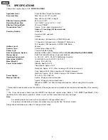
Page 4: ...imensions H W D 143 325 305 mm 5 5 8 12 13 16 12 Mass Weight Approx 4 0 kg 8 8 lb Power Consumption Standby Approx 6 5 W Transmission Approx 15 W Reception Approx 42 W When receiving a 20 black document Copy Approx 45 W When copying a 20 black document Maximum Approx 150 W When copying a 100 black document Power Supply 220 240 V AC 50 60 Hz Memory Capacity Approx 28 pages memory reception Approx 2...

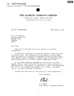
Page 5: ...1 5 CCITT Test Chart Change from original page 8 1 11 ITU T Test Chart Actual size 5 KX FP105RS ...

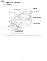
Page 6: ...TION OF CONTROLS 1 6 1 OVERVIEW Change from original page 9 1 12 1 OVERVIEW Note The document and recording paper will be ejected from the front of the unit Do not put anything in front of the unit 6 KX FP105RS ...

Page 7: ...1 6 2 CONTROL PANEL Change from original page 10 1 12 2 CONTROL PANEL 7 KX FP105RS ...

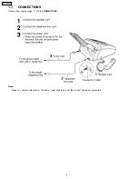
Page 8: ...1 7 CONNECTIONS Change from original page 11 1 13 CONNECTIONS Note When you operate this product the power outlet should be near the product and easily accessible 8 KX FP105RS ...

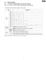
Page 9: ...ATION 1 8 1 TO SELECT CHARACTERS WITH THE DIAL KEYPAD Change from original page 18 1 14 10 TO SELECT CHRACTERS WITH THE DIAL KEYPAD Note A hyphen entered in a telephone number is counted as two digits 9 KX FP105RS ...

Page 10: ... ON OK 077 Auto answer mode 1 FAX Only 2 TEL FAX FAX Only OK 078 TEL FAX ring 1 to 4 rings 1 OK 079 Film detection 1 ON 2 OFF ON OK 080 Set default YES NO NO NG 501 Pause time set 001 600 x 100msec 050 OK 502 Flash time 01 99 x 10msec 070 OK 503 Dial speed 1 10pps 2 20 pps 10pps OK 511 Vox sense 1 HIGH 2 LOW HIGH OK 520 CED frequency select 1 2100Hz 2 1100Hz 2100 OK 521 International mode select 1...

Page 11: ... feed 1 ON 2 OFF ON OK 763 CNG detect time for friendly reception 1 10s 2 20s 3 30s 30s OK 771 T1 timer 1 35s 2 60s 35s OK 774 T4 Timer 00 99 X100ms 00 OK 815 Sensor VOX test NG 852 Print test pattern NG 853 Top margin 1 9 OK 854 Left margin 1 8 OK 861 A4 size set 1 ON 2 OFF ON OK 880 History list 1 Start NG 890 TEL FAX ring back tone 1 ON 2 OFF ON OK 991 Setup list 1 Start OK 994 Journal list 1 S...

Page 12: ...DG OP RESET 24V PDET XRESETI XORESET XRESET XBACKEN RESET IC 3V BATT 5V BATT VCC BATT 24MHz 32 768KHz TX RX TO ANALOG PCB SP AMP TO SPEAKER A 12 0 RBA 5 0 A 11 0 RBA 2 0 A 4 0 5V XRAS XCAS A 9 0 D 7 0 XRD XWR XRAS XCAS IC503 DRAM A 7 4 RBA 5 0 FILMEND PAPER TOP SENSOR LED ON PS501 32 256MHz TO POSITIO N SW 5V CN505 CN504 CN508 CN507 CN506 CN509 PS501 CN503 B A G DIR IC550 CN501 502 MIDATA MICLK MI...

Page 13: ...gins at the handset microphone and the signal is output to the telephone line The signal mainly flowing on this route is analog You can trace the signal with an oscilloscope The signal flow on each route is shown in the Check Sheet here If you find a specific problem in the unit for example if you cannot communicate with the H S trace that signal route locally with the following Check Sheet and lo...

Page 14: ...ears on each route between the handset microphone and telephone line sending or between the telephone line and the handset speaker receiving or between the telephone line and the speaker monitor Check the components at that point CHECK SHEET in 2 3 3 5 Analog Board Section is useful for this investigation b No pulse dialing c No ring tone or No bell d No tone dialing 14 KX FP105RS ...

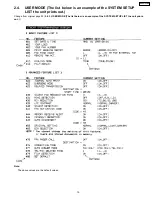
Page 15: ...an example of the SYSTEM SETUP LIST the unit prints out Change from original page 83 2 4 3 USER MODE The list below is an example of the SYSTEM SETUP LIST the unit prints out Note The above values are the default values 15 KX FP105RS ...

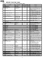
Page 16: ... 1 ON 2 OFF 1 2 1 See 2 2 1 Paper Jam 561 KEY test See 2 5 TEST FUNCTIONS 570 BREAK select 1 61 2 67 1 2 1 Sets the break of pulse dialing according PBX 571 ITS auto redial time set X number of times 00 99 14 Selects the number of times that ITS is redialed not including the first dial 572 ITS auto redial line disconnection time set X second 001 999 30 Sets the interval of ITS redialing 573 Remote...

Page 17: ...eed 1 ON 2 OFF 1 2 1 When the power is turned on the film is wound to take up any slack 763 CNG detect time for friendly reception 1 10 sec 2 20 sec 3 30 sec 1 3 3 Selects the CNG detection tome of friendly reception 771 T1 timer 1 35 sec 2 60 sec 1 2 1 Sets a higher value when the response from the other party needs more time during FAX transmission 774 T4 Timer 00 99 X100 msec 00 99 0 Use this f...

Page 18: ...2 6 SERVICE MODE SETTINGS Example of a printed out list Change from original page 86 2 4 5 SERVICE MODE SETTINGS Example of a printed out list Note The above values are the default values 18 KX FP105RS ...

Page 19: ...ear and time set by the user after they purchased the unit 10 TIME The shows the very first month date year and time set by the user after they purchased the unit 11 USAGE TIME The amount of time the unit has been powered ON 12 FACTORY NOW This shows how many days from factory production until the user prints out this history list 13 TEL MODE The amount of time the TEL mode setting was used 14 FAX...

Page 20: ...2 8 BUTTON CODE TABLE Change from original page 97 2 5 2 BUTTON CODE TABLE Note These codes 00 01 are only for the data in the History Report 20 KX FP105RS ...

Page 21: ...3 DISASSEMBLY INSTRUCTIONS Change from original pages 109 and 116 4 DISASSEMBLY INSTRUCTIONS 21 KX FP105RS ...

Page 22: ...22 KX FP105RS ...

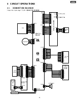
Page 23: ...DG 5V 1 2 3 4 5 6 7 8 1 2 3 4 5 6 7 8 10 11 OPERATION BOARD 1 2 3 4 5 6 7 8 9 RESET 11 CN102 CN502 DG 1 AG 2 5VA 3 5VD 4 24V 5 HSRX 6 7 HSTX 8 9 1 2 3 4 5 6 7 8 1 24V 2 24V 3 GND 4 GND 5 5V 6 THER 7 STB1 8 STB2 9 STB3 10 THCLK 11 THLAT 12 THDAT 9 CN101 CN501 BELL 1 2 3 4 P SHORT 5 LINE RLY 6 BREAK 7 LINE RX 8 ANALOG BOARD HAND SET CN105 HSMIC HSSP 4 3 HSSP HSMIC 2 1 THERMAL HEAD MOD RX 9 LINE TX 1...

Page 24: ...05 HS MIC HS SP HS SP HS MIC 3 3V 5V 24V 3V BATT TXM CN506 MOTOR SPEAKER CPU RTC OSC IC503 IC501 IC505 IC502 IC504 IC551 ANALOG P C B CN508 CN504 CN503 FILM END THERMAL HEAD DRAM ROM X POINT SRAM 5V BATT RECTIFIER DC DC CONVERTER SWITCHING POWER SUPPLY AC NOISE FILTER CN505 4Mbit 4Mbit 256kbit MODEM VOL IN VOL OUT RX TX TONE 1 HS TX LINETX MDNRX CN103 CN104 T T1 R R1 LINERX HS RX 12MHz 24MHz 32 25...

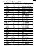
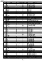
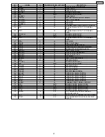
Page 25: ...V POWER SOURCE 5V 26 VSS GND POWER SOURCE GND 27 RVN I 5V INPUT PORT FILM END SENSOR SIGNAL 28 IRDATXD IOP O 5V OUTPUT PORT RESERVED 29 IRDARXD IOP80 I 5V OUTPUT PORT RESERVED 30 TXD IOP O 5V OUTPUT PORT RESERVED 31 RXD IOP O 5V OUTPUT PORT RESERVED 32 XRTS IOP O 5V OUTPUT PORT RESERVED 33 XCTS IOP O 5V OUTPUT PORT RESERVED 34 XDSR IOP O 5V OUTPUT PORT RESERVED 35 DCD IOP O 5V OUTPUT PORT RESERVED...

Page 26: ...UTPUT PORT CSBR 94 DB3 I O 5V CPU DATA BUS 3 95 DB2 I O 5V CPU DATA BUS 2 96 DB4 I O 5V CPU DATA BUS 4 97 DB1 I O 5V CPU DATA BUS 1 98 DB5 I O 5V CPU DATA BUS 5 99 DB0 I O 5V CPU DATA BUS 0 100 DB6 I O 5V CPU DATA BUS 6 101 DB7 I O 5V CPU DATA BUS 7 102 VSS GND POWER SOURCE GND 103 VDD 5V 5V POWER SOURCE 5V 104 XROMCS I O 5V ROM IC502 CHIP SELECT 105 RD O 5V CPU RD 106 WR O 5V CPU WR 107 ADR0 O 5V...

Page 27: ...OUTPUT FOR DATA LATCH 152 RM0 IOP I 5V INPUT PORT P TOP 153 RM1 IOP I 5V OUTPUT PORT RESERVED 154 RM2 IOP I 5V OUTPUT PORT CPC 155 RM3 IOP O 5V NOT USED 156 RXE IOP I 5V INPUT PORT NOT USED 157 TMO O 5V MOTOR A PHASE 158 VDD 5V 5V POWER SOURCE 5V 159 VSS GND POWER SOURCE GND 160 TM1 IOP O 5V MOTOR B PHASE 161 TM2 IOP O 5V MOTOR A PHASE 162 TM3 IOP O 5V MOTOR B PHASE 163 TXE IOP O 5V MOTOR ENABLE S...

Page 28: ...4 4 ANALOG UNIT BLOCK DIAGRAM Change from original page 160 6 7 1 ANALOG UNIT BLOCK DIAGRAM 28 KX FP105RS ...

Page 29: ...e the signal is amplified to about 21dB Then it is output from pin 1 of IC101 and transmitted to T101 via C133 R219 R125 If the side tone circuit is not applied the transmission signal will return to the reception amplifier via C126 R131 R222 and C229 When the side tone circuit is active the signal output from IC101 pin 1 passes through C133 R221 R216 R127 C123 R223 and goes into the amplifier IC1...

Page 30: ...inal page 166 6 10 OPERATION BOARD SECTION The unit consists of a LCD Liquid crystal display KEYs and LEDs light emitting diodes They are controlled by the Gate Array IC301 and ASIC IC501 on the DIGITAL BOARD Fig a Fig a Key Matrix 30 KX FP105RS ...

Page 31: ...DIAGRAM 5 1 SCHEMATIC DIAGRAM ANALOG BOARD Change from original page 179 11 SCHEMATIC DIAGRAM ANALOG CIRCUIT HANDSET FAX TX HANDSET MONITOR FAX RX FAX TX Signal FAX RX Signal NOT USED NC NO COMPONENT KX FP105RS 31 ...

Page 32: ...5 2 MEMO KX FP105RS 32 ...

Page 33: ...6 CABINET MECHANICAL AND ELECTRICAL PARTS LOCATION 6 1 OPERATION PANEL SECTION Change from original page 191 18 1 OPERATION PANEL SECTION 33 KX FP105RS ...

Page 34: ...6 2 LOWER P C B SECTION Change from original page 194 18 3 LOWER P C B SECTION 34 KX FP105RS ...

Page 35: ...Z SPRING DOCUMENT GUIDE 17 PFDG1002Z GEAR DOCUMENT GUIDE 18 PFKR1013Z1 GUIDE DOCUMENT 19 PFGG1036U1 OPERATION PANEL 20 PFBX1069Z1 BUTTON DIAL 21 PFBX1072Y1 BUTTON IQ FAX 22 PFHX1154Y SHEET HEAD FULCROM 23 PFJS11Q26Z CONNECTOR 11P 24 PFBX1070Z1 BUTTON 8 KEY 25 PFDE1084Y LEVER DOC DETECTION 26 PFBC1032Z1 LEVER AUTO ANSWER 27 PFDE1085Z LEVER 28 PFDE1086Z LEVER COVER OPEN SENSOR 29 PFUS1027Z SPRING DO...

Page 36: ...055Z SPRING ONE WAY 175 PFHX1264Y SPACER ROLLER 176 PFDE1059Z DELAY 177 PFDG1085Z GEAR SEPARATION ROLLER 178 XUC2FY RETAINING RING 179 XWC4B WASHER 180 PFHX1263Z SHEET ROLLING 181 PFHX1246Z COVER SCREW 182 Not Used 183 PFHX1148Z VIBRATION SHEET Ref No Part No Part Name Description Remarks 184 PFHX1272Z SHEET CIS LED 185 PQHM112Z CLAMPER 186 Not Used 187 PFNW1006Z WASHER 188 KR06TT251508 FERRITE CO...

Page 37: ...1ET COIL L502 PQLQR1ET COIL L504 PQLQR2KA113T COIL Ref No Part No Part Name Description Remarks L517 PQLQR2KA20T COIL L518 PQLQR2KA113T COIL CRYSTAL OSCILLATIONS X501 PFVCCFS32Z CRYSTAL OSCILLATOR X502 PQVCJ2400N5Z CRYSTAL OSCILLATOR X503 PFVC32256ZAT CRYSTAL OSCILLATOR COMPONENTS COMBINATIONS RA501 EXRV8V101JV COMPONENTS PARTS RA502 EXRV8V101JV COMPONENTS PARTS RA503 EXRV8V101JV COMPONENTS PARTS ...

Page 38: ...YJ103 10K R684 ERJ3GEYJ103 10K R685 ERJ3GEYJ103 10K R686 ERJ3GEYJ103 10K Ref No Part No Part Name Description Remarks R687 ERJ3GEYJ103 10K R689 ERJ6GEY0R00 0 R690 ERJ3GEYJ101 100 R691 ERJ3GEYJ101 100 R692 ERJ3GEYJ101 100 R693 ERJ3GEY0R00 0 R695 ERJ3GEYJ101 100 R696 ERJ3GEYJ101 100 R697 ERJ3GEYJ154 150K R698 ERJ3GEYJ114 110K R701 ERJ3GEYJ151 150 R702 ERJ3GEYJ392 3 9K R703 ERJ3GEYJ564 560K R704 ERJ3...

Page 39: ...PQCUV1E104MD 0 1 S C649 ECUV1C104KBV 0 1 C651 PQCUV1C224KB 0 22 C652 ECUV1H681JCV 680P C653 ECUV1H681JCV 680P C654 ECUV1H681JCV 680P C655 ECUV1C473KBV 0 047 C656 ECUV1H331JCV 330P S C657 PQCUV1H104ZF 0 1 C658 PQCUV1H104ZF 0 1 C659 ECUV1H104ZFV 0 1 S C660 PQCUV1H105JC 1 S C665 ECUV1H104ZFV 0 1 S C666 ECUV1H104ZFV 0 1 S Ref No Part No Part Name Description Remarks FUSES F501 XBAPF001312 FUSE F502 PF...

Page 40: ...7k S R121 PQ4R10XJ821 820 S Ref No Part No Part Name Description Remarks R123 PQ4R10XJ222 2 2k S R124 PQ4R10XJ303 30k S R125 PQ4R10XJ102 1k S R126 ERJ6GEY0R00 0 R127 PQ4R10XJ563 56k S R128 PQ4R10XJ511 510 S R129 PQ4R10XJ181 180 S R130 PQ4R10XJ104 100k S R131 PQ4R10XJ563 56k S R132 PQ4R10XJ104 100k S R137 PQ4R10XJ333 33k S R138 ERJ6GEYJ364 360k R140 PQ4R10XJ222 2 2k S R145 PQ4R10XJ331 330 S R146 PQ...

Page 41: ...3GEY0R00 0 R307 ERJ3GEYJ181 180 R308 ERJ3GEYJ181 180 R309 ERJ3GEYJ181 180 R310 ERJ3GEY0R00 0 R311 ERJ3GEY0R00 0 R312 ERJ3GEY0R00 0 R313 ERJ3GEY0R00 0 R314 ERJ3GEY0R00 0 R315 ERJ3GEY0R00 0 R316 ERJ3GEY0R00 0 R321 ERJ3GEYJ101 100 R322 ERJ3GEYJ273 27K R323 ERJ3GEYJ101 100 R324 ERJ3GEYJ472 4 7K R326 ERJ3GEYJ102 1K R327 ERJ3GEYJ563 56K R328 ERJ3GEYJ331 330 R330 ERJ3GEYJ331 330 R331 ERJ3GEYJ221 220 R342...

Page 42: ...J823 82K S R104 ERG2DJ204 200K S R105 ERX2SJR22 0 22 R106 ERG1SJ470 47 R107 PQ4R10XJ680 68 S Ref No Part No Part Name Description Remarks R108 ERDS2FJ150 15 R109 ERDS2FJ100 10 R110 ERG2DJ204 200K S R121 PQ4R10XJ103 10K S R122 PQ4R10XJ391 390 S R123 PQ4R10XJ221 220 S R125 PQ4R10XJ103 10K S R126 PQ4R10XJ562 5 6K S R127 PQ4R10XJ182 1 8K S R128 PQ4R10XJ124 120K S R129 PQ4R10XJ124 120K S R130 PQ4R10XJ1...

Page 43: ...TURES AND TOOLS Ref No Part No Part Name Description Remarks EC1 PQZZ2K1Z CONNECTOR 2P EC2 PFZZ5K13Z CONNECTOR 5P EC3 PQZZ12K4Z CONNECTOR 12P EC4 PQZZ2K12Z CONNECTOR 2P EC5 PFZZ11K12Z CONNECTOR 11P EC6 PFZZ10K1Z CONNECTOR 10P EC7 PQZZ8K18Z CONNECTOR 8P EC8 PFZZ9K1Z CONNECTOR 9P EC9 PFZZ10K3Z CONNECTOR 10P EC10 PQZZ2K1Z CONNECTOR 2P KM79811245C0 BASIC FACSIMILE TECHNIQUE for training service techni...

Reviews: