
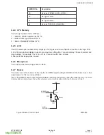

http://cxema.ru
5
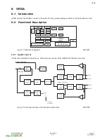
RECEIVER
5.1
Introduction
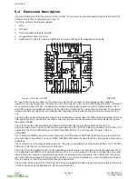
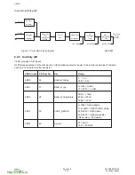
This section provides a technical description of the receiver section of the RF circuit. A circuit diagram of the whole
system is provided in Section 8 of the Service Manual (Order No. MCUK980101C8).
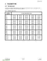
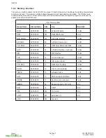
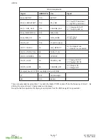
5.1.1 Downlink Frequencies
CHANNEL
NUMBERS
DOWNLINK FREQUENCIES (MHz)
1-5
6-10
11-15
16-20
21-25
935.200
936.200
937.200
938.200
939.200
935.400
936.400
937.400
938.400
939.400
935.600
936.600
937.600
938.600
939.600
935.800
936.800
937.800
938.800
939.800
936.000
937.000
938.000
939.000
940.000
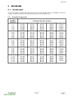
26-30
31-35
36-40
41-45
46-50
940.200
941.200
942.200
943.200
944.200
940.400
941.400
942.400
943.400
944.400
940.600
941.600
942.600
943.600
944.600
940.800
941.800
942.800
943.800
944.800
941.000
942.000
943.000
944.000
945.000
51-55
56-60
61-65
66-70
71-75
945.200
946.200
947.200
948.200
949.200
945.400
946.400
947.400
948.400
949.400
945.600
946.600
947.600
948.600
949.600
945.800
946.800
947.800
948.800
949.800
946.000
947.000
948.000
949.000
950.000
76-80
81-85
86-90
91-95
96-100
950.200
951.200
952.200
953.200
954.200
950.400
951.400
952.400
953.400
954.400
950.600
951.600
952.600
953.600
954.600
950.800
951.800
952.800
953.800
954.800
951.000
952.000
953.000
954.000
955.000
101-105
106-110
111-115
116-120
121-124
955.200
956.200
957.200
958.200
959.200
955.400
956.400
957.400
958.400
959.400
955.600
956.600
957.600
958.600
959.600
955.800
956.800
957.800
958.800
959.800
956.000
957.000
958.000
959.000
MCUK980101G8
Section 5
Issue 1
Technical Guide
5 - 1
Revision 0
RECEIVER