background image

Item

FL display

Key operation

Mode name

Description

(Remote controller key)

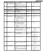
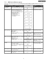
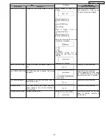
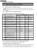
RAM Drive Last Error

RAM Drive error code display.
*For details about the drive error code, refer
to the Service Manual for the specific RAM
Drive.

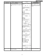
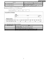
1. Error Number is displayed for 5
seconds.

2. Time when the error has
occurred (1/2) is displayed for 5
seconds.

YY: Year
MM: Month
DD: Day
3. Time when the error has
occurred (2/2) is displayed for 5
seconds.

hh: Hour
mm: Minute
ss: Second
4. Last Drive Error code No.1 is
displayed for 5 seconds.

5. Last Drive Error code No.2 (1/2)
is displayed for 5 seconds.
(This Error Code is unnecessory
for service.)

6. Last Drive Error code No.2 (2/2)
is displayed for 5 seconds.
(This Error Code is unnecessory
for service.)

7. Error occurring Disc type is
displayed for 5 seconds.

DISC 1: DVD
DISC 2: CD
DISC 3: DVD-RAM 2.6GB
DISC 4: DVD-RAM 4.7GB
DISC 5: DVD-R
DISC

: Unknown Disc

8. Unused (No display)

9. Factor of Drive Error occurring is
left displayed

Press [4] [2] in service mode.
When

“INFO******”

is

being

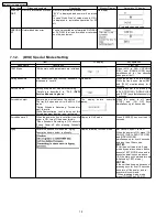
displayed, past 99 error histories
can be displayed by pressing [0] [1]
- [9] [9]

Delete

the

Last

Drive

Error

Delete the Last Drive Error information stored
on the DVD RAM-Drive.

Press [9] [6] in service mode.

23

DMR-EZ47VP / DMR-EZ475VP

Summary of Contents for DMR--EZ475VP

Page 1: ...sushita Electric Industrial Co Ltd All rights reserved Unauthorized copying and distribution is a violation of law Model No DMR EZ47VP DMR EZ475VP Vol 1 Colour K Black Type DVD Recorder ORDER NO CHM0704017CE B24 ...

Page 2: ...k Diagram 57 11 5 Analog Timer Block Diagram 58 11 6 System Control Servo Block Diagram 59 12 Schematic Diagram 61 12 1 Interconnection Schematic Diagram 61 12 2 Power Supply Section Power Digital I F P C B 1 3 Schematic Diagram P 63 12 3 Digital I F 1 4 Section Power Digital I F P C B 2 3 Schematic Diagram IF 65 12 4 Digital I F 2 4 Section Power Digital I F P C B 2 3 Schematic Diagram IF 66 12 5...

Page 3: ...14 2 Abbreviations 104 15 Parts and Exploded Views 110 15 1 Exploded Views 110 15 2 Replacement Parts List 114 3 DMR EZ47VP DMR EZ475VP ...

Page 4: ...potential across the resistor 4 Check each exposed metallic part and measure the voltage at each point 5 Reverse the AC plug in the AC outlet and repeat each of the above measurements 6 The potential at any point should not exceed 0 75 volts RMS A leakage current tester Simpson Model 229 or equivalent may be used to make the hot checks leakage current must not exceed 1 2 milliampere In case a meas...

Page 5: ...y 3 Use only a grounded tip soldering iron to solder or unsolder ES devices 4 Use only an anti static solder removal device Some solder removal devices not classified as anti static ESD protected can generate electrical charge sufficient to damage ES devices 5 Do not use freon propelled chemicals These can generate electrical charges sufficient to damage ES devices 6 Do not remove a replacement ES...

Page 6: ...2 2 Precaution of Laser Diode 6 DMR EZ47VP DMR EZ475VP ...

Page 7: ...Solder PbF The lead free solder has to be used when repairing the equipment for which the lead free solder is used Definition The letter of PbF is printed on the PCB using the lead free solder To put lead free solder it should be well molten and mixed with the original lead free solder Remove the remaining lead free solder on the PCB cleanly for soldering of the new IC Since the melting point of t...

Page 8: ...3 Service Navigation 3 1 Service Information 3 2 Caution for DivX 8 DMR EZ47VP DMR EZ475VP ...

Page 9: ...4 Specifications 9 DMR EZ47VP DMR EZ475VP ...

Page 10: ...5 Location of Controls and Components 5 1 Each Buttons 10 DMR EZ47VP DMR EZ475VP ...

Page 11: ...11 DMR EZ47VP DMR EZ475VP ...

Page 12: ...ned off 1 Turn off the power and press STOP CH UP keys on the front panel simultaneously for 5 seconds 6 1 1 2 DVD When the power can not be turned off 1 Press POWER key on the front panel for over 10 seconds to turn off the power forcibly and press STOP CH UP keys on the front panel simultaneously for 5 seconds 6 1 2 DVD When the Forcible Disc Eject can not be done 12 DMR EZ47VP DMR EZ475VP ...

Page 13: ...nd pull out AC cord 2 Remove the Top Case 3 Push in SLIDE CAM by Eject Pin JSJ0484 or minus screw driver small to eject tray slightly 4 Push out Tray by Eject Pin JZS0484 or minus screw driver small 13 DMR EZ47VP DMR EZ475VP ...

Page 14: ...ring to the Disassembly Procedures 2 Connect three batteries 1 5V spec to the Loading Motor in series for supplying 4 5V to rotate the Loading Motor as shown below 3 Stop unloading just before unloading will be completed as shown below and then the tape becomes slack as shown below 4 Rotate the S Reel by a small minus screwdriver to remove the slack tape as shown below 5 Then unload again to remov...

Page 15: ...tan Motor clockwise to remove the slack tape as shown below 5 Rotate the Main Cam Gear counter clockwise again to remove the cassette tape as shown below 6 Attach Loading Motor and tighten the screw 7 Set the Position Switch to EJECT POSITION certainly and attach the mechanism to chassis as shown below 15 DMR EZ47VP DMR EZ475VP ...

Page 16: ...U61 The unit is carrying out its recovery process No display U72 HDMI connection error communication error This error is displayed when there are any communication problems with the unit and the equipments TV amplifier etc connected to the unit by HDMI or when there is a problem with the HDMI cable U72 display disappears when error has been solved by Power OFF ON of connecting equipment or by inse...

Page 17: ... operate normally When device key information recorded is damaged No display F75 HDIM Device Key Information error HDMI connection could not be authenticated due to an internal data malfunction Factor of HDMI Device key road failure When HDMI LSI is damaged When the bus line of I2C doesn t operate normally When device key information recorded is damaged No display UNSUPPO RT Unsupported disc error...

Page 18: ... simultaneously for 5 seconds Forced disc eject Removing a disc that cannot be ejected The tray will open and unit will shift to P off mode During Schedule Recording Forced disc eject is invalid While Demonstration Lock is being set this Forced disc eject function is not accepted The display before execution leaves When the power is off press STOP and CH UP keys simultaneously for 5 seconds Forced...

Page 19: ...Item FL display Key operation Mode name Description Front Key Aging Contents Example 19 DMR EZ47VP DMR EZ475VP ...

Page 20: ...within 0 5 seconds When unlock the tray UNLOCK is displayed for 3 seconds When the power is on and tray being locked press STOP and POWER keys simultaneously for 5 seconds When press OPEN CLOSE key while the tray being locked Display LOCK for 3 seconds Press OPEN CLOSE key while the tray being locked Progressive initialization The progressive setting is initialized to Interlace The display before ...

Page 21: ...P switch 1 4 Initial mode is Interlace Press 1 1 in service mode Switch Interlace Progressive Press 1 4 in White Picture Output mode I P are switched alternately Magenta Picture Output Magenta picture is output with Component Output from AV Decoder Magenta picture Saturation rate 100 It is enable to switch Interlace Progressive by I P switch 1 4 Initial mode is Interlace Press 1 2 in service mode ...

Page 22: ...de Audio 48kHz Press 2 3 in service mode Audio 44 1kHz 48kHz switching Press 2 4 in Audio Pattern Output mode 48 kHz 44 1 kHz are switched alternately Laser Used Time Indiction Check laser used time hours of drive is the used time display in hour Laser used time of DVD CD in Playback Recording mode is counted Press 4 1 in service mode Delete the Laser Used Time Laser used time stored in the memory...

Page 23: ...conds 5 Last Drive Error code No 2 1 2 is displayed for 5 seconds This Error Code is unnecessory for service 6 Last Drive Error code No 2 2 2 is displayed for 5 seconds This Error Code is unnecessory for service 7 Error occurring Disc type is displayed for 5 seconds DISC 1 DVD DISC 2 CD DISC 3 DVD RAM 2 6GB DISC 4 DVD RAM 4 7GB DISC 5 DVD R DISC Unknown Disc 8 Unused No display 9 Factor of Drive E...

Page 24: ...oma signal and check the output on the S terminal Press 5 2 in service mode S2 signal output Forcibly superimpose the S2 signal approx 2V DC on the EE chroma signal and check the output on the S terminal Press 5 3 in service mode Front connection inspection Press all front keys and check the connection between Main P C B and Front key Switches 1 Each time a key is pressed segment turned on increas...

Page 25: ... 0 1 1 9 the past 19 error histories are displayed Delete the Error History Delete Error History information stored on the unit Press 9 7 in service mode Tray OPEN CLOSE Test The RAM drive tray is opened and closed repeatedly Press 9 1 in service mode When releasing this mode press the POWER button of Remote Controller more than 10 seconds Error code initialization Initialization of the last error...

Page 26: ...nder could not be started Error of the cylinder or the cylinder driver Yes Yes H02 The CAP FG could not be detected Yes Yes F03 Mechanism lock during without the unloading and the cassette up Yes Yes F04 Mechanism lock during unloading Yes Yes F05 S reel pulse cannot be detected when a cassette tape is inserted Error of the S reel system or the Capstan system No Yes F06 Mechanism lock during the C...

Page 27: ...ON SELECT to VHS When power is OFF press STOP and EJECT keys simultaneously for 3 seconds to into Service Mode In Service Mode press STOP and EJECT keys simultaneously to add Service Number 7 2 3 1 VHS Service Mode and Service Data at a glance Service Number Contents Contents of Indication on minute Contents of Indication on second Remarks 0 Indication for the inner data of IC6001 VHS mode Real ti...

Page 28: ...plementary data 1 and 2 of history 2 In these modes the supplementary data 3 and 4 instead of the Error number and supplementary data 1 and 2 are indicated only while pressing STOP key 5 Self diagnosis history 3rd Error number of history 3 Supplementary data 1 and 2 of history 3 6 Indication for the inner data of IC6001 Real time servo data 4 digits Real time Higher rank 1 BYTE of SERVO data Lower...

Page 29: ...mple of Display A Service Mode Number B Supplementary Data 3 Mechanism process shifting Number C Supplementary Data 4 LM Loading Motor information Display of means that Loading Motor turns ON when EJECT button was pressed but an error has occurred while mechanism was between REV position and LOAD position Supplementary Data 3 EJECT FF REW 10 PLAY passing REV 11 passing REV 12 passing REV LOAD Caps...

Page 30: ...ot be detected when a cassette tape is inserted Error of the S reel system or the Capstan system VHS mode Value of S Reel Pulse counted Process No 16 Detection of the Cylinder lock during the constant rotation VHS mode Tape position Process No 17 Detection of S reel lock during the constant tape running VHS mode Tape position Process No Number of FG 18 Detection of T reel lock during the constant ...

Page 31: ...exadecimal A 10 Decimal E 14 Decimal Hexadecimal indication from A to E are shown below Note 3 Supplementary Data 2 Reason of Ejection Supplementary Data 2 Reason 1 S reel pulse is less than 3 when the loading has been completed Miss catching the tape 2 Pulse Timer over during the short rewind at the DOWN position Error of S photo sensor system S reel system Capstan system 3 Mechanism lock from th...

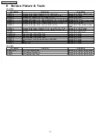
Page 32: ...55 ES30V ES40V Series RFKZ0239 Extension Cable Power Digital I F P C B Front R P C B 10 Pin Same as E75V ES30V Series RFKZ0260 Extension Cable Power Digital I F P C B Digital P C B 88 Pin Same as ES15 EH55 Series JZS0484 Eject Pin Same as ES15 E50 Series RFKZ03D01K Lead Free Solder 0 3mm 100g Reel Same as ES15 Series RFKZ06D01K Lead Free Solder 0 6mm 100g Reel Same as ES15 Series RFKZ10D01 Lead Fr...

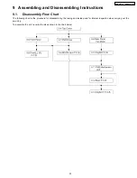
Page 33: ...isassembly Flow Chart The following chart is the procedure for disassembling the casing and inside parts for internal inspection when carrying out the servicing To assemble the unit reverse the steps shown in the chart below 33 DMR EZ47VP DMR EZ475VP ...

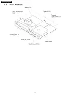
Page 34: ...9 2 P C B Positions 34 DMR EZ47VP DMR EZ475VP ...

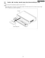
Page 35: ...e1 For description of the disassembling procedure see the section 9 4 Note2 Video Cassette might not enter when a strong lighting is applied to VHS Mechanism when Video Cassette is inserted Please weaken the lighting or cover with the top panel etc 35 DMR EZ47VP DMR EZ475VP ...

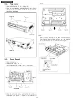
Page 36: ...1 Remove one screw A 2 Unlock 4 tabs in A D turn Pull with the front panel in the direction of your side 3 Make the unit turn inside out push the tabs E H by screwdriver while pulling Front panel in the direction of arrow Note When attaching Front Panel in order to hook Cassette Door Opener Lever to Cassette Door push up cassette door in the direction of arrow and insert a front panel 36 DMR EZ47V...

Page 37: ...and tab to remove Front R P C B 9 6 3 How to assemble Tray door ass y 1 Attach Blinder spling to Tray door ass y 2 Attach Tray door ass y in order from to Put the Brinder spring on the front panel Insert the shaft in the hole Insert the shaft in the hole 3 Confirm the Brinder spring is attached as following 37 DMR EZ47VP DMR EZ475VP ...

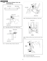
Page 38: ...inder Panel Step 2 Hook Blinder Spring to bottom of the shaft Step 3 Slide Blinder Panel into shaft hole of Front Panel Step 4 Slide down Blinder Panel to touch the shaft on top of the rib Step 5 Push shaft into shaft hole Step 6 Press centre of Blinder Panel and bow down 38 DMR EZ47VP DMR EZ475VP ...

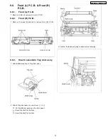
Page 39: ...9 7 DVD drive 1 Remove 3 Screws A 2 Disconnect FFC and Wire with connector remove DVD drive 9 8 SD DV Jack P C B 1 Remove 2 Screws A to remove SD DV jack P C B 39 DMR EZ47VP DMR EZ475VP ...

Page 40: ...9 2 Rear panel with fan motor 1 Disconnect Fan Connector 2 Remove 6 Screws B and 2 Screws C 3 Unlock 2 Locking Tabs A to remove Rear Panel with Fan Motor 9 10 Digital P C B 1 Remove 2 Screws A and 2 FFCs And lift up Digital P C B slightly so to disconnect connectors to remove Digital P C B 40 DMR EZ47VP DMR EZ475VP ...

Page 41: ...attention to stiff connections of P2571 and P3001 when removing VHS Mechanism Unit 9 11 1 Caution for attaching VHS Mechanism Unit 1 Because Position SW should be set to Eject Position refer to fig A and set the position switch so that the boss and arrow mark come on a straight line 2 Attach VHS Mechanism Unit so that Boss of Position SW is put into long hole of Main Cam Gear refer to Fig B 41 DMR...

Page 42: ...ectors 2 Remove 2 Screws A and remove Main P C B 9 13 Digital I F P C B 1 Remove 4 Screws A to remove DVD angle 2 Disconnect 4 Connectors 3 Remove the Screw B to remove Digital I F P C B after removed Rear angle 42 DMR EZ47VP DMR EZ475VP ...

Page 43: ...Measurements and Adjustments 10 1 Service Positions Note For description of the disassembling procedure see the section 9 10 1 1 Checking and Repairing of Power Digital I F P C B 43 DMR EZ47VP DMR EZ475VP ...

Page 44: ...10 1 2 Checking and Repairing of Main P C B 44 DMR EZ47VP DMR EZ475VP ...

Page 45: ...10 1 3 Checking and Repairing of Digital P C B 45 DMR EZ47VP DMR EZ475VP ...

Page 46: ...10 1 4 Checking and Repairing of DVD 46 DMR EZ47VP DMR EZ475VP ...

Page 47: ...placing Parts 10 2 1 Notice after replacing Digital P C B TM L1 is displayed after replacing Digital P C B Once power off and start up again 10 2 2 Items that should be done after replacing parts 47 DMR EZ47VP DMR EZ475VP ...

Page 48: ...48 DMR EZ47VP DMR EZ475VP ...

Page 49: ...49 DMR EZ47VP DMR EZ475VP ...

Page 50: ...10 3 Standard Inspection Specifications after Making Repairs After making repairs we recommend performing the following inspection to check normal operation 50 DMR EZ47VP DMR EZ475VP ...

Page 51: ...eck Item Contents Check Picture Block noise Sound Distorted sound Crosscut noise Noise static background noise etc Dot noise The sound level is too low Picture disruption The sound level is too high Not bright enough The sound level changes Too bright Flickering color Color fading 51 DMR EZ47VP DMR EZ475VP ...

Page 52: ...52 DMR EZ47VP DMR EZ475VP ...

Page 53: ...1 11 9 10 8 5 4 3 1 DMR EZ47VP EZ475VP Power Supply Block Diagram 1 2 4 3 FEED BACK Q1110 ON QR1350 Q1350 POWER ON OFF CONTROL H VCC 4 2 1 4 3 GND 3 HOT COLD IC1110 F B DRAIN 5 2 Z C RECTIFIER D1101 C1107 L1102 VA1101 L1101 F1101 ABSORBER SURGE AND SUPPRESSOR SURGE SWITCHING IC 1 P1101 AC SOCKET H H L DI P ON L H H H L CONT 1 V OUT 4 2 IC1200 REG DR 12V V IN DVD DRIVE TO QR7801 ON H Q7802 JC P ON ...

Page 54: ...OM IC6001 19 TO IC2501 H ON 3 V OUT REG A 5V A 5V DSC BIAS BIAS 5 1 IC2001 REG A 5V V IN 98 TO IC6001 H ON 1 V OUT A 9V 4 5 IC4803 REG A 9V V IN 30 TO IC4804 8 TO IC4805 1 21 TO IC2501 2 TO JK4801 JC 5V 19 P6003 P31903 4 TO IC3701 3 IC3902 25 40 44 52 64 72 78 8 TO IC4806 D1 POWER ON 23 FROM IC7501 6 3 TO T4001 Q4501 POWER SUPPLY QR4501 ON H H 12V 58 TO IC4501 5V 5V A D 5V A D 5V 25 40 TO IC4501 Q...

Page 55: ...CK JK4600 DVD VIDEO OUT 14 REAR A V OUT JACK JK3903 FRONT A V IN JACK JK3802 1 CLAMP TUNER 3 SECTION BLOCK DIGITAL FROM P3902 P31902 P31902 P3902 P3902 P31902 P3902 P31902 P3902 P31902 56 48 52 64 60 P37101 P56001 P56001 P37101 P37101 P56001 P37101 P56001 P37101 P56001 RPR OUT DM IIC CLOCK IC55001 IIC DATA IC55001 BPB OUT DM GPY OUT DM YOUT DM COUT DM 35 43 51 33 47 36 37 39 27 26 29 28 30 VIDEO P...

Page 56: ...GCL TO C CCD P EQ SQPB DL SQPB DET S PB DRIVER C CLOCK 2FSC OSCILLATOR VCO X TAL PB AGC APL REC FBC ALC ADJUSTMENT fo DEVIATION ET LPF MODULATION FM P FILTER REC DE EMPHASIS MAIN ACC DET CHROMA R ACC DET W C D C CARRIER OFFSET MAIN EMPHASIS ACC SW TRAP 629MHz REC APC LPF SUB KILLER SQPB PB APC DEMO APC SW AGC FM EQ SQPB DLIM DE EMPHASIS NON LINEAR VIDEO ALC G EQ CLAMP FEED BACK SYNC CLEAR ACC LPF ...

Page 57: ...L 9 R OUT 17 L OUT 18 10 9 8 P3001 P3001 7 P3001 Y3 Y2 Y1 Y0 X3 X2 X1 X0 Y X FM MIX TW4501 ENVE TW4502 IC3001 AUDIO PROCESSOR 3 P4002 4 P4002 AMP PRE EQ REC TRAP fh VCA P R 96 98 6 2 43 42 DVD R DVD L 64 15 10 14 63 9 22 24 29 27 21 30 57 53 62 61 BLOCK SECTION DIGITAL TO 24 20 L OUT R OUT REAR A V OUT JACK JK3902 DVD HEAD AUDIO Hi Fi R L CONTROL SYSTEM TO FROM 72 IC6001 IIC DATA IC6001 IIC CLOCK ...

Page 58: ...HS LED DRIVE QR27505 4 PP27501 5 6 4 P6001 P31905 P31906 PP27501 P6001 P31905 P31906 PP27501 P6001 P31905 P31906 PP27501 P6001 P31905 P31906 PP27501 P6001 P31905 P31906 PP27501 P6001 P31905 1 7 P31906 PP27501 P6001 P31905 7 2 3 TIMER DISPLAY VDD FAN LOCK 88 OUT FAN PWM 94 MAIN P C B FRONT R P C B TIMER CPU DP7501 28 7 29 1G 14 2G 11 3G 4 4G P16 6 P17 5 P18 P1 27 P2 26 P3 24 P4 23 P5 22 P6 20 P7 19...

Page 59: ...SW4 SW3 SW2 SW1 SW4 SW3 SW2 SW1 30 POSITION SW4 POSITION SW3 31 32 POSITION SW2 POSITION SW1 33 PB CTL OUT EX FF REW TW2002 97 82 6 5 P4002 1 P1531 2 P1531 P4002 HEAD CONTROL 95 94 COMPOSER FG PG AMPLIFIRE DIFFERENTIAL 17 16 15 CYL PFG 90 18 CYL ET CTL AMP REF 96 O REF 91 UNLOADING LOADING CAP FG IN CAP FG OUT 77 14 AMPLIFIRE DIFFERENTIAL COM M3 M2 M1 20 AMPLIFIRE DIFFERENTIAL SELECTOR GENERATOR S...

Page 60: ...DMR EZ47VP DMR EZ475VP 60 ...

Page 61: ...1 2 3 4 5 6 7 8 9 10 1 2 3 4 5 6 18 17 16 15 14 13 12 11 19 9 10 8 P31903 7 VHS LED P6001 RST KEY DUB LED DVD LED KEY3 KEY2 KEY1 VHS LED KEY1 KEY2 KEY3 DVD LED DUB LED RST KEY 7 3 4 2 5 1 6 6 5 4 3 2 1 7 P31905 1 2 3 4 5 6 18 17 16 15 14 13 12 11 19 9 10 8 P31904 7 P3902 IECOUT D5V I2C5CK I2C5DT CPN CIN DM GND V YIN DM YOUT DM GND GND BPBOUT DM GPYOUT DM RPROUT DM XDMUTE COUT DM GND GND GND GND IE...

Page 62: ...13 12 12 11 11 10 10 9 9 8 8 7 7 6 6 5 5 4 4 3 3 2 2 1 1 A B C 22 21 20 19 18 17 16 15 14 13 12 P11101 N A SLIGHTLY DIFFERNT OR AMENDED SINCE THIS DRAWING WAS PREPARED THE CORRECT PART NUMBER IS SHOWN IN THE PARTS LIST AND MAY BE NOTE DO NOT USE THE PART NUMBER SHOWN ON THIS DRAWING FOR ORDERING DMR EZ47VP EZ475VP Interconnection Schematic Diagram DMR EZ47VP EZ475VP Interconnection Schematic Diagr...

Page 63: ...0003 6 3V 1200P C1430 G0A100HA0023 L1420 10V 1800 C1420 D1430 B0JAQE000004 D1420 B0JAQE000004 D1432 B0JCPD000021 10V 680 C1421 6 3V 560P C1431 16V 560 C1440 C1131 2700P B0AACK000004 D1132 C1133 330P MAZ73000BC D1131 1K D R1135 20K D R1134 1000P C1132 C1134 3900P 10K R1132 2400 D R1374 22K R1372 C1371 0 047 100 D R1376 G0A100HA0023 L1001 820 D R1375 2400 D R1378 3300 R1373 0 1 C1372 A R 3 2 C 1 IC1...

Page 64: ... VCC STARTUP ON VCC STARTUP OFF CIRCUIT START UP PROTECTION 4 ON OFF DRIVE 5 3 1 2 REG AMP VREF VIN VOUT ON H GND ADJ GND VIN VOUT VC 3 2 4 1 IC IC1001 D 2 3V SWITCHING REGULATOR IC DETAIL BLOCK DIAGRAM IC1200 DR 12V SWITCHING REGULATOR IC DETAIL BLOCK DIAGRAM IC1430 D 3 3V SWITCHING REGULATOR IC DETAIL BLOCK DIAGRAM IC1400 F SWITCHING REGULATOR IC DETAIL BLOCK DIAGRAM IC1110 1130 SWITCHING IC IC ...

Page 65: ... MOTOR K1KA03AA0180 K1KA03AA0301 FANLOCK TU TU TU TU TU or GND G_RFC_A_IN_A G_RFC_V_IN_A GND or FANDCOUT VIN ON H VOUT A IN GND A OUT A IN B IN B IN V B OUT NR MGND GND AFC GND MGND CH_SW P JC_PON D3R3V X_SW6V X_SW6V FANPWM1 UNREG_38V JC_REG5V X_SW12R3V MECHA_12R3V DR_PON_H FANLOCK1 MECHA_12R3V D5V GND GND GND GND GND GND GND GND I2C5CK AUGND AUGND TUN_R TUN_L AUGND ADC_L ADC_R AUGND XDMUTE COUT_D...

Page 66: ..._LED DVD_LED GND KEY2 KEY3 DVD_LED DUB_LED VHS_LED KEY1 P P P F F GND GND SCLK VPP XFWE XINTP XINTM SBMTP SBPTM XMPREQ TV_VCR RST_KEY UARTP2M UARTM2P DI_PON_H HDMI_MONI D HDMI_CONT HDMI_P5_ON_H 18 19 20 17 16 15 14 13 12 11 TO DIGITAL I F SECTION 4 4 LOCATION MAP 1 4 2 4 3 4 4 4 DMR EZ47VP EZ475VP Digital I F 2 4 Section Power Digital I F P C B 2 3 Schematic Diagram IF NOTE DO NOT USE THE PART NUM...

Page 67: ...02 4 5 6 7 2 1 3 IC31001 C0DBGHF00001 T1R5V G_I2C5CK_A G_TU_SDA_A G_TUIFOUT1_A G_TU_IFAGC_A G_TUIFOUT2_A G_TU_SCL_A G_I2C5DT_A TV_VCR D2R3V AFC JC_REG5V JC_P_ON_H CH_SW D3R3V X_SW_5R8V GND DI_PON_H D_P_OFF_L1 X_SW_3R2V X_SW_12R5V X_SW_4V MM1775AFBE S 815A50AMC CN GND P P P P P P P P P P NC TU TU TU TU TU TU TU TU TU TU TU TU SUB ON H VIN VOUT CNT GND VIN GND CN NC VOUT NC VIN NC ON H MM1683DFBE NO...

Page 68: ...LB37103 ERJ3GEY0R00V CL37115 XINTM SBMTP DGND HDMI_CONT DGND XINTP UART2_RX SCLK UART2_TX HDMI_MONI SBPTM DGND DGND DGND DGND DGND DGND DGND AU5V DGND DGND DGND DGND DGND DGND XFWE DGND I2CCK I2CDT AUGND AUGND AUGND AUGND AUGND IECOUT XDMUTE AADC_R AADC_L COUT_DM YOUT_DM GPYOUT_DM BPBOUT_DM RPROUT_DM MIXROUT_DM MIXLOUT_DM V_YIN_DM CPNCIN_DM XMPREQ HDMI_PLUG D5V P_OFF_DL_L DGND DGND DGND DGND DGND ...

Page 69: ...6 3V 47P C7823 G_SIF_B JC_REG5V 0 047 C7308 C7322 50V 2 2 100 R7301 R7302 100 C7301 6 3V 22P ERJ3GEY0R00V K7801 1K R7307 C7807 1u 3 1 2 4 5 C0CBCDC00052 IC7801 10V 1 C7802 G_SIF_C 3 1 2 EFCT4R5MS5W J0B4504AA026 FL7301 R7308 0 C7319 1u G_SIF_E C7316 1u C7313 16V 10P 0 1 C7312 GND C7306 50V 4 7 C7302 50V 4 7 C7305 50V 4 7 C7304 6 3V 22P C7314 50V 2 2 1u C7317 C7310 6 3V 47P 0 01 C7311 R7306 4700 C73...

Page 70: ...65 64 67 66 69 68 71 70 73 72 75 74 80 77 78 76 79 81 84 58 59 56 57 54 55 52 53 39 40 37 38 35 36 33 34 31 32 50 49 47 48 45 46 43 44 41 42 51 29 2 3 1 5 7 9 8 6 4 27 23 24 19 20 15 16 11 12 10 14 13 18 17 22 21 26 25 28 30 C1AB00002083 IC3001 S S S A A A S A A S S A A A A L SP L SP R A R 2SC1959 Y S S I I I S I S S S S A S S S VIDEO ENVE FM_MUT S S or A S HA118425BNF E MESECAM Det MIX LEVEL SW37...

Page 71: ...SB0710A0L TL1002 820 D R4504 K4513 VWJ0795 5 L4501 1R2u K4702 VWJ0795 20 R4513 4700 QR4501 UNR521100L R4507 4700 R4506 1K C4527 16V 10P C4528 16V 10P 6800 R4527 OUT_NORMAL R4526 24K C4521 16V 10P C4529 16V 10P DVD_OUT_R R4505 6800 R4501 56K R4502 6800 C4524 0 1 KB C4526 16V 10P S FM MIX V V I V ENVE S S S V V I I I TV EXT4 S V S I I V V I V I V I EXT4 S V S I I I I I TV L SW22 MIX MUTE SW19 R SW21...

Page 72: ...EY2 79 77 76 78 49 47 48 50 74 71 72 67 68 56 55 58 57 52 51 54 53 65 66 61 62 59 60 64 63 70 69 73 75 10 8 7 9 12 11 99 100 95 94 96 97 90 91 89 93 92 98 4 6 5 2 1 3 81 82 80 86 87 88 84 83 85 45 19 17 15 14 16 18 43 23 21 20 22 41 24 39 37 33 35 34 29 30 27 26 28 32 31 36 38 25 40 42 44 13 46 MN67789CA IC7501 MAZ4091NHF D7507 0 1 C6100 GND GND VPP PSAVEH P17 P16 F NX 4G P18 P14 P12 3G P13 4G P15...

Page 73: ...072 VHS_CS IR A_H_SW GND SENSOR HSW JC_PON AFC GND S PHOTO or or UARTM2P UARTP2M SCLK HDMI_MONI DI_PON_H HDMI_P5_ON_H GND TV_VCR TEST2 HDMI_CONT T PHOTO D3R3V DR_PON_H S REEL X_SW12R3V JC_REG5V T REEL UNREG_38V MECHA_12R3V MECHA_12R3V VOUT VSS VIN V H NC ON I I I I A V X_SW6V X_SW6V FANLOCK1 MGND MGND V A V I I V A FANPWM1 TO DVD I F CH_SW F F VPP XFWE XINTM XINTP XMPREQ GND SBPTM SBMTP TO DVD I F...

Page 74: ... 41 44 42 43 48 50 30 39 37 35 32 31 34 33 36 38 40 22 23 26 28 27 24 25 53 55 57 59 58 56 54 29 52 1000P C6014 29 CH_SW 28 FM_MUTE 30 POS SW4 BIAS H PB X5 H TAB SW SAFETY S_TAB L AVR L ABS_NORM 52 CVOUT CVIN2 EP H HLF VHOLD 53 OSD5V NUA GND L3 CPS H 51 KILLER IR POS SW1 A A I I I I 5V D GND L2SW GND L2_LIN L2_VIN2 CPN_C_IN2 CPN_Y_IN2 KEY1 GND L2_RIN POS SW3 or or PFAIL MODE SW AD5V POS SW2 12MHz ...

Page 75: ...4 CL6006 CL6005 CL6003 R6012 220 R6029 220 R6023 220 3 4 2 5 98 94 95 92 91 93 97 96 1 100 99 80 78 76 77 79 87 86 88 89 82 84 83 81 85 90 16 14 15 17 11 13 12 69 67 65 64 66 68 70 20 21 18 19 62 60 61 63 75 73 71 72 74 9 7 6 8 10 C2CBHF000474 IC6001 TIMER_CS ART V H N REMOCON VIDEO H SW TEST2 D REC H AUDIO H SW VM2 M3 S_CASE RNF OUT1 1 L1L2SWIDEB CTL HEAD CTL AMP REF 3 L3_S1S2 4 L3_DET 2 CODE CTL...

Page 76: ...PG AMPLIFIRE DIFFERENTIAL 17 16 15 18 14 AMPLIFIRE DIFFERENTIAL COM M3 M2 M1 20 AMPLIFIRE DIFFERENTIAL SELECTOR GENERATOR SIGNAL DRIVE MOTOR PRE DRIVE DRIVE MOTOR 25 23 22 4 2 OUT 2 OUT 1 AMP AMP PRE DRIVE LOGIC CONTROL R IN EC PFG F IN 6 5 Vref VCC VOUT 2 1 3 OUT VDD GND 1 3 2 Vref IC7501 TIMER IC DETAIL BLOCK DIAGRAM IC7503 RESET IC DETAIL BLOCK DIAGRAM IC2001 6301 5V SWITCHING REG IC DETAIL BLO...

Page 77: ...01 2 1 4 7 9 3 10 5 8 15 18 16 13 21 19 22 23 24 17 20 12 14 JK3902 K1U717B00005 C3711 0 1 KB R3707 1M G0C220JA0019 L3702 AV2 G IN TEST1 DVD Y IN DRV GND1 VREF DVCC1 DRV VCC2 DET OUT B 21 Y 3 IN 22 DRV GND2 41 DVD C IN C S DET2 Y 2 IN DGND1 BH7622KS2 C 1 IN VIDEO 2 IN DVD G PY IN DVD B PB IN V75 SAG V75 OUT PB C75 OUT C S DET3 PR DVD_V_OUT Y COM_CPN_OUT Y C DVD_CPN_OUT C Y75 OUT VIDEO 3 IN Y75 SAG...

Page 78: ...8 K1U718B00003 JK3903 DVD_OUT_H A_GND R3937 470 C3926 1u KB 1u KB C3925 R4808 100K R4855 100K R4856 100K 100K R4809 C4809 16V 10P QR4807 UNR511300L C4810 16V10P C4807 16V 220P R4812 1K R4813 1K 6 7 5 2 4 3 8 1 C0ABBB000228 IC4802 C4808 0 01 1K R4824 1K R4825 1 2 4 3 14 15 16 13 IC4801 C0JBAR000438 MM1507XNRE COM LOUT COM VOUT COM ROUT A CPN L1 IN Y A C LINE IN1 L CPS L1 IN LINE IN1 R S S A S S S C...

Page 79: ...20P C4845 R4848 47K C4847 16V 100P R4845 10K F 16V 47P C4850 R4841 560 10K R4839 1000P C4830 SYNC_DET 6 7 5 2 4 3 8 1 IC4806 C0ABBB000216 XTMUTE X_SW12R3V X_SW_5R8V D4801 MA2C165001VT TUN_L TUN_R TO P31901 POWER DIGITAL I F P C B DIGITAL I F SECTION 8 9 13 11 10 12 2 3 1 5 7 6 4 15 14 P3901 K1KB15AA0032 6 7 5 2 4 3 8 1 IC4805 C0ABBB000119 C4814 16V 100P IN2 VO1 VCC IN1 VO2 IN1 A VIN GND NR VOUT ON...

Page 80: ...13 14 11 12 3 1 2 30 32 31 4 29 IC4804 C1AB00001920 C4803 16V 10P C4805 16V 10P R4814 47K 7 5 6 10 12 11 8 9 UNR521300L QR4810 S S A S A A POFF_H SELECT RF_OUT or LS EXT32 RF BIAS BD3824FS E2 D A2 LINE OUT2 VCC OUTR LINEOUT1 OUTL FRONT1 FRONT2 D A1 SDA GND SCL REGFIL NC TUOL CAP1 TUOR NC VHS AUDIO OUT TUIR TUIL NC X0 A B X3 Y1 VSS VEE lnhlblt EXT11 EXT22 EXT31 EXT12 EXT21 1 2 3 4 5 6 7 8 9 10 11 1...

Page 81: ...N C2 IN VIDEO3 IN VIDEO2 IN TUNER 7 10 5 21 24 14 17 19 12 1 CLAMP TUNER 3 35 43 51 33 47 36 37 39 27 26 29 28 30 41 20 C S DET3 6 C S DET1 48 DET OUT B V Y SW B MIX B C SW B Y SW B MIX B V SW B 0dB 0dB Y V OUT A COUT A 65 69 0 6dB VIDEO A SLICER 67 VDD VEE VSS SW LOGIC Y2 X2 X1 X0 Y3 Y1 X3 A INH B Y0 X Y 16 15 14 13 12 11 10 9 1 2 3 4 5 6 7 8 32 10 9 29 28 31 18 21 20 INTERFACE IIC BUS SDA SCL TU...

Page 82: ...1 3 4 2 20 19 P66802 TO P56501 DIGITAL P C B AVENC RTSC AVDEC MAIN CPU 2 K1MY20AA0021 2 1 4 3 P66803 DV JACK K1FY104B0006 TPB TPB CLK GND WP GND CMD COM DAT1 DAT3 FG SD CARD DAT2 3R3V DAT0 TPA CD FG TPA GND D3R3V DAT2 D3R3V TPA WP GND CMD DAT3 GND TPB TPA GND TPB GND CD DAT1 DAT0 GND CLK 8 9 10 7 6 E F G D C 5 4 3 2 1 B A DMR EZ47VP EZ475VP DV Jack SD Card Schematic Diagram NOTE DO NOT USE THE PAR...

Page 83: ...V GND KEY 1 L2 IN R EJECT POWER 5 4 3 2 1 A B C DMR EZ47VP EZ475VP Front L Schematic Diagram 12 20 Front R Schematic Diagram S27506 S27507 R27516 2700 B3ACA0000273 D27503 QR27505 D27501 B3AAA0000752 QR27501 QR27503 R27505 390 R27501 270 R27503 390 S27509 D27505 B3ADA0000173 2200 R27532 R27502 1500 R27508 1500 S27502 S27504 S27501 R27517 2200 S27508 1500 R27509 S27510 6 8 9 7 2 1 4 5 3 10 PP27501 K...

Page 84: ...DMR EZ47VP DMR EZ475VP 84 ...

Page 85: ...rd 13 1 Power Digital I F P C B 13 1 1 Power Digital I F P C B 1 4 Section 1 A B C D 2 3 4 5 DMR EZ47VP EZ475VP Power Digital I F P C B VEP09147A 1 4 Section REAR FRONT 1 4 2 4 3 4 4 4 Location Map DMR EZ47VP DMR EZ475VP 85 ...

Page 86: ...13 1 2 Power Digital I F P C B 2 4 Section 5 6 7 8 9 DMR EZ47VP EZ475VP Power Digital I F P C B VEP09147A 2 4 Section REAR FRONT 1 4 2 4 3 4 4 4 Location Map DMR EZ47VP DMR EZ475VP 86 ...

Page 87: ...3 1 3 Power Digital I F P C B 3 4 Section C D E Power Digital I F P C B DMR EZ47VP EZ475VP Power Digital I F P C B VEP09147A 3 4 Section REAR FRONT 1 4 2 4 3 4 4 4 Location Map DMR EZ47VP DMR EZ475VP 87 ...

Page 88: ...13 1 4 Power Digital I F P C B 4 4 Section HOT COLD DMR EZ47VP EZ475VP Power Digital I F P C B VEP09147A 4 4 Section REAR FRONT 1 4 2 4 3 4 4 4 Location Map DMR EZ47VP DMR EZ475VP 88 ...

Page 89: ... 3 D1300 C 6 LB7810 C 8 C1402 E 2 C37108 B 7 R7302 B 8 QR31002 B 3 D1301 C 6 LB7811 C 8 C1403 E 2 C37111 B 6 R7304 B 8 D1350 C 5 LB7812 C 8 C1410 E 6 C37112 B 6 R7305 B 8 CL1201 E 3 D1351 C 5 LB7813 C 7 C1420 E 6 C37114 B 6 R7306 B 8 CL1202 E 3 D1400 E 6 LB7814 C 7 C1421 E 5 C45002 B 7 R7307 B 7 CL1203 E 3 D1410 E 6 LB7815 C 7 C1430 D 5 C45003 B 7 R7308 B 8 CL37101 B 6 D1412 E 2 LB7816 C 8 C1431 D...

Page 90: ...13 2 Main P C B 13 2 1 Main P C B 1 4 Section 1 A B C D 2 3 4 5 DMR EZ47VP EZ475VP Main P C B VEP06G37A 1 4 Section REAR FRONT Location Map 1 4 2 4 3 4 4 4 DMR EZ47VP DMR EZ475VP 90 ...

Page 91: ...13 2 2 Main P C B 2 4 Section 5 6 7 8 9 DMR EZ47VP EZ475VP Main P C B VEP06G37A 2 4 Section REAR FRONT Location Map 1 4 2 4 3 4 4 4 DMR EZ47VP DMR EZ475VP 91 ...

Page 92: ...13 2 3 Main P C B 3 4 Section Main P C B C D E F DMR EZ47VP EZ475VP Main P C B VEP06G37A 3 4 Section REAR FRONT Location Map 1 4 2 4 3 4 4 4 DMR EZ47VP DMR EZ475VP 92 ...

Page 93: ...13 2 4 Main P C B 4 4 Section DMR EZ47VP EZ475VP Main P C B VEP06G37A 4 4 Section REAR FRONT Location Map 1 4 2 4 3 4 4 4 DMR EZ47VP DMR EZ475VP 93 ...

Page 94: ...002 C 5 TL7504 D 2 LB3104 B 7 C3017 D 4 C3926 C 6 C4803 C 7 C6012 C 2 R3031 D 4 R4514 C 5 R4842 E 7 R7523 E 2 Q4081 A 2 TL7507 E 2 LB3105 C 7 C3019 D 4 C3927 C 6 C4804 C 6 C6014 B 3 R3032 C 5 R4515 B 5 R4843 E 7 R7525 D 2 Q4084 A 2 LB3106 B 7 C3020 D 4 C3928 C 6 C4805 C 7 C6015 B 3 R3035 C 4 R4516 C 5 R4844 E 7 R7527 F 1 Q4501 A 6 J1 D 5 LB3107 A 7 C3021 D 4 C3932 B 7 C4806 C 6 C6016 B 3 R3046 B 4...

Page 95: ...B 1 A B C D 2 3 4 5 6 7 8 9 DV Jack SD Card P C B Foil Side DMR EZ47VP EZ475VP DV Jack SD Card P C B Foil Side VEP73144A Component Side DMR EZ47VP EZ475VP DV Jack SD Card P C B Component Side VEP73144A DMR EZ47VP DMR EZ475VP 95 ...

Page 96: ...13 4 Front L P C B Front R P C B 1 A B C D E 2 3 4 5 6 7 8 9 DMR EZ47VP EZ475VP Front L P C B VEP04915A Front R P C B VEP07B00A Front L P C B Front R P C B DMR EZ47VP DMR EZ475VP 96 ...

Page 97: ... 4 0 2 2 5 0 5 0 2 4 2 8 2 4 2 3 2 4 2 4 2 5 2 5 5 0 2 0 Ref No MODE 21 22 23 24 REC 2 4 1 5 2 4 2 4 PLAY 2 4 1 5 2 4 2 4 STOP 2 4 1 5 2 4 2 4 Ref No MODE 1 2 3 4 5 1 2 3 4 5 6 7 REC 5 9 0 5 9 5 0 5 0 0 3 4 4 8 0 5 9 PLAY 5 9 0 5 9 5 0 5 0 0 3 4 4 8 0 5 9 STOP 5 9 0 5 9 5 0 5 0 0 3 4 4 8 0 5 9 Ref No MODE 1 2 3 4 5 6 7 8 1 2 3 4 5 REC 3 3 1 3 0 4 6 4 0 5 9 0 4 1 5 0 PLAY 3 3 1 3 0 4 6 4 0 5 9 0 4 ...

Page 98: ...E 1 2 3 4 5 6 7 8 9 10 11 12 13 14 15 16 17 18 19 20 REC 1 8 0 1 7 5 0 1 8 4 8 1 4 4 7 0 1 2 8 0 1 4 4 8 1 4 0 0 1 2 7 0 1 4 4 8 PLAY 1 8 0 1 7 5 0 1 8 4 8 1 4 4 7 0 1 2 8 0 1 4 4 8 1 4 0 0 1 2 7 0 1 4 4 8 STOP 1 8 0 1 7 5 0 1 8 4 8 1 4 4 7 0 1 2 8 0 1 4 4 8 1 4 0 0 1 2 7 0 1 4 4 8 Ref No MODE 21 22 23 24 25 26 27 28 29 30 31 32 33 34 35 36 37 38 39 40 REC 1 4 0 0 1 2 7 4 9 1 7 1 7 1 9 1 9 2 2 0 2...

Page 99: ...0 0 4 0 2 2 4 2 4 2 4 1 0 1 0 4 6 2 5 2 4 4 8 4 8 4 5 PLAY 0 0 0 0 0 0 0 4 0 2 2 4 2 4 2 4 1 0 1 0 4 6 2 5 2 4 4 8 4 8 0 2 STOP 0 0 0 0 0 0 0 4 0 2 2 4 2 4 2 4 1 0 1 0 4 6 0 2 4 4 8 5 0 0 2 Ref No MODE 81 82 83 84 85 86 87 88 89 90 91 92 93 94 95 96 97 98 99 100 REC 0 0 0 0 0 2 5 2 5 0 0 1 3 2 5 2 5 0 2 3 2 8 2 5 2 5 5 1 4 9 0 PLAY 0 0 0 0 0 2 5 2 5 0 0 1 3 2 5 2 5 0 2 3 2 8 2 5 2 5 5 1 4 9 0 STOP...

Page 100: ...0 0 1 10 1 10 1 9 4 PLAY 0 0 0 1 0 0 0 1 10 1 10 1 9 4 STOP 0 0 0 1 0 0 0 1 10 1 10 1 9 4 Ref No MODE E C B E C B E C B E C B E C B REC 5 1 28 1 4 8 0 0 1 4 8 0 0 4 6 0 0 0 0 0 0 PLAY 5 1 5 0 0 0 5 7 0 0 0 4 6 0 0 0 0 0 0 STOP 5 1 5 0 0 0 5 7 0 0 0 4 6 0 0 0 0 0 0 Ref No MODE E C B E C B E C B E C B E C B REC 0 0 0 5 9 0 1 5 9 0 0 0 1 0 0 2 2 0 5 9 0 PLAY 0 0 0 5 9 0 1 5 9 0 0 0 1 0 0 2 2 0 5 9 0 ...

Page 101: ...8 4 9 0 0 3 3 0 0 0 5 1 2 1 0 0 STOP 3 3 1 4 0 0 4 9 4 9 0 0 5 8 4 9 0 0 3 3 0 0 0 5 1 2 1 0 0 Ref No MODE 41 42 43 44 45 46 47 48 49 50 51 52 53 54 55 56 57 58 59 60 REC 3 3 1 2 3 3 0 0 0 3 5 0 6 3 5 0 3 5 0 5 0 0 12 2 0 6 0 0 1 7 0 7 PLAY 3 3 1 2 3 3 0 0 0 3 5 0 6 3 5 0 3 5 0 5 0 0 12 2 0 6 0 0 1 7 0 7 STOP 3 3 1 2 3 3 0 0 0 3 5 0 6 3 5 0 3 5 0 5 0 0 12 2 0 6 0 0 1 7 0 7 Ref No MODE 61 62 63 64 ...

Page 102: ...LAY 0 2Vp p 20usec div IC3001 80 REC PLAY 0 5Vp p 10msec div IC4501 21 TW4501 REC 1 1Vp p 20usec div IC3001 86 REC 1 4Vp p 20usec div IC6001 80 FF REW 5 0Vp p 1msec div IC6001 95 REC 2 4Vp p 10msec div IC3001 6 REC PLAY 0 9Vp p 2msec div IC3001 19 REC 1 0Vp p 20usec div IC3001 29 REC PLAY 2 4Vp p 20usec div IC3001 36 PLAY 0 5Vp p 20usec div IC4501 57 REC PLAY 1 6Vp p 0 5msec div IC4501 53 REC PLAY...

Page 103: ...4 STOP 36Vp p 5usec div P37101 60 REC PLAY 0 8Vp p 20usec div P37101 52 REC PLAY 1 0Vp p 20usec div P37101 48 REC PLAY 0 6Vp p 20usec div P37101 64 REC PLAY 1 0Vp p 20usec div P37101 78 80 REC PLAY 0 8Vp p 1msec div JK3902 3 REC PLAY 2 0Vp p 20usec div JK3902 4 REC PLAY 1 5Vp p 20usec div JK3902 16 REC PLAY 2 0Vp p 20usec div P37101 42 REC PLAY 1 0Vp p 20usec div T1130 4 STOP 20Vp p 2msec div T111...

Page 104: ...P OUT SIGNAL DATA REQUEST DATA RESPONSE DIGITAL SERVO CONTROLLER DATA SLICE LOOP FILTER DIGITAL VIDEO DISC INITIAL LOGO ABBREVIATIONS E EC ECR ENCSEL ETMCLK ETSCLK ERROR TORQUE CONTROL ERROR TORQUE CONTROL REFERENCE ENCODER SELECT EXTERNAL M CLOCK 81MHz 40 5MHz EXTERNAL S CLOCK 54MHz F FBAL FCLK FE FFI FEO FG FSC FSCK FOCUS BALANCE FRAME CLOCK FOCUS ERROR FOCUS ERROR AMP INVERTED INPUT FOCUS ERROR...

Page 105: ... SUB CODE CLOCK SUB CODE Q DATA SYSTEM CLOCK T TE TIBAL TID TIN TIP TIS TPSN TPSO TPSP TRCRS TRON TRSON TRACKING ERROR BALANCE CONTROL BALANCE OUTPUT 1 BALANCE INPUT BALANCE INPUT BALANCE OUTPUT 2 OP AMP INPUT OP AMP OUTPUT OP AMP INVERTED INPUT TRACK CROSS SIGNAL TRACKING ON TRAVERSE SERVO ON INITIAL LOGO ABBREVIATIONS V VBLANK VCC VCDCONT VDD VFB VREF VSS V BLANKING COLLECTOR POWER SUPPLY VOLTAG...

Page 106: ...DIO OUTPUT L AUDIO OUTPUT R AUDIO SELECT H AUDIO L AUDIO R AV CONTROL AV CONTROL AV CONTROL SERIAL CLOCK AV CONTROL MODE AV CONTROL LEVEL METER R AV SW LEVEL METER L B MODE H BURST GATE PULSE BACK UP 5V BAND U BAND VL BILINGUAL MIX L BIL BIL L BIL H BIL M1 L BS CLOCK BS DATA BS LCH IN BS MIX H BS MON H BS MONI H BS RCH IN BS VIDEO BS VIDEO BS1 BS H BS LEVEL BS M H BS VTR H BUS CLK BUS LSN BUS TLK ...

Page 107: ...E H FM OUTPUT L FM OUTPUT R FM PACK OUTPUT L FM PACK OUTPUT R FM BS SELECT L FM BS SELECT R FS CLOCK FULL ERASE HEAD ON H FULL ERASE HEAD ON H FULL E 12V GND A GND TU GND N SW 12V H SYNC H AMP SW H P R H P L H P GND H P OUT L H P OUT R H SW HEAD PHONE L HEAD PHONE R HEAD SW HEATER HEATER HSS HTR HTR I RFE ICL IF IN SELA1 IN SELA2 IN SELA3 INS L R L INS H INSEL A1 INSEL A2 INSERT INSERT H IO CS JOG...

Page 108: ...AL H NR BIAS NTSC L CONTROL AGC CIRCUIT OUTPUT P OFF H P OFF L P FAIL P OFF H P OFF L PAL H PAL L NTSC H PB ADJ OUT PB OUT PB H PFG PHOTSN B PICT CNT PLAY LED RVS LED PLAY PO PLAY R LED PLY DEW POWER OFF L PREROLL H PWRFAIL R CH H R CH L R ST R S F RCH H REC 12V REC CHROMA REC H REC IN REC OUT L REC START REC VR C REC VR L REC VR R REC Y REC H REC C REC Y REC EE CTL REEL T REEL S REGULATOR FILTER ...

Page 109: ... STOP 2 POSITION STOP 2 POSITION SAFETY TAB SW STEREO H SUB BIAS SUB SW S VHS CASSETTE L SW 5V DETECT SYNC L SYSCON 5V SYSTEM T PHOTO T RL PLS T BUSCLK T BUSLSN T BUSTLK T END L T PHOTO TAPE END L TAPE END L CAM TEST TPZ TRIC L TRICK L TRK ENV TU AUDIO TU GND TU V IN TU VIDEO TUN NOR IN TUN R TUN AUDIO IN TUNER 12V TUNER L TUNER V IN TUNER L TUNER N TUNER R TUNER 12 TUOFF H TV AUDIO TV VTR TXTON L...

Page 110: ...15 Parts and Exploded Views 15 1 Exploded Views 15 1 1 Casing Parts Mechanism Section1 110 DMR EZ47VP DMR EZ475VP ...

Page 111: ...15 1 2 Casing Parts Mechanism Section 2 111 DMR EZ47VP DMR EZ475VP ...

Page 112: ...15 1 3 VHS Mechanism Section 112 DMR EZ47VP DMR EZ475VP ...

Page 113: ...15 1 4 Packing Accessories Section 113 DMR EZ47VP DMR EZ475VP ...

Page 114: ... C3010 ECJ1VB0J105K 6 3V 1U 1 Ref No Part No Part Name Description Pcs Remarks C3011 F1H1C104A071 16V 0 1U 1 C3012 F2A0J470A824 6 3V 47P 1 C3013 F2A1C100B099 16V 10P 1 C3014 F1H1C104A071 16V 0 1U 1 C3015 ECJ1VB0J105K 6 3V 1U 1 C3016 F1H1C104A071 16V 0 1U 1 C3017 F1H1C104A071 16V 0 1U 1 C3019 F1H1C104A071 16V 0 1U 1 C3020 F2A1H3R3B032 50V 3 3U 1 C3021 F2A1V100A824 35V 10U 1 C3023 ECJ1VB1H103K 50V 0...

Page 115: ... C4819 F2A1C221B111 16V 220P 1 C4820 F2A1H1R0B040 50V 1U 1 C4821 ECJ1VC1H820J 50V 82P 1 C4822 ECJ1VF1C104Z 16V 0 1U 1 Ref No Part No Part Name Description Pcs Remarks C4823 ECJ1VB1H103K 50V 0 01U 1 C4827 ECJ1VF1C104Z 16V 0 1U 1 C4828 ECJ1VC1H820J 50V 82P 1 C4829 F2A1C101B110 16V 100P 1 C4830 ECJ1VB1H102K 50V 1000P 1 C4831 F1H1C104A071 16V 0 1U 1 C4832 F2A0J470A599 6 3V 47U 1 C4833 ECQV1H104JL3 50V...

Page 116: ...55 CONNECTOR 8P 1 P3001 K1MN09A00022 CONNECTOR 9P 1 P3901 K1KB15AA0032 CONNECTOR 15P 1 P3902 K1KB19AA0032 CONNECTOR 19P 1 P4001 K1KB02A00035 CONNECTOR 2P 1 P4002 K1MN06A00033 CONNECTOR 6P 1 P6001 K1KB07AA0032 CONNECTOR 7P 1 P6002 K1KB19AA0032 CONNECTOR 19P 1 P6003 K1KB19AA0032 CONNECTOR 19P 1 PS6001 K1KB12B00047 CONNECTOR 12P 1 Q1501 PNB2303M01VT TRANSISTOR 1 Q1502 PNB2303M01VT TRANSISTOR 1 Q3001 ...

Page 117: ...ERJ3GEYJ563V 1 10W 56K 1 R4516 ERJ3GEYJ622V 1 10W 6 2K 1 R4517 ERJ3GEYJ473V 1 10W 47K 1 Ref No Part No Part Name Description Pcs Remarks R4518 ERJ3GEYJ622V 1 10W 6 2K 1 R4519 ERJ3GEYJ753V 1 10W 75K 1 R4520 ERJ3GEYJ472V 1 10W 4 7K 1 R4521 ERJ3GEYJ511V 1 10W 510 1 R4522 ERJ3GEYJ511V 1 10W 510 1 R4523 ERJ3GEYJ103V 1 10W 10K 1 R4524 ERJ3GEYJ753V 1 10W 75K 1 R4525 ERJ3GEYJ102V 1 10W 1K 1 R4526 ERJ3GEYJ...

Page 118: ...ITCH MODE 1 T4081 G2A472C00003 TRANSFORMER 1 W701 ERJ3GEY0R00V 1 10W 0 1 W702 ERJ8GEY0R00V 1 4W 0 1 W703 ERJ3GEY0R00V 1 10W 0 1 W704 ERJ3GEY0R00V 1 10W 0 1 Ref No Part No Part Name Description Pcs Remarks W705 ERJ8GEY0R00V 1 4W 0 1 W706 ERJ8GEY0R00V 1 4W 0 1 W707 ERJ8GEY0R00V 1 4W 0 1 W708 ERJ8GEY0R00V 1 4W 0 1 W709 ERJ8GEY0R00V 1 4W 0 1 W710 ERJ8GEY0R00V 1 4W 0 1 W711 ERJ8GEY0R00V 1 4W 0 1 W712 E...

Page 119: ...ame Description Pcs Remarks S27509 EVQ11G07K SWITCH SELECT 1 S27510 EVQ11G07K SWITCH RESET 1 VEP73144A SD DV JACK P C B 1 RTL C66802 F1H1A225A051 10V 22U 1 LB66801 J0JHC0000032 COIL 1 LB66802 J0JHC0000045 COIL 1 P66801 K1NA09E00083 CONNECTOR 9P 1 P66802 K1MY20AA0021 CONNECTOR 20P 1 P66803 K1FY104B0006 CONNECTOR 4P 1 R66812 ERJ3GEYJ820V 1 10W 82 1 R66814 ERJ3GEYJ820V 1 10W 82 1 R66815 ERJ3GEYJ330V ...

Page 120: ...000003 DIODE 1 D1130 B0AADM000003 DIODE 1 D1131 MAZ73000BC DIODE 1 D1132 B0AACK000004 DIODE 1 D1133 B0BC010A0007 DIODE 1 D1200 B0JCNG000003 DIODE 1 D1201 B0JCNG000003 DIODE 1 D1300 B0JAME000025 DIODE 1 D1301 B0JAME000025 DIODE 1 Ref No Part No Part Name Description Pcs Remarks D1350 MA2J11100L DIODE 1 D1351 MA2J11100L DIODE 1 D1400 B0JAME000025 DIODE 1 D1410 B0AADM000003 DIODE 1 D1420 B0JAQE000004...

Page 121: ... ERJ3RED470V 1 16W 47 1 R1358 ERJ3RBD242V 1 16W 2 4K 1 R1361 ERJ3GEYJ332V 1 10W 3 3K 1 R1362 ERJ3GEYJ103V 1 10W 10K 1 R1363 ERJ3GEYJ472V 1 10W 4 7K 1 Ref No Part No Part Name Description Pcs Remarks R1370 ERJ3GEYJ391V 1 10W 390 1 R1371 ERJ3GEYJ102V 1 10W 1K 1 R1372 ERJ3GEYJ223V 1 10W 22K 1 R1373 ERJ3GEYJ332V 1 10W 3 3K 1 R1374 ERJ3RBD242V 1 16W 2 4K 1 R1375 ERJ3RBD821V 1 16W 820 1 R1376 ERJ3RBD101...

Page 122: ...B1431 TENSION ARM BOSH 1 105 VDG1686 INTERMEDIATE GEAR 1 106 VDG1685 MAIN CAM GEAR 1 107 VDG1512 IDLER GEAR 2 108 VDG1514 CHANGE GEAR 1 109 VDR0372A REEL TABLE 2 110 VDV0391 CAPSTAN BELT 1 Ref No Part No Part Name Description Pcs Remarks 111 VEM0797 LOADING MOTOR 1 112 VMB3550A CHANGING GEAR SPRING 1 113 VMD4987 WORM SHAFT HOLDER 1 114 VMD5466 OPENER PIECE 1 115 VMD4253 LED PRISM 1 116 VML3934 MAI...

Reviews: