1
2
34
56
78
9
X
Y
1
A
B
C
D
E
F
G
H
A
B
C
D
E
F
G
23
4
5
6
7
8
9
X
Y
41876101TH Rev. 1
40 /
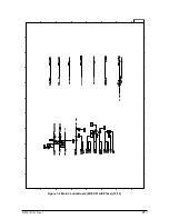
Figure 1-7 Memory Expansion Bord (MM7-PCB) (2/4)
Note 1 For the group 1G of Q1, the contact pin locations can be interchanged freely
within the group 1G of Q1 so long as the input-to-output relationship is maintained.
Note 2 For Q2, the pin locations can be interchanged freely within Q2 so long as the
input-to-output relationship is maintained.

