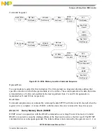


Background Debug Mode (BDM) Interface
MCF5253 Reference Manual, Rev. 1
Freescale Semiconductor
20-31
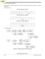
ADDRESS[31:0]–High Address
This field contains the 32-bit address which marks the upper bound of the address breakpoint range.
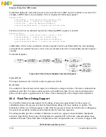
20.5.2
Address Attribute Trigger Register
The AATR defines the address attributes and a mask to be matched in the trigger. The AATR value is
compared with the address attribute signals from the processor’s local high-speed bus, as defined by the
setting of the TDR. The AATR is accessible in supervisor mode as debug control register $6 using the
WDEBUG instruction and through the BDM port using the WDMREG command. The lower five bits of
the AATR are also used for BDM command definition to define the address space for memory references
as described in
Section 20.4.1.2, “Debug Module Hardware.”
Access: User write only
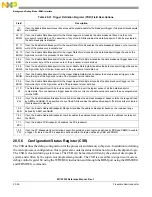
31
30
29
28
27
26
25
24
23
22
21
20
19
18
17
16
R
W
ADDRESS[31:0]
Reset
–
–
–
–
–
–
–
–
–
–
–
–
–
–
–
–
15
14
13
12
11
10
9
8
7
6
5
4
3
2
1
0
R
W
ADDRESS[31:0]
Reset
–
–
–
–
–
–
–
–
–
–
–
–
–
–
–
–
Figure 20-30. Address Breakpoint High Register (ABHR)
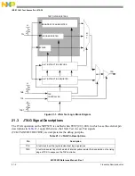
Access: User write only
15
14
13
12
11
10
9
8
7
6
5
4
3
2
1
0
R
W
RM
SZM
TTM
TMM
R
SZ
TT
TM
Reset
0
0
0
0
0
0
0
0
0
0
0
0
0
1
0
1
Figure 20-31. Address Attribute Trigger Register (AATR)
Table 20-19. Address Attribute Trigger Register Field Descriptions
Field
Description
15
RM
The Read/Write Mask field corresponds to the R-field. Setting this bit causes R to be ignored in address
comparisons.
14–13
SZM
The Size Mask field corresponds to the SZ field. Setting a bit in this field causes the corresponding bit in SZ
to be ignored in address comparisons.
12–11
TTM
The Transfer Type Mask field corresponds to the TT field. Setting a bit in this field causes the corresponding
bit in TT to be ignored in address comparisons.
10–8
TMM
The Transfer Modifier Mask field corresponds to the TM field. Setting a bit in this field causes the
corresponding bit in TM to be ignored in address comparisons.
7
R
The Read/Write field is compared with the R/W signal of the processor’s local bus.
Summary of Contents for MCF5253
Page 1: ...Document Number MCF5253RM Rev 1 08 2008 MCF5253 Reference Manual...
Page 26: ...MCF5253 Reference Manual Rev 1 xxvi Freescale Semiconductor...
Page 32: ...MCF5253 Reference Manual Rev 1 xxxii Freescale Semiconductor...
Page 46: ...MCF5253 Introduction MCF5253 Reference Manual Rev 1 1 14 Freescale Semiconductor...
Page 62: ...Signal Description MCF5253 Reference Manual Rev 1 2 16 Freescale Semiconductor...
Page 98: ...Instruction Cache MCF5253 Reference Manual Rev 1 5 10 Freescale Semiconductor...
Page 104: ...Static RAM SRAM MCF5253 Reference Manual Rev 1 6 6 Freescale Semiconductor...
Page 128: ...Synchronous DRAM Controller Module MCF5253 Reference Manual Rev 1 7 24 Freescale Semiconductor...
Page 144: ...Bus Operation MCF5253 Reference Manual Rev 1 8 16 Freescale Semiconductor...
Page 176: ...System Integration Module SIM MCF5253 Reference Manual Rev 1 9 32 Freescale Semiconductor...
Page 198: ...Analog to Digital Converter ADC MCF5253 Reference Manual Rev 1 12 6 Freescale Semiconductor...
Page 246: ...DMA Controller MCF5253 Reference Manual Rev 1 14 18 Freescale Semiconductor...
Page 282: ...UART Modules MCF5253 Reference Manual Rev 1 15 36 Freescale Semiconductor...
Page 344: ...Audio Interface Module AIM MCF5253 Reference Manual Rev 1 17 46 Freescale Semiconductor...
Page 362: ...I2 C Modules MCF5253 Reference Manual Rev 1 18 18 Freescale Semiconductor...
Page 370: ...Boot ROM MCF5253 Reference Manual Rev 1 19 8 Freescale Semiconductor...