


DMA Controller
MCF5253 Reference Manual, Rev. 1
Freescale Semiconductor
14-3
14.3
DMA Module Overview
The DMA controller module usually transfers data at rates much faster than the ColdFire core under
software control can handle. The term DMA refers to the ability for a peripheral device to access memory
in a system in the same manner as the core. DMA operations can greatly increase overall system
performance.
The DMA module consists of four independent channels. The term DMA is used throughout this section
to reference any of the four channels, as they are all functionally equivalent. It is impossible to implicitly
address all four DMA channels at the same time.
DMA requests can be generated by the processor writing to the START bit in the DMA control register or
generated by an on-chip peripheral device asserting one of the REQUEST signals. The processor can
program the amount of bus bandwidth allocated for the DMA for each channel. The DMA channels
support continuous and cycle-steal transfer modes.
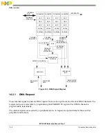
The DMA controller supports dual-address transfers. In dual-address mode, the DMA channel supports 32
bits of address and 32 bits of data. Dual-address transfers can be initiated by either a processor request
using the START bit or by an internal peripheral device using the REQUEST signal. Two bus transfers
occur in this mode, a read from a source device and a write to a destination device (see
).
Any operation involving the DMA module follows the same three basic steps:
1. Channel initialization step—The DMA channel registers are loaded with control information,
address pointers, and a byte transfer count. Also, the DMAROUTE register is programmed to
control the source of the internal requests.
2. Data transfer step—The DMA accepts requests for operand transfers and provides addressing and
bus control for the transfers.
3. Channel termination step—This occurs after operation is complete. The channel indicates the
status of the operation in the channel status register.
Figure 14-2. Dual Address Transfer
DMA
MEMORY
or
MEMORY
-
MAPPED
PERIPHERAL
MEMORY
or
MEMORY
-
MAPPED
PERIPHERAL
Summary of Contents for MCF5253
Page 1: ...Document Number MCF5253RM Rev 1 08 2008 MCF5253 Reference Manual...
Page 26: ...MCF5253 Reference Manual Rev 1 xxvi Freescale Semiconductor...
Page 32: ...MCF5253 Reference Manual Rev 1 xxxii Freescale Semiconductor...
Page 46: ...MCF5253 Introduction MCF5253 Reference Manual Rev 1 1 14 Freescale Semiconductor...
Page 62: ...Signal Description MCF5253 Reference Manual Rev 1 2 16 Freescale Semiconductor...
Page 98: ...Instruction Cache MCF5253 Reference Manual Rev 1 5 10 Freescale Semiconductor...
Page 104: ...Static RAM SRAM MCF5253 Reference Manual Rev 1 6 6 Freescale Semiconductor...
Page 128: ...Synchronous DRAM Controller Module MCF5253 Reference Manual Rev 1 7 24 Freescale Semiconductor...
Page 144: ...Bus Operation MCF5253 Reference Manual Rev 1 8 16 Freescale Semiconductor...
Page 176: ...System Integration Module SIM MCF5253 Reference Manual Rev 1 9 32 Freescale Semiconductor...
Page 198: ...Analog to Digital Converter ADC MCF5253 Reference Manual Rev 1 12 6 Freescale Semiconductor...
Page 246: ...DMA Controller MCF5253 Reference Manual Rev 1 14 18 Freescale Semiconductor...
Page 282: ...UART Modules MCF5253 Reference Manual Rev 1 15 36 Freescale Semiconductor...
Page 344: ...Audio Interface Module AIM MCF5253 Reference Manual Rev 1 17 46 Freescale Semiconductor...
Page 362: ...I2 C Modules MCF5253 Reference Manual Rev 1 18 18 Freescale Semiconductor...
Page 370: ...Boot ROM MCF5253 Reference Manual Rev 1 19 8 Freescale Semiconductor...