NXP Semiconductors LS1028ARDB Getting Started Manual Download Page 8

8 DIP switches

The LS1028ARDB provides dual inline package (DIP) switches to allow easy configuration of the system for the most popular
board options. The CPLD stores the DIP switch values in the BRDCFG and DUTCFG registers and that allows the software (either
local or remote) to reconfigure the system as required.

For each DIP switch:

• If the switch is up (on), the value is 1

• If the switch is down (off), the value is 0

Figure 4. 

on page 5 shows the switches available on the board.

The table below shows the available switches, and also indicates the default switch settings as shipped.

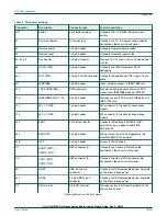
Table 6. Switch settings

Switch

Supported function

Description

SW2[1:4]

RCW fetch location

CFG_RCW_SRC[3:0]

SW_RCW_SRC[3:0]

• 0000: Hard-coded RCW

• 1000: SDHC1: SD card

• 1001: SDHC2: eMMC

• 1010: UEFI/I2C Boot EEPROM

• 1101: XSPI serial NAND, 4K pages

• 1111: XSPI serial NOR, 24-bit address (default setting)

SW2[5]

Reset mode

RESET_REQ_B

SW_RST_MODE

• 0: Ignore RESET_REQ_B

• 1: Trigger system reset on RESET_REQ_B (default setting)

SW2[6:8]

XSPI_A device mapping

CFG_XSPI_MAP

SW_XSPIMAP[2:0]: Controls how XSPI_A chip-selects are connected to
devices/peripherals.
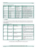
Table 7.

Bit value

XSPI_A_CS0

XSPI_A_CS1

Description

000 (default
setting)

sNOR

sNAND

Normal NOR

001

sNAND

sNOR

Normal NAND

010

Emulator

sNOR

Programmable
NOR

011

Emulator

sNAND

Programmable
NAND

100

sNOR

Emulator

Boot from sNOR
and program
emulator

NXP Semiconductors

DIP switches

QorIQ LS1028A Reference Design Board Getting Started Guide, Rev. 0, 2/2019

User's Guide

8 / 18

Summary of Contents for LS1028ARDB

Page 1: ...on Link how to access QorIQ LS1028A Reference Design Board Reference Manual Provides detailed description of the LS1028ARDB QorIQ LS1028A Reference Design Board Reference Manual QorIQ LS1028A Product...

Page 2: ...Development Studio for QorIQ LS series ARM V8 ISA Targeting Manual CodeWarrior TAP Probe User Guide Provides details of CodeWarrior TAP which enables target system debugging through a standard debug p...

Page 3: ...ow shows the back panel of the LS1028ARDB chassis J1 Power Jack J10 Display Port J22 USB2 J21 USB1 P2 SD card slot J14 SGMII Ethernet port J15 QSGMII Ethernet ports Figure 2 LS1028ARDB chassis back pa...

Page 4: ...J34 J2 J9 J16 J18 J20 J5 Figure 3 LS1028ARDB connectors The following image shows the push buttons jumpers LEDs and switches on the LS1028ARDB board NXP Semiconductors Chassis and board pictures QorIQ...

Page 5: ...functions of these push buttons Table 3 LS1028ARDB push buttons Push button Label Function Description SW1 PWR Power cycle Press PWR to turn the power ON or OFF SW4 RST System reset Press RST to rese...

Page 6: ...d IEEE 1722 pins J17 M 2_1 COEX 1x4 pin header M 2 connector 1 header for coexistence signals J19 M 2_2 COEX 1x4 pin header M 2 connector 2 header for coexistence signals J23 EMU 2x10 pin connector Co...

Page 7: ...sed to select some options which either do not change often or involve power conduction Figure 4 on page 5 shows the jumpers available on the board The table below describes the factory default settin...

Page 8: ...SW2 1 4 RCW fetch location CFG_RCW_SRC 3 0 SW_RCW_SRC 3 0 0000 Hard coded RCW 1000 SDHC1 SD card 1001 SDHC2 eMMC 1010 UEFI I2C Boot EEPROM 1101 XSPI serial NAND 4K pages 1111 XSPI serial NOR 24 bit a...

Page 9: ...ration CFG_MUX_UART2_SEL0 SW_UART2MAP 1 0 0x UART2 on DB9 connector default setting 10 UART2 on mikroBUS click module 1 11 UART2 on mikroBUS click module 2 SW3 7 PWM configuration CFG_MUX_PWM2uBUS1_B...

Page 10: ...s routed to TX only SAI transceiver default setting The table below summarizes the switch settings of the LS1028ARDB DIP switches for eMMC boot SDHC2 and SD boot SDHC1 Table 9 Switch settings for eMMC...

Page 11: ...hich generally indicates Improper RCW source selection Boot memory does not contain a valid RCW PBL PLL multipliers in the RCW data are not compatible with the fixed SYSCLK DDRCLK or SDCLK values D26...

Page 12: ...e LS1028ARDB board chassis Figure 1 on page 3 shows the LEDs available on the board chassis Table 11 LEDs available on front panel of board chassis Reference designator LED color LED name Description...

Page 13: ...ble 13 Reset sequencer state on page 13 Not applicable M 3 0 reflect contents of the LED register M2 Not applicable M1 Not applicable M0 Heartbeat Clock monitor Table 13 Reset sequencer state State LE...

Page 14: ...machine Host computer to control and monitor the LS1028ARDB board from the serial console using a serial terminal emulator such as Tera Term for Windows platform or Minicom for Linux platform NOTE In...

Page 15: ...the other end of the cable to the USB port of the host machine This connection allows you to make a console connection between the board and host computer to see the console output 9 Optionally connec...

Page 16: ...00 00000000 00000000 00000000 00000050 00000000 00000000 00000000 00000000 00000060 00000000 00000000 200e705a 00000000 00000070 bb580000 00000000 Model NXP Layerscape 1028a RDB Board Board LS1028AE R...

Page 17: ...lowing steps in case console does not show any print Ensure that the board is configured for the default switch settings For detail see DIP switches on page 8 Ensure that the power cord is connected t...

Page 18: ...not convey any license under its patent rights nor the rights of others NXP sells products pursuant to standard terms and conditions of sale which can be found at the following address nxp com SalesTe...

Reviews: