


UM11158
All information provided in this document is subject to legal disclaimers.
© NXP B.V. 2022. All rights reserved.
User manual
Rev. 1.6 — 17 March 2022
16 of 24
NXP Semiconductors
UM11158
LPCXpresso55S69/55S28 Development Boards
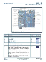
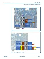
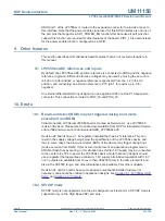
7. On-board
peripherals
This section describes how the on-board peripheral devices of the Board are connected to
the LPC55Sxx and relevant configuration options. For full details of these devices please
refer to the individual device datasheets. For circuit further details, refer to the board
schematics.
7.1 Audio Codec
The LPCXpresso55S69 board incorporates a Cirrus Logic (Wolfson) WM8904 audio
codec. This codec has both I2C (for control) and I2S (for data) interfaces.
The I2C interface of the codec is routed to Flexcomm 4 of the LPC55Sxx, the same
connection as used for the other I2C devices on the board; the Codec has an address of
0b0011010.
The Flexcomm 6 and Flexcomm 7 interfaces of the LPC55Sxx are connected respectively
to the Codec for data sent to / receive from the Codec. The board design assumes pad
sharing between Flexcom 6 and Flexcom 7 for I2S connections.
I2S connections from the LPC55Sxx are also connected to the Expansion connectors;
solder jumpers may be removed to disconnect the on-board codec if an external I2S
device is to be used instead.
Line input (J1) and line output (J2) 1/4” stereo jack sockets provide analog I/O
connections to the Codec. See schematic for further information.
7.2 Micro SD card slot
The micro SD card (P21) included in the LPCXpresso55S69 board provides a 4-bit SDIO
interface to support memory cards, plug-in WiFi modules, etc. Power enable to the socket
is provided via transistor enabled by P1_0.
Software drivers and related examples for the SD card are provided as part of the
MCUXpresso SDK.
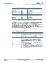
Table 2.
Audio Codec port connections
Circuit reference
Port
Flexcoms
I2S SCK
P0_21
Flexcom 6 & 7, pad shared
I2S TX/RX Data
P0_20
Flexcom 6 & 7, pad shared
I2S WS
P0_19
Flexcom 6 & 7, pad shared
I2C SDA
P1_21
Flexcom 4
I2C SCL
P1_20
Flexcom 4
Table 3.
Micro SD card connections
SDIO interface signals
Port
Notes
SDIO Clock
P0_7
IOCON function 2
SDIO Command
P0_8
IOCON function 2
D0
P0_9
IOCON function 2
D1
P0_17
IOCON function 2
D2
P0_24
IOCON function 2