NXP Semiconductors LPC55S69-EVK User Manual Download Page 9

UM11158

All information provided in this document is subject to legal disclaimers.

© NXP B.V. 2018. All rights reserved.

User manual

Rev. 0.2 — 16 October 2018 

9 of 20


NXP Semiconductors

UM11158

LPCXpresso55S69 Development Board

3. Getting 

started

NOTE: Pre-production boards released are not set up with final out-of-box demo 
code, and debug probes listed may not yet support this product. The J-link version 
for Link2 to support this product is not yet available

This section describes how to first power up the board and then how to start a first debug 
session using the MCUXpresso SDK. The board is pre-programmed with a simple 
program indicating that the target MCU is running. Connect a micro USB cable from 
connector P5 to a host computer or power supply to power-up the board and run this 
program. 

The following debug probes can be used with those development and the board (check 
compatibility between debug probe and IDE used, including support for Arm Cortex M33 
cores): 

On-board debug probe (LPC4322 “Link2”)

LPC-Link2 (OM13054) debug probe from NXP or Embedded Artists
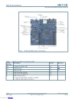
P21

SD card slot
8-bit, full size card slot connected to the LPC55S69 SD0 interface. 
Supports 3.3V operation only.

n/a

P23, P24

Mikroe Click site
Provides connectivity to standard Mikroe Click connectors. Shares SPI, 

ADC, I2C and USART connections with the P16-P19 expansion 

connectors.

n/a

P25

A header may be added at P25 to provide a convenient way to 

enable/disable the on-board accelerometer. If this header is used, 
remove the zero ohm resistor R20, which is in parallel with this header.

Not installed

P28

ADC0 differential input connector. This header provides access to the 
ADC0 negative and positive inputs, plus a ground pin.

n/a

S1

ISP/User button
When pressed, this button connect sport pin P0_5 to ground. Hold this 
button down while pressing and releasing Reset (S4) to force the 
LPC55S69 into ISP mode. Port P0_5 may also be reconfigured as a 
GPIO in user application code to enable this button to be used for other, 
user-defined purposes. A 2.2k ohm pull up is used to pull P0_5 high 
when the button is not pressed.

n/a

S2

Wake/User button
This button, when pressed, pulls P1_18 to ground. A 100K ohm pull up 
to VDD is connected to P1_18.

S3

User button
This button, when pressed, pulls P1_9 to ground. A 100K ohm pull up 
to VDD is connected to P1_9, and this port is also connected to pin 1 of 
expansion connector P18.

S4

Reset button
When pressed, reset is applied to the LPC55S69, expansion connector 
(Arduino reset) P16, the Mikroe Click site reset, and U14 (debug 
connector P7 reset when debugging an off-board target).

Table 1.

Indicators, buttons, connectors and LEDs

Circuit 
reference

Description

Default

Reference

Downloaded from

Arrow.com.

Downloaded from

Arrow.com.

Downloaded from

Arrow.com.

Downloaded from

Arrow.com.

Downloaded from

Arrow.com.

Downloaded from

Arrow.com.

Downloaded from

Arrow.com.

Downloaded from

Arrow.com.

Downloaded from

Arrow.com.

Summary of Contents for LPC55S69-EVK

Page 1: ...158 LPCXpresso55S69 Development Board Rev 0 2 16 October 2018 User manual Document information Info Content Keywords LPC55S69 LPC55xx LPCXpresso55S69 LPC55S69 EVK Abstract LPCXpresso55S69 user manual...

Page 2: ...more information please visit http www nxp com For sales office addresses please send an email to salesaddresses nxp com NXP Semiconductors UM11158 LPCXpresso55S69 Development Board Revision history...

Page 3: ...tp www nxp com demoboard LPCXpresso55S69 for more information on this board including tutorial videos development software and board hardware design files Note the schematics for this board indicate c...

Page 4: ...ard RGB user LED Reset ISP User Wakeup and user buttons Multiple Expansion options including Arduino UNO Mikroe Click and PMod Micro SD card slot NXP MMA8652FCR1 accelerometer Stereo audio codec with...

Page 5: ...Board layout and Settings Figure 2 shows the layout of the board top side indicating location of the connectors and buttons while Figure 3 shows locations of jumpers and headers Table 1 provides a des...

Page 6: ...s and LEDs Circuit reference Description Default Reference DS1 Target power indicator LED n a n a DS2 Link2 boot LED n a 4 1 D8 RGB User LED n a n a J1 Audio codec line input jack n a J2 Audio codec l...

Page 7: ...1 2 for USB1 High Speed to provide Vbus i e enable USB host capability Default Install jumper in position 2 3 for USB0 Full Speed to provide Vbus i e enable USB host capability 1 2 USB1 J7 USB host p...

Page 8: ...re current consumption Not installed P13 Current measurement header for LPC55S69 This header is in line with the VDD supply of the LPC55S69 with a zero ohm resistor R92 installed in parallel with it T...

Page 9: ...A header may be added at P25 to provide a convenient way to enable disable the on board accelerometer If this header is used remove the zero ohm resistor R20 which is in parallel with this header Not...

Page 10: ...steps for use with MCUXpresso IDE Download and install the MCUXpresso IDE Configure and download an SDK package with the MCUXpresso IDE tool chain option selected from the MCUXpresso SDK Builder utili...

Page 11: ...ll be five devices if using CMSIS DAP protocol four under Human Interface Devices CMSIS DAP LPC SIO two HID Compliant Devices and a USB Input Device and one under Ports LPC LinkII Ucom Your board is n...

Page 12: ...se the Link2 device on the LPCXpresso55S69 required for any debugging purpose for Windows 7 or 8 host computers install the drivers first These drivers will automatically be installed when MCUXpresso...

Page 13: ...going to the Windows operating system Start menu and typing Device Manager in the search bar In the device manager look under Ports the LPC LinkII UCom Port device and its name should be visible NOTE...

Page 14: ...4 Note that the MMA8652 Accelerometer and use of most SD cards requires the board to be configured for 3 3V operation The power connection to the Accelerometer may be disconnected by removing R20 inst...

Page 15: ...PMod connector and that jumper P1 is installed to disable the connection to the Link2 7 On board peripherals This section describes how the on board peripheral devices of the Board are connected to t...

Page 16: ...the supply rail and P25 may be installed to provide a convenient way to connect disconnect it to from power Resistors R3 and R4 are zero ohm links provided to enable the MMA8652 to be disconnected fro...

Page 17: ...t ISP when the LPC55S69 is reset or powered up This jumper is in parallel with S1 7 5 2 User S3 and Wake S2 buttons The User S3 and Wake S2 buttons are intended for user application use These buttons...

Page 18: ...oaded from Arrow com Downloaded from Arrow com Downloaded from Arrow com Downloaded from Arrow com Downloaded from Arrow com Downloaded from Arrow com Downloaded from Arrow com Downloaded from Arrow c...

Page 19: ...r severe property or environmental damage NXP Semiconductors accepts no liability for inclusion and or use of NXP Semiconductors products in such equipment or applications and therefore such inclusion...

Page 20: ...urrent 14 6 Board serial connections 14 6 1 LPC55S69 USB Ports 14 6 2 USART header 15 7 On board peripherals 15 7 1 Audio Codec 15 7 2 Micro SD card slot 15 7 3 Accelerometer 16 7 4 RGB User LED 16 7...

Reviews: