


Distributor of NXP Semiconductors: Excellent Integrated System Limited
Datasheet of MCIMX53SMD - TABLET SABRE PLATFORM MCIMX53
Contact us: [email protected] Website: www.integrated-circuit.com
66
MCIMX53SMD Board Hardware User’s Guide, Rev. 0
Freescale Semiconductor
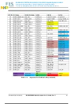
J78 PIN J13 Name
ALT(4)
ALT(5)
ALT(6)
ALT(7)
26
CSI0_DAT12
USBH3_DATA0
DEBUG_PC6
EMI_DEBUG41 tpiu TRACE9
28
CSI0_DAT13
USBH3_DATA1
DEBUG_PC7
EMI_DEBUG42 tpiu TRACE10
29
I2C2_SDA
i2c2 SDA
32K_OUT
ccm PLL4_BYP usb1 LINESTATE0
31
I2C2_SCL
i2c2 SCL
ecspi1 SS3
fec CRS
usb1 SIECLOCK
32
CSI0_DAT14
USBH3_DATA2
DEBUG_PC8
EMI_DEBUG43 tpiu TRACE11
33
DISP0_RESET
34
CSI0_DAT15
USBH3_DATA3
DEBUG_PC9
EMI_DEBUG44 tpiu TRACE12
35
CSI0_PIXCLK
DEBUG_PC0
EMI_DEBUG29
38
PCLOCK
uart2 TXD_MUX
firi RXD
spdifPLOCK
ccm PLL2_BYP
40
SPDIF_TX
CE_RTC_FSV_TRIG spdif OUT1
SNOOP2
JTAG_ACT
43
DISP0_DCLK
DEBUG_CORE_STATE0
EMI_DEBUG0
usb1 AVALID
44
CSI0_DAT16
USBH3_DATA4
DEBUG_PC10
EMI_DEBUG45 tpiu TRACE13
46
CSI0_DAT17
USBH3_DATA5
DEBUG_PC11
EMI_DEBUG46 tpiu TRACE14
50
CSI0_DAT18
USBH3_DATA6
DEBUG_PC12
EMI_DEBUG47 tpiu TRACE15
52
CSI0_DAT19
USBH3_DATA7
DEBUG_PC13
EMI_DEBUG48 usb2 BISTOK
53
SCSI0_PWDN
usb1 VSTATUS3
56
CSI0_VSYNCH
DEBUG_PC3
EMI_DEBUG32 tpiu TRACE0
58
CSI0_HSYNCH
DEBUG_PC1
59
CSI0_RSTB
usb1 VSTATUS2
62
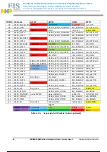
DISP0_DAT0
DEBUG_CORE_RUN
EMI_DEBUG5
usb2 TXREADY
63
GPIO_0(CLK0) EPITO
SRTC_ALARM_DEB
USBH1_PWR
csu TD
64
DISP0_DAT1
DEBUG_EVENT_CHAN_SEL
EMI_DEBUG6
usb2 RXVALID
66
DISP0_DAT2
DEBUG_MODE
EMI_DEBUG7
usb2 RXACTIVE
68
DISP0_DAT3
DEBUG_EVENT_BUS_ERROR EMI_DEBUG8
usb2 RXERROR
70
DISP0_DAT4
DEBUG_BUS_RWB
EMI_DEBUG9
usb2 SIECLOCK
72
DISP0_DAT5
DEBUG_MATCHED_DMBUS
EMI_DEBUG10 usb2 LINESTATE0
74
DISP0_DAT6
DEBUG_RTBUFFER_WRITE
EMI_DEBUG11 usb2 LINESTATE1
76
DISP0_DAT7
DEBUG_EVENT_CHANNEL0
EMI_DEBUG12 usb2 VBUSVALID
78
DISP0_DAT8
DEBUG_EVENT_CHANNEL1
EMI_DEBUG13 usb2 AVALID
Legend
UART4
AUDMUX4
I2C1
ECSPI2
USBH2
UART5
AUDMUX5
I2C2
CSPI
SPDIF
Table 6-15. Expansion Port Pin-Mux Table (continued)
67 / 82
67 / 82