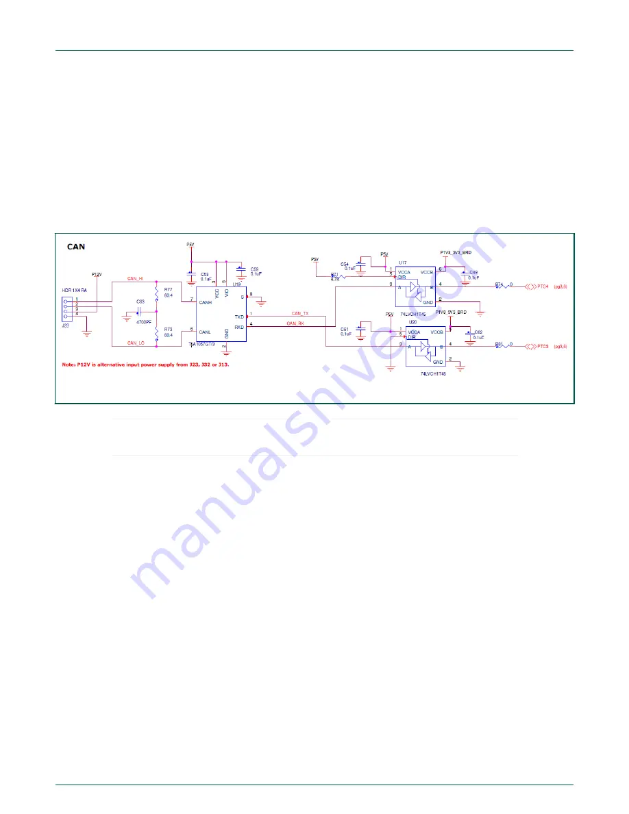
NXP Semiconductors FRDMKW36UG User Manual Download Page 21

3.10 CAN interface

U19 is the NXP TJA1057 high speed CAN transceiver. It provides an interface between a Controller Area Network (CAN) protocol
and the physical two-wire CAN bus. The transceiver is designated for high speed CAN applications in the automotive industry,
providing the differential transmit and receive capability to a CAN protocol controller. 

Figure 25

 shows the CAN Interface circuit.

• The TJA1057 power supply is P5V coming from the U15 (regulator) device.
• J23 provides pins to interface with a CAN bus.
• Pin 3 of J23 can be used to power other FRDM-KW36 boards.
• Pin 3 of J23 can be also used as an input to power the FRDM-KW36.
• CAN Interface is only functional if board is powered through the P12V signal which is supplied through J32, J23 or J13.

Figure 25. CAN interface circuit


Components U17 and U20 are level shifters to translate voltage level between KW36 and the NXP TJA1057
transceiver.

  NOTE  

3.11 LIN interface

U10 is the NXP TJA1027 LIN 2.2A/SAE J2602 transceiver. It is the interface between the Local Interconnect Network (LIN)
master/slave protocol controller and the physical bus in a LIN network. It is primarily intended for in-vehicle sub-networks using
baud rates up to 20 kBd and is compliant with LIN 2.0, LIN 2.1, LIN 2.2, LIN 2.2A and SAE J2602. 

Figure 26

 shows the LIN

Interface circuit.

• The TJA1027 power supply is P12V_VBAT coming from P12V.
• J13 provides pins to interface with a LIN network.
• Pin 2 of J13 can be used to power other FRDM-KW36 boards.
• Pin 2 of J13 can be also used as an input to power the FRDM-KW36.
• LIN Interface is only functional if board is powered through the P12V signal which is supplied through J32, J23 or J13.

NXP Semiconductors

Functional description

FRDM-KW36 Freedom Development Board User’s Guide, Rev. 4, 01/2020

User's Guide

21 / 28

Summary of Contents for FRDMKW36UG

Page 1: ...36 development board is an evaluation environment supporting KW35Z 36Z 35A 36A KW36 Wireless Microcontrollers MCU The KW36 integrates a radio transceiver operating in the 2 4 GHz band supporting a ran...

Page 2: ...t is the most diverse reference design containing the KW36A device and all necessary I O connections for use as a stand alone board or connected in an application Figure 2 shows the FRDM KW36 developm...

Page 3: ...for Bluetooth LE applications at the SMA connector Integrated PCB inverted F type antenna and SMA RF port requires moving C55 to C57 Selectable power sources DC DC converter with Buck and Bypass opera...

Page 4: ...ne red LED indicator Two push button switches NXP TJA1057 high speed CAN transceiver NXP TJA1027 LIN 2 2A SAE J2602 transceiver Figure 3 shows the main board features and Input Output headers for the...

Page 5: ...tware see mbed org https github com mbedmicro DAPLink Figure 4 OpenSDAv2 2 high level block diagram OpenSDAv2 2 is managed by a Kinetis K20 MCU built on the Arm Cortex M4 core The OpenSDAv2 2 circuit...

Page 6: ...output power targeted In case of the maximum RF output power is lower than 3 5 dBm 2 components is recommended NOTE This is the default mounting components on the FRDM KW36 In case of maximum RF outp...

Page 7: ...re 5 FRDM KW36 RF circuit 2 components Figure 6 FRDM KW36 RF circuit 3 components NXP Semiconductors Functional description FRDM KW36 Freedom Development Board User s Guide Rev 4 01 2020 User s Guide...

Page 8: ...st be L2 4 7 nH C50 0 6 pF The following tables show the tested components to achieve proper sensitivity performance L2 4 7 nH Description Mfr name Mfr part number IND 0 0047 mH 500 MHz 300 mA 0 1 nH...

Page 9: ...Figure 8 S11 diagram Rx mode NXP Semiconductors Functional description FRDM KW36 Freedom Development Board User s Guide Rev 4 01 2020 User s Guide 9 28...

Page 10: ...atching is not set correctly on this PCB revision Sensitivity is around 94 dBm instead of 95 dBm 3 1 1 2 Modified hardware FRDM KW36 Rev B B1 results Figure 10 and Figure 11 show the results when usin...

Page 11: ...Figure 10 S11 diagram Rx mode NXP Semiconductors Functional description FRDM KW36 Freedom Development Board User s Guide Rev 4 01 2020 User s Guide 11 28...

Page 12: ...his PCB revision Sensitivity could reach 95 dBm 3 2 Clocks The FRDM KW36 board provides two clocks A 32 MHz for clocking the MCU and Radio and a 32 768 kHz to provide an accurate low power time base F...

Page 13: ...M KW36 32 786 kHz oscillator circuit 32 768 kHz Crystal Oscillator required to support radio deep sleep mode 32 768 kHz crystal Y2 is provided see Figure 13 Internal load capacitors provide the entire...

Page 14: ...The jumper headers J28 and J24 can supply current to various board components and can be used to measure the current if desired Green LED marked as LED2 is available as a power indicator Power headers...

Page 15: ...refer to Connectivity Framework Reference Manual which is part of the FRDM KW36 SDK documentation for details about DCDC software driver For more details about the DCDC module operation refer to AN50...

Page 16: ...shows the sensor circuit The sensor is powered by the P1V8_3V3_BRD rail Discrete pull up resistors for the I2C bus lines are provided Default address is configured as 0x1F Address can be changed by pu...

Page 17: ...d to supply such voltage DCDC software driver is part of the FRDM KW36 SDK NOTE 3 6 Thermistor One thermistor RT1 is connected to a differential ADC input ADC0_DP0 ADC_DM0 of KW36 for ADC module evalu...

Page 18: ...ED and a single Red LED for user applications Figure 21 and Figure 22 show the circuitry for the application controlled LEDs Figure 21 FRDM KW36 RGB LED circuit NXP Semiconductors Functional descripti...

Page 19: ...the LEDs if P_LED is connected to V_MAIN with J24 in 1 2 position The V_MAIN voltage should be at 3 3 V to work properly NOTE 3 8 Interrupt pushbuttons Two tactile buttons are populated on the FRDM KW...

Page 20: ...ents P12V_BAT is used to supply the LIN transceiver as per LIN voltage domain Figure 24 show sthe CAN LIN power circuit The P5V signal also goes to the regulator U16 to generate P3V3_LDO to supply KW3...

Page 21: ...onents U17 and U20 are level shifters to translate voltage level between KW36 and the NXP TJA1057 transceiver NOTE 3 11 LIN interface U10 is the NXP TJA1027 LIN 2 2A SAE J2602 transceiver It is the in...

Page 22: ...nslate voltage level between KW36 and the NXP TJA1027 transceiver NOTE 4 Headers and jumpers 4 1 Arduino compatible I O headers Figure 27 shows the I O pinout NXP Semiconductors Headers and jumpers FR...

Page 23: ...Table 2 Arduino compatible header connector pinout J1 and J2 HDR pin 1 10 Connector J2 Description IC pin 1 PTA16 LLWU_P4 SPI1_SOUT UART1_RTS_b TPM0_CH0 4 Table continues on the next page NXP Semicon...

Page 24: ...pin 1 PTC6 LLWU_14 RF_RFOSC_EN I2C1_SCL UART0_RX TPM2_CH0 BSM_FRAME 42 2 PTC7 LLWU_P15 SPI0_PCS2 I2C1_SDA UART0_TX TPM2_CH1 BSM_DATA 43 3 PTC19 LLWU_P3 RF_EARLY_WARNING SPI0_PCS0 I2C0_SCL UART0_CTS_b...

Page 25: ...the jumper settings on the FRDM KW36 Table 4 FRDM KW36 jumper table Jumper Option Setting Description J51 RST Button Bypass 1 2 Reset button connected to OpenSDA 2 3 Reset button connected to Target...

Page 26: ...on J7 J9 SPI IN OU J7 1 J7 2 J9 1 J9 2 SOUT to J2 4 SIN to J2 5 J7 1 J9 2 J7 2 J9 1 SOUT to J2 5 SIN to J2 4 J8 J10 UART RX TX J8 1 J8 2 J10 1 J10 2 RX to J1 1 TX to J1 2 J8 1 J10 2 J8 2 J10 1 RX to J...

Page 27: ...ferences to AN5025 and Connectivity Framework Reference Manual were added Acceleromater and magnetometer combo sensor mentions that DCDC software driver needs to be modified to have the sensor working...

Page 28: ...lement appropriate design and operating safeguards to minimize the risks associated with their applications and products NXP the NXP logo NXP SECURE CONNECTIONS FOR A SMARTER WORLD COOLFLUX EMBRACE GR...

Reviews: