


Freescale Semiconductor, Inc
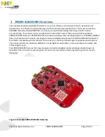
FRDM-K20D50MUM
Page 9 of 17
5.1.2
Serial and Debug Adapter (OpenSDA)
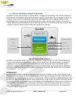
OpenSDA is an open-standard serial and debug adapter. It bridges serial and debug communications between a
USB host and an embedded target processor as shown in Figure 4. The hardware circuit is based on a Freescale
Kinetis K20 family microcontroller (MCU) with 128 KB of embedded flash and an integrated USB controller.
OpenSDA features a mass storage device (MSD) bootloader, which provides a quick and easy mechanism for
loading different OpenSDA Applications such as flash programmers, run-control debug interfaces, serial-to-USB
converters, and more. Refer to the
OpenSDA User’s Guide
for more details.
OpenSDA High-Level Block Diagram
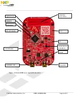
OpenSDA is managed by another Kinetis K20 MCU built on the ARM® Cortex™-M4 core. The OpenSDA circuit
includes a status LED (D4) and a pushbutton (SW1). The pushbutton asserts the Reset signal to the K20D128
target MCU. It can also be used to place the OpenSDA circuit into Bootloader mode. SPI and GPIO signals
provide an interface to either the SWD debug port of the K20. Additionally, signal connections are available to
implement a UART serial channel. The OpenSDA circuit receives power when the USB connector J7 is plugged
into a USB host.
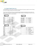
Debug Interface
Signals with SPI and GPIO capability are used to connect directly to the SWD of the K20. These signals are also
brought out to a standard 10-pin (0.05”) Cortex Debug connector (J6). It is possible to isolate the K20 MCU from
the OpenSDA circuit and use J6 to connect to an off-board MCU. To Signals with SPI and GPIO capability are used
to connect directly to the SWD of the K20. These signals are also brought out to a standard 10-pin (0.05”) Cortex
Debug connector (J6). It is possible to isolate the K20 MCU from the OpenSDA circuit and use J6 to connect to an
off-board MCU. To accomplish this, cut the trace on the bottom side of the PCB that connects J11 pin 1 to J11
pin 2. This will disconnect the SWD_CLK pin to the K20 so that it will not interfere with the communications to
an off-board MCU connected to J6.