


NXP Semiconductors
KTFRDMHB2001FEVMUG
FRDM-HB2001FEVM evaluation board
KTFRDMHB2001FEVMUG
All information provided in this document is subject to legal disclaimers.
© NXP B.V. 2016. All rights reserved
User guide
Rev. 1.0 — 25 May 2016
13 / 35
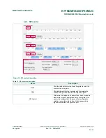
Output name
Description
CFB
Current mirror output for real time load current monitoring
MISO
Master input slave output for SPI
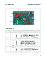
4.4.5 Test point definitions
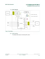
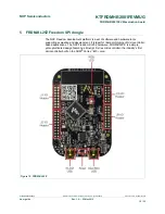
The following test points provide access to various signals to and from the board.
GND1
ENBL1
CCP
MISO1
CFB_V
VDD1
GND
IN_2
DIS1 IN_1
FS_B1
MOSI1
VPWR
SCLK1
GND2
CS_B1
GND3
VDDQ1
Figure 8. Test point locations
Table 7. Test point definitions
Test point name
Signal name
Description
CFB_V
CFB_READ
CFB pin voltage going to ADC
CCP
CCP
Charge pump voltage
ENBL1
ENBL
Enable/disable signal to activate/tri-
state the outputs and put the device to
Sleep mode
DIS1
DIS
Enable/disable signal to activate/tri-
state the outputs
IN_1
IN1
Direction control in H-Bridge mode and
OUT1 control in Half-Bridge mode
IN_2
IN2
PWM control in H-Bridge mode and
OUT2 control in Half-Bridge mode
VPWR
VPWR
System voltage
VDDQ1
VDDQ
VDDQ digital output supply voltage