background image

Copyright © 2010 NEXCOM International Co., Ltd. All Rights Reserved.

67

NSA 3111 User Manual

Appendix D: Power Consumption

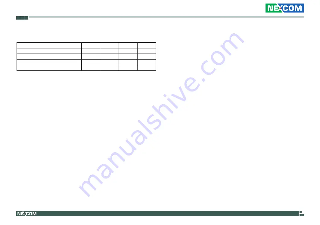
Total Power Requirements

Power Type

+12V

+5V

+3.3V

Total

Consumed watts (Item W)

148.8

94.5

44.8

288.18

Consumed currents (Item A )

12.4

18.9

13.6

Actually required currents  (Item A / 0.8)

15.5

23.6

17

Maximum BTU (Power Supply Watt * 3.412)

984 BTU/hr

Summary of Contents for NSA 3111 Series

Page 1: ...NEXCOM International Co Ltd NEXCOM International Co Ltd Published August 2010 www nexcom com Network and Communication Solutions Network Security Appliance NSA 3111 User Manual ...

Page 2: ...nts xii Ordering Information xiii Chapter 1 Product Introduction Overview 1 Key Features 1 Hardware Specifications 2 NSA 3111 System 2 Main Board NSB 3111 4 Getting to Know NSA 3111 7 Front Panel 7 Rear Panel 8 Chapter 2 Jumpers And Connectors Before You Begin 9 Precautions 9 Jumper Settings 10 Jumpers 11 RTC Clear 11 Power Type Select 11 Console Type Select 12 CF Card Master Slave Select 12 Conne...

Page 3: ...Setup 40 When to Configure the BIOS 40 Entering Setup 41 BIOS Main Menu 41 Getting Help 42 Using the Control Keys 43 BIOS Setup Utility 44 Standard CMOS Features 44 Advanced BIOS Features 47 Integrated Peripherals 49 Power Management Setup 53 PnP PCI Configurations 55 PC Health Status 56 Load Optimized Defaults 56 Set Password 57 Save Exit Setup 57 Exit Without Saving 58 Appendix A Watchdog Timer ...

Page 4: ...es if it has a CE marking For computer systems to remain CE compliant only CE compliant parts may be used Maintaining CE compliance also requires proper cable and cabling techniques Copyright This publication including all photographs illustrations and software is protected under international copyright laws with all rights reserved No part of this manual may be reproduced copied translated or tra...

Page 5: ...Polybrominated diphenyl Ethers PBDE 0 1 or 1 000ppm In order to meet the RoHS compliant directives NEXCOM has established an engineering and manufacturing task force in to implement the introduction of green products The task force will ensure that we follow the standard NEXCOM development procedure and that all the new RoHS components and new manufacturing processes maintain the highest industry ...

Page 6: ...ot responsible for the devices parts Customers are responsible for the safe packaging of defective products making sure it is durable enough to be resistant against further damage and deterioration during transportation In case of damages occurred during transportation the repair is treated as Out of Warranty Any products returned by NEXCOM to other locations besides the cus tomers site will bear ...

Page 7: ... uses parts specified by the manufacturer Avoid using the system near water in direct sunlight or near a heating device The load of the system unit does not solely rely for support from the rackmounts located on the sides Firm support from the bottom is highly necessary in order to provide balance stability The computer is provided with a battery powered real time clock circuit There is a danger o...

Page 8: ...greater than the voltage and current rating marked on the product 11 All cautions and warnings on the equipment should be noted 12 If the equipment is not used for a long time disconnect it from the power source to avoid damage by transient overvoltage 13 Never pour any liquid into an opening This may cause fire or electri cal shock 14 Never open the equipment For safety reasons the equipment shou...

Page 9: ...site at www nexcom com 2 For technical issues that require contacting our technical support team or sales representative please have the following information ready before calling Product name and serial number Detailed information of the peripheral devices Detailed information of the installed software operating system version application software etc A complete description of the problem The exa...

Page 10: ...17 Rue des entrepreneurs 78420 Carrières sur Seine France Tel 33 0 1 71 51 10 20 Fax 33 0 1 71 51 10 21 http www nexcom eu Global Service Contact Information Germany Leopoldstrase Business Centre Leopoldstrase 244 80807 Munich Germany Tel 49 89 208039 278 Fax 49 89 208039 279 http www nexcom eu Italy Via Gaudenzio Ferrari 29 21047 Saronno VA Italia Tel 39 02 9628 0333 Fax 39 02 9619 8846 http www ...

Page 11: ...a Tel 86 10 5885 6655 Fax 86 10 5885 1066 http www nexcom cn China Shanghai Office Room 1505 Greenland He Chuang Building No 450 Caoyang Rd Shanghai 200063 China Tel 86 21 6150 8008 Fax 86 21 3251 6358 http www nexcom cn China Nanjing Office Room 1206 Hongde Building No 20 Yunnan Rd Nanjing 210018 China Tel 86 25 8324 9606 Fax 86 25 8324 9685 http www nexcom cn China Shenzhen Office Western Room 7...

Page 12: ...S SYMBOL 1 5 6012200053X00 PE ZIPPER BAG 3 100x70mm W China RoHS SYMBOL 1 6 6023309081X00 CABLE EDI 232091081804 RS COM PORT DB9 FEMALE TO RJ45 8P8C L 1800mm 1 7 60233PS203X00 EBC563IO PS2 KB MS CABLE EDI 201061080201 RS PS2 TO JST 8PIN 2 54mm L 200mm 10mm 1 8 6029900037X00 DOW CORNING 340 Silcone Heat Sink Compound 3g 1 9 60233VGA25X00 VGA CABLE CONNTEK A02 C018 V01 VGA PORT TO HOUSING 2x8 PIT 2 ...

Page 13: ...S00311101X0 Supports Intel Core 2 Duo Pentium Dual Core Celeron 2 DDR2 memory slots 6 Gigabit LAN ports Compactflash socket VGA USB port One PCI Expansion slot One LAN Modular support optional NSA 3111 C4 P N 10S00311100X0 Supports Intel Core 2 Duo Pentium Dual Core Celeron 2 DDR2 memory slots 4 Gigabit LAN ports Compactflash socket VGA USB port One PCI Expansion slot One LAN Modular support optio...

Page 14: ...6 1U Rackmount Network Platform Intel Core 2 Quad Core 2 Duo Pentium Dual Core Celeron with 800 1066 1333 MHz FSB and 1MB 2MB cache Two DIMM sockets support DDR2 800 Dual Channel with Non ECC memory maximum of 4GB Rear Six 10 100 1000 Copper LAN ports and 1 LAN module bay Intel G41 chipset One PCI expansion slot One Mini PCI expansion slot Two internal 2 5 HDD bays optional Front ...

Page 15: ...assis NSC3111 System Cooling Cooling Method Fixed 2 system fans at the rear of the chassis Ventilation Suction from the side and discharged to the back I O Interface Front Console port One RJ45 type USB port Two USB ports LAN module bay LAN port 6x RJ45 copper LAN ports Button 1x GPIO software button I O Interface Rear VGA port One 2x8 2 0 mm box header connected to the VGA port located at the rea...

Page 16: ...5V 5V 12V 12V 3 3V 5VSB Maximum output power Up to 200W Environment Operating temperature 0o C 40o C Storage temperature 20o C 75o C Relative humidity 10 90 non condensing Vibration Sine wave vibration test non operating Frequency 5 500 Hz Acceleration 2g Random vibration test operating Frequency 5 500 Hz Acceleration 0 3g Random vibration test packing Frequency 1 200 Hz Acceleration 1 15g Shock N...

Page 17: ...logy DDR2 800MHz Non ECC memory Sockets Two 240 pin DDR2 DIMM sockets Capacity 4GB maximum memory Graphics Controller G41 integrated VGA controller Interface CRT port resolution up to 1024x768 60Hz box header 2x8 2 0mm Network Controller Intel 82574L x6 6 ports connected from ICH7R via PCI E x1 Link speed 10 100 1000 Media type Intel 82574 ports are copper RJ45 x6 ports Left Activity LED blinks Ye...

Page 18: ...tificates etc I O Port Internal I O PS 2 keyboard mouse one 2x4 2 54mm pin header Serial port one reserved 2x5 2 0mm box header COM2 USB port two USB connectors Digital I O GPIO from Super IO 2x5 GND and 5V 2 0mm 4 in 4 out pin header Rear I O One PCI expansion Front I O Two USB ports One RJ45 type console port One GPIO software button Six RJ45 copper LAN ports One LAN module bay optional Expansio...

Page 19: ...el 2 6 Fedora Core SUSE Drivers VGA LAN WDT GPIO Hardware Monitor Bypass Sample code LCM sample string display LCM testing program GPIO WTD Bypass Hardware Monitor Environment Operating temperature 0o C 40o C Storage temperature 20o C 75o C Relative humidity 10 90 non condensing EMI EMC CE FCC Class A ESD 2 4KV contact discharge 2 4 8KV air discharge Criteria B ...

Page 20: ...ftware button Console Port Used to connect RJ45 type Console device USB Ports Used to connect USB 2 0 1 1 devices Power LED Indicates the power status of the system HDD LED Indicates the status of the hard drive LAN Bypass Status LEDs Indicates the status of the LAN Bypass Copper LAN Ports Used to connect LAN network devices LAN Module Bay Used for installing a LAN module Front Panel Copper LAN po...

Page 21: ...1 User Manual Chapter 1 Product Introduction Expansion slot Power switch Power On Off Switch Press to power on or power off the system Expansion Slot Used to install expansion cards System Fans Cooling fans to dissipate heat from the system Rear Panel System fan System fan ...

Page 22: ... touching any internal components by touching a metal object Static electricity can damage many of the elec tronic components Humid environment tend to have less static electric ity than dry environments A grounding strap is warranted whenever danger of static electricity exists Precautions Computer components and electronic circuit boards can be damaged by discharges of static electricity Working...

Page 23: ...ing the jumpers ensure that the jumper caps are placed on the correct pins When the jumper cap is placed on both pins the jumper is short If you remove the jumper cap or place the jumper cap on just one pin the jumper is open Refer to the illustrations below for examples of what the 2 pin and 3 pin jumpers look like when they are short on and open off Two Pin Jumpers Open Left and Short Right Thre...

Page 24: ...RTC Clear Connector size 1x3 3 pin header 2 54 mm pitch Connector location JP1 1 3 Pin Settings 1 2 On Normal 2 3 On CMOS Clear 1 2 On default Pin Definition 1 Battery 3 3V 2 RTCRST 3 GND Power Type Select Connector size 1x3 3 pin header 2 54 mm pitch Connector location JP2 1 3 Pin Definition 1 2 On ATX 2 3 On AT 2 3 On default ...

Page 25: ...nual Console Type Select Connector size 1x3 3 pin header 2 54 mm pitch Connector location JP3 1 3 Pin Definition 1 2 On RTS to CTS 2 3 On Normal 2 3 On default CF Card Master Slave Select Connector size 1x3 3 pin header 2 54 mm pitch Connector location JP3 1 3 Pin Definition 1 2 On Master 2 3 On Slave 1 2 On default ...

Page 26: ...Manual External I O Interface Front Connector Pin Definitions RJ45 Type Console Port Connector type RJ45 port Connector location LAN1 Pin Definition Pin Definition 1 RTS CTS 2 DTR 3 TXD 4 GND 5 DCD 6 RXD 7 DSR 8 CTS GPIO Software Button Connector type 2 pin jack Connector location SW1 Pin Definition 1 GND 2 GPI12 ...

Page 27: ...1 User Manual Status Indicators Connector location LED1 Status LED Color PWR Green HDD Yellow Bypass B1 Yellow Bypass B2 Yellow Bypass B2 Bypass B1 PWR HDD USB Ports Connector type Dual USB port Connector location USB1 Pin Definition Pin Definition 1 P5V 5 P5V 2 USB1_N 6 USB2_N 3 USB1_P 7 USB2_P 4 GND 8 GND ...

Page 28: ...111 User Manual Copper LAN Ports Connector type RJ45 port with LEDs Connector location CON1 Act Link Act Status Yellow Blinking Data Activity Off No Acitivity Link Status Green Always Lighted 1G and 10 100MB Off No link Pin Definition Pin Definition 1 TX 0 2 TX 0 3 TX 1 4 TX 2 5 TX 2 6 TX 1 7 TX 3 8 TX 3 ...

Page 29: ...nd Connectors NSA 3111 User Manual Internal Connectors Reset Button Connector type 1x2 2 pin header 2 54 mm pitch Connector location J3 1 2 Pin Definition 1 GND 2 RESET Power Button Connector type 1x2 2 pin header 2 54 mm pitch Connector location J4 1 2 Pin Definition 1 GND 2 FP_SW_ON_N ...

Page 30: ... 2 0 mm pitch Connector location CN1 1 2 15 16 Pin Definition Pin Definition 1 RED 2 GREEN 3 BLUE 4 NC 5 GND 6 GND 7 GND 8 GND 9 P5V 10 GND 11 NC 12 VGADATA 13 HSYNC 14 VSYNC 15 VGACLK 16 NC PS 2 Keyboard Mouse Connector Connector type 2x4 8 pin header 2 54 mm Connector location J2 1 2 7 8 Pin Definition Pin Definition 1 P5V 2 P5V 3 KDAT 4 MDAT 5 KCLK 6 MCLK 7 GND 8 GND ...

Page 31: ...ctor Connector type 2x5 10 pin boxed header 2 0 mm Connector location CN2 1 2 9 10 Pin Definition Pin Definition 1 DCD2 2 RXD2 3 TXD2 4 DTR2 5 GND 6 DSR2 7 RTS2 8 CTS2 9 RI2 10 GND SATAII Ports Connector type Standard Serial ATAII 1 27mm Connector location J8 and J9 Pin Definition 1 GND 2 TXP0 3 TXN0 4 GND 5 RXN0 6 RXP0 7 GND 1 7 ...

Page 32: ...nnector Connector type 2x5 10 pin header 2 0 mm Connector location J7 10 9 2 1 Pin Definition Pin Definition 1 P5V 2 GND 3 GPI20 4 GPO24 5 GPI21 6 GPO25 7 GPI22 8 GPO26 9 GPI23 10 GPO27 USB Connector Connector type 1x6 6 pin boxed header 2 0 mm JST Connector location J1 1 6 Pin Definition 1 P5V 2 USB2 3 USB2 4 USB3 5 USB3 6 GND ...

Page 33: ...s and Connectors NSA 3111 User Manual Chip Fan Connector type 3 pin Wafer 2 54 mm pitch Connector location FAN1 Pin Definition 1 GND 2 12V 3 FAN_TAC System Fans Connector size 4 pin Wafer 2 54 mm pitch Connector location CN3 and CN4 1 3 1 4 Pin Definition 1 GND 2 12V 3 FAN_TAC 4 PWM ...

Page 34: ...hapter 2 Jumpers and Connectors NSA 3111 User Manual DIMM Sockets Connector type 240 pin DDR2 Connector location DIMM1 DIMM2 DIMM 2 DIMM 1 DIMM 2 Channel B DIMM 1 Channel A Always populate DIMM1 first The system will not boot when the first module is installed in DIMM2 ...

Page 35: ... 3 SDD4A 4 SDD5A 5 SDD6A 6 SDD7A 7 SDCS 1 8 GND 9 GND 10 GND 11 GND 12 GND 13 P5V 14 GND 15 GND 16 GND 17 GND 18 SDA2A 19 SDA1A 20 SDA0A 21 SDD0A 22 SDD1A 23 SDD2A 24 NC 25 CF_CD2 26 CF_CD1 27 SDD11A 28 SDD12A Pin Description Pin Description 29 SDD13A 30 SDD14A 31 SDD15A 32 SDCS 3 33 NC 34 SDIOR 35 SDIOW 36 P5V 37 HDIRQ14 38 P5V 39 CF_SEL 40 NC 41 IDERST 42 SIORDY 43 SDREQ 44 SDDACK 45 IDEACTP 46 ...

Page 36: ...Copyright 2010 NEXCOM International Co Ltd All Rights Reserved 23 Chapter 2 Jumpers and Connectors NSA 3111 User Manual Block Diagram of the Main Board ...

Page 37: ...r backward then remove it from the chassis Prior to removing the chassis cover make sure the unit s power is off and disconnected from the power sources to prevent electric shock or system damage 1 The screws around the cover are used to secure the cover to the chas sis Remove these screws and put them in a safe place for later use The dots denote the locations of the screws ...

Page 38: ...g a DIMM 1 The 2 DDR2 sockets are divided into 2 channels DIMM1 Channel A DIMM2 Channel B Always populate DIMM1 first The system will not boot when the first module is installed in DIMM2 2 Push the ejector tabs which are at the ends of the socket outward This indicates that the socket is unlocked Ejector tab DIMM2 DIMM1 ...

Page 39: ...e socket so that the notch on the module is aligned with the key on the socket The key ensures the module can be plugged into the socket in only one direction Notch on the module Key on the socket 4 Seat the module vertically pressing it down firmly until it is completely seated in the socket The ejector tabs at the ends of the socket will au tomatically snap into the locked position to hold the m...

Page 40: ...r cables are unplugged before you install the CPU The CPU socket must not come in contact with anything other than the CPU Avoid unnecessary exposure Remove the protec tive cap only when you are about to install the CPU CPU socket 1 If the system came with the heat sink already installed loosen the mounting screws that secure the heat sink to the board 2 Unlock the socket by pushing the load lever...

Page 41: ...Copyright 2010 NEXCOM International Co Ltd All Rights Reserved 28 Chapter 3 System Setup NSA 3111 User Manual Retention tab 3 Lift the load lever Load lever lifted 4 Lift the load plate Load plate ...

Page 42: ...th pin 1 of the CPU socket Handle the CPU by its edges and avoid touching the pins Gold mark on the CPU Pin 1 of the socket 6 Insert the CPU into the socket until it is seated in place The CPU will fit in only one orientation and can easily be inserted without exerting any force Do not force the CPU into the socket Forcing the CPU into the socket may bend the pins and damage the CPU ...

Page 43: ...e CPU is in place close the load plate then push the lever down until it snaps into the retention tab Load lever Load plate 8 Apply thermal paste on top of the CPU Do not spread the paste all over the surface When you later place the heat sink on top of the CPU the compound will disperse evenly Thermal paste on the CPU ...

Page 44: ...pter 3 System Setup NSA 3111 User Manual 9 The mounting holes around the CPU socket are used to mount the heat sink Align the mounting screws of the heat sink with the mounting holes around the CPU socket Tighten the screws to secure the heat sink in place Mounting hole ...

Page 45: ... Reserved 32 Chapter 3 System Setup NSA 3111 User Manual Installing a CompactFlash Card 2 With the CompactFlash card s label facing up position the card to the socket CompactFlash socket CompactFlash card 1 Locate for the CompactFlash socket on the board ...

Page 46: ...Copyright 2010 NEXCOM International Co Ltd All Rights Reserved 33 Chapter 3 System Setup NSA 3111 User Manual 3 Insert the card until it is completely seated in the socket ...

Page 47: ...rew 1 Remove the mounting screws that secure the drive bay to the chassis Mounting screw 2 Place the SATA hard drive onto the drive bay Align the mounting holes that are on the sides of the SATA drive with the mounting holes on the drive bay Use the provided mounting screws to secure the SATA drive in place Drive bay Connector side of SATA drive Mounting screw ...

Page 48: ...ights Reserved 35 Chapter 3 System Setup NSA 3111 User Manual 3 Align the mounting holes of the drive bay with the mounting studs on the chassis 4 Connect the SATA power cable and the SATA data cable to the SATA drive SATA power cable SATA data cable ...

Page 49: ...pyright 2010 NEXCOM International Co Ltd All Rights Reserved 36 Chapter 3 System Setup NSA 3111 User Manual 5 Use the mounting screws you removed in step 1 to secure the drive bay in place Mounting screw ...

Page 50: ...ghts Reserved 37 Chapter 3 System Setup NSA 3111 User Manual Installing a PCI Card 2 Remove the mounting screws that secure the L shaped bracket to the chassis 1 The PCI slot is attached on an L shaped bracket PCI slot L shaped bracket Mounting screw ...

Page 51: ...Rights Reserved 38 Chapter 3 System Setup NSA 3111 User Manual 3 Remove the slot cover s mounting screw Mounting screw Slot cover PCI slot 4 Align the PCI card with the PCI slot then push it firmly until it is com pletely seated in the slot PCI card ...

Page 52: ... Rights Reserved 39 Chapter 3 System Setup NSA 3111 User Manual 5 Secure the card with the screw you removed in step 3 Mounting screw 6 Install the bracket back into the chassis then secure the bracket with the mounting screws you removed in step 2 ...

Page 53: ...ed with the values found in CMOS With easy to use pull down menus you can configure such items as Hard drives diskette drives and peripherals Video display type and display options Password protection from unauthorized use Power management features The settings made in the setup program intimately affect how the com puter performs It is important therefore first to try to understand all the Setup ...

Page 54: ...el allows you to enter Setup Another way to enter Setup is to power on the computer and wait for the following message during the POST TO ENTER SETUP BEFORE BOOT PRESS CTRL ALT ESC Press the Del key to enter Setup BIOS Main Menu Once you enter Award BIOS CMOS Setup Utility the Main Menu will ap pear on screen The main menu allows you to select from several setup functions and two exit choices Use ...

Page 55: ...s Displays CPU System Temperature Fan Speed and System Voltages Value Load Optimized Defaults Use this menu to load the BIOS default values that is factory settings for optimum system per formance While Award has designed the custom BIOS to maximize performance the factory has the option to change these defaults to meet their needs Set Password Enables you to change set or disable the supervi sor ...

Page 56: ... Main Menu Enter Key Select or Accept an Item PgUp plus key Increase the numeric value or make changes PgDn minus key Decrease the numeric value or make changes F1 key General help only for Status Page Setup Menu and Option Page Setup Menu Use This Key To Do This F2 Shift F2 key Change color from total 16 colors F2 to select color forward Shift F2 to select color backward F5 key Restore the previo...

Page 57: ...inute second The time is based on the 24 hour military time clock For example 1 p m is 13 00 00 Hour displays hours from 00 to 23 Minute displays minutes from 00 to 59 Second displays seconds from 00 to 59 IDE Channel 0 Master and IDE Channel 1 Slave To configure the IDE drives move the cursor to a field then press En ter The following screen will appear IDE HDD Auto Detection IDE Channel 0 Master...

Page 58: ...fied as the landing zone for the read write heads Sector This field displays the number sectors per track Video This field selects the type of video adapter used for the primary system monitor Although secondary monitors are supported you do not have to select the type The default setting is EGA VGA EGA VGA Enhanced Graphics Adapter Video Graphics Array For EGA VGA SVGA and PGA monitor adapters CG...

Page 59: ...he base memory is typically 512K for systems with 512K memory installed on the motherboard or 640K for systems with 640K or more memory installed on the motherboard Extended Memory Displays the amount of extended memory detected during boot up Total Memory Displays the total memory available in the system Model Name Displays the model name of the main board BIOS Version Displays the current BIOS v...

Page 60: ...us Values F7 Optimized Defaults Press Enter Enabled USB CDROM CDROM Hard Disk Setup Enabled 115200 Hard Disk Boot Priority This field is used to select the boot sequence of the hard drives Move the cursor to this field then press Enter Use the Up or Down arrow keys to select a device then press to move it up or to move it down the list Phoenix AwardBIOS CMOS Setup Utility Hard Disk Boot Priority I...

Page 61: ...en the system will prompt for the password everytime the system boots or only when you enter the BIOS setup Set the password in the Set Supervisor User Password submenu System The system will not boot and access to Setup will be denied unless the correct password is entered at the prompt Setup The system will boot but access to Setup will be denied unless the correct password is entered at the pro...

Page 62: ...owing screen will appear Phoenix AwardBIOS CMOS Setup Utility OnChip IDE Device Item Help Menu Level If your IDE hard drive supports block mode select Enabled for auto matic direction of the optimal number of block read writes per sector the drive can support Move Enter Select F1 General Help PU PD Value F10 Save ESC Exit F5 Previous Values F7 Optimized Defaults IDE HDD Block Mode On Chip Primary ...

Page 63: ...y set the system according to your hard disk drive s timing Mode 0 4 You can select a mode that matches your hard disk drive s tim ing Caution Do not use the wrong setting or you will have drive errors IDE Primary Secondary Master UDMA and IDE Primary Second ary Slave UDMA These fields allow you to set the Ultra DMA in use When Auto is selected the BIOS will select the best available option after ...

Page 64: ...ld will show P0 P2 is Primary meaning SATA 1 and SATA 3 are Primary Onboard Serial Port 1 and Onboard Serial Port 2 3F8 IRQ4 2F8 IRQ3 3E8 IRQ4 2E8 IRQ3 2E0 IRQ4 Allows you to manually select an I O address for the serial port Disabled Disables the serial port USB 1 0 Controller This field is used to enable or disable the Universal Host Controller Inter face USB 1 0 USB 2 0 Controller This field is...

Page 65: ...nal Co Ltd All Rights Reserved 52 NSA 3111 User Manual Chapter 4 BIOS Setup ByPass Mode After PWR ON The options are All Enable All Disable and By Segment ByPass Mode After PWR OFF The options are All Enable All Disable and By Segment ...

Page 66: ...card or a fixed alarm on the system real time clock Phoenix AwardBIOS CMOS Setup Utility Power Management Setup Item Help Menu Level Move Enter Select F1 General Help PU PD Value F10 Save ESC Exit F5 Previous Values F7 Optimized Defaults Power Supply Type PWRON After PWR Fail ACPI Function Soft Off by PWR BTTN AT On Enabled Instant Off Power Supply Type This field is used to select the type of pow...

Page 67: ...led or disabled if the power button is pushed and released in less than 4 sec the system enters the Suspend mode The purpose of this function is to prevent the system from powering off in case you accidentally hit or pushed the power button Push and release again in less than 4 sec to restore Pushing the power button for more than 4 seconds will power off the system Instant Off Pressing and then r...

Page 68: ...nfig ure all of the boot and Plug and Play compatible devices Auto ESCD The system will automatically detect the settings for you Manual Choose the specific IRQ resources in the IRQ Resources field IRQ Resources Set each system interrupt to either PCI Device or Reserved Phoenix AwardBIOS CMOS Setup Utility IRQ Resources Item Help Menu Level Move Enter Select F1 General Help PU PD Value F10 Save ES...

Page 69: ...lity Esc Quit F10 Save Exit Setup Select Item Time Date Hard Disk Type Standard CMOS Features Advanced BIOS Features Integrated Peripherals Power Management Setup PnP PCI Configurations This option opens a dialog box that lets you install optimized defaults for all appropriate items in the whole setup utility Press the Y key and then Enter to install the defaults Press the N key and then Enter if ...

Page 70: ...our password the only way to solve this problem is to discharge the CMOS memory by turning power off and placing a shunt jumper cap on the RTC Clear jumper to short pin 2 and pin 3 for five seconds then putting the shunt back to pin 1 and pin 2 Phoenix AwardBIOS CMOS Setup Utility Esc Quit F10 Save Exit Setup Select Item Time Date Hard Disk Type Standard CMOS Features Advanced BIOS Features Integr...

Page 71: ...lity with out recording any new values or changing old ones Phoenix AwardBIOS CMOS Setup Utility Esc Quit F10 Save Exit Setup Select Item Time Date Hard Disk Type Standard CMOS Features Advanced BIOS Features Integrated Peripherals Power Management Setup PnP PCI Configurations PC Health Status Load Optimized Defaults Set Password Save Exit Setup Exit Without Saving Quit Without Saving Y N N ...

Page 72: ...pin 89 will become active high level 5 CRF6 must be 0x0 Write another 0x00 to CRF6 timeout disable even though it is already 0x00 Clear the timeout status Write 0 to LD8 CRF7 4 pin 89 will fall at the same time CRFC6 Default 0x00 Watchdog Timer Time out Value Writing a non zero value to this register causes the counter to load the value to Watchdog Counter and start counting down If Bit 7 and Bit ...

Page 73: ...L 87H OUT DX AL OUT DX AL MOV AL 07H POINT TO LOGICAL DEVICE NUMBER REG OUT DX AL INC DX MOV AL 08H OUT DX AL SET UNITS MOV DX 2EH MOV AL 0F5H OUT DX AL INC DX IN AL DX AND AL NOT 8 SECEND MODE OUT DX AL SET TIME OUT VALUE MOV DX 2EH MOV AL 0F6H OUT DX AL MOV AL NUMBER OF TIME OUT VALUE IN SECENDS 0 255 INC DX OUT DX AL EXIT THE SIO CONFIGURATION MODE MOV DX 2EH MOV AL 0AAH OUT DX AL ...

Page 74: ...ide This appendix provides definitions for the four GPI O pins on NSA 3111 GPI O General Purpose Input Output pins are provided for custom system design The pin programmed as input mode GPI or output mode GPO depends on the configuration GPIO J7 Pin 3 Pin 5 Pin 7 Pin 9 Pin 4 Pin 6 Pin 8 Pin 10 GPIN10 GPIN11 GPIN12 GPIN13 GPOUT14 GPOUT15 GPOUT16 GPOUT17 ...

Page 75: ...tion out 2eh 30h out 2fh 01h CRF0 GP10 GP17 I O selection register Default 0xFF When set to a 1 respective GPIO port is programmed as an input port When set to a 0 respective GPIO port is programmed as an output port out 2eh 0f0h out 2fh f0h GPIO10 13 as output pin GPIO14 17 as input pin CRF1 GP10 GP17 data register Default 0x00 If a port is programmed to be an output port then its respective bit ...

Page 76: ...yright 2010 NEXCOM International Co Ltd All Rights Reserved 63 Appendix B GPI O Programming Guide NSA 3111 User Manual SW1 Read GPI12 Sample Code mov dx 48Dh in al dx and al 10h now al bit4 is GPIO12 value ...

Page 77: ...ter 0XF2 Bit 7 Bit 6 Bit 5 Bit 4 Bit 3 Bit 2 Bit 1 Bit 0 R X X X X W W W Bit 7 Timer Expired 0 Timer has not expired 1 Timer has expired Bit 2 0 Timer Value 000 0 second 001 1 second 010 2 second 011 4 second 100 8 second 101 16 second 110 32 second 111 64 second Bypass Control Function BCSR Bypass Control Status Register 0XF3 Bit 7 Bit 6 Bit 5 Bit 4 Bit 3 Bit 2 Bit 1 Bit 0 W W R W R W R W R W R W...

Page 78: ...t 3 Bit 2 Bit 1 Bit 0 X X W W W W W W Bit 0 Segment 1 facing the front panel the leftmost is the 1st Bypass Bit 1 Segment 2 facing the front panel the second from the left is the 2nd Bypass Bit 2 Segment 3 facing the front panel the third from the left is the 3rd Bypass Bit 3 Segment 4 facing the front panel the fourth from the left is the 4th Bypass 0 Set segment bypass Disable when power off 1 S...

Page 79: ...B_VTT P1V8_SM P0V75_SM VTT P1V05_ICH P1V5 CPU 70 5 8 G41 0 1 22 1 6 ICH7 R 0 02 0 7 0 01 0 58 1 4 2 DDR2 6 1 2 CK505 0 55 Clock Buffer 0 5 82574L x 6 1 62 Relay x 16 1 6 PS2 KB MS 0 5 FAN x 4 1 5 USB x 4 2 Mini PCI Slot 0 02 0 4 0 6 PCI Slot 0 5 0 1 0 02 5 7 6 Total Current 2 0 1 0 02 0 74 9 51 11 6 70 22 5 8 7 6 1 2 1 4 2 A Mini PCI Add in card must limit its total power consumption to 2 Watts fr...

Page 80: ...User Manual Appendix D Power Consumption Total Power Requirements Power Type 12V 5V 3 3V Total Consumed watts Item W 148 8 94 5 44 8 288 18 Consumed currents Item A 12 4 18 9 13 6 Actually required currents Item A 0 8 15 5 23 6 17 Maximum BTU Power Supply Watt 3 412 984 BTU hr ...

Reviews: