DDC Interface
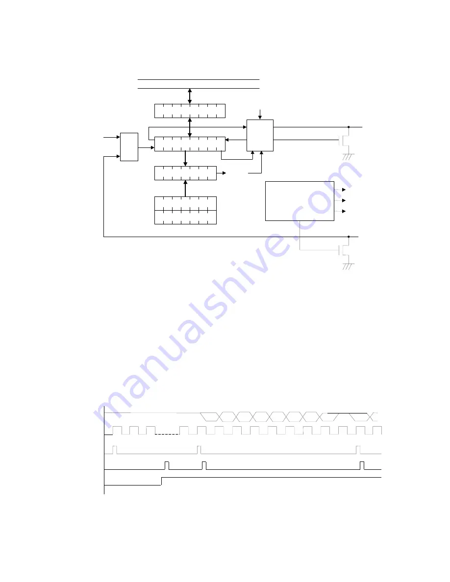
The DDC interface is a slave mode I
²
C interface with DDC1 function. It is fully compatible with VESA
DDC1/2B standard. The functional block diagram is shown in the below.
Data Buffer
Shift Register
Address Compare
1
Address Register
0 1 0 0 0 0
MUX
MUX
ENACK
ADDR
R/W
VSYNC
MSB
Internal Data Bus
SDA
START/STOP Detect
Handshake Control
START
STOP
DDC2B
SCL
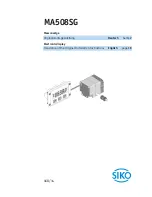
After power on or reset the DDC interface, it is in DDC1 state. The shift register shilfts out data to SDA pin
on the rising edge of VSYNC clock. Data format is an 8-bit byte followed by a null bit. Most significant bit
(MSB) is transmitted first. Every time when the ninth bit has been transmitted, the shift register will load a
data byte from data buffer (REG#18H). After loading data to the shift register, the data buffer becomes
empty and generates and INT0 interrupt. So the program must write one data byte into REG#18 every nine
VSYNC clocks.
Since the default values of data buffer (REG#22) and shift register are FFH, the SDA pin outputs high level
if no data had been written into data buffer after power on reset. When program finished initialization and set
the IEN_D bit to “1”, the INT0 will occur because the data buffer is empty. The INT0 service routine should
check the DDC2B bit is “0” and then writes the first EDID data byte into data buffer. When the second INT0
occurs, the INT0 service routine writes the second EDID data byte into data buffer and so on.
52
IEN_D
INT0
Load data to
shift register
Bit6
Bit5
Bit4
Bit3
Bit2
Bit1
Bit0
Bit7
SDA
Bit7
VSYNC
1
2
3
9
10
18
19
Summary of Contents for Diamand Scan 71
Page 9: ... 6 Diamand Scan 71 ...
Page 70: ...10 Monolithic triple 13 5nS CRT driver 67 ...
Page 71: ...68 ...
Page 72: ...69 ...
Page 73: ...70 ...
Page 102: ...99 SCHEMATIC DIAGRAMS 1 Video Board ...
Page 103: ...100 2 Main Board ...


