background image

13

LA000578A © 2006 Navman New Zealand. All rights reserved. 

Proprietary information and specifications subject to change without notice.

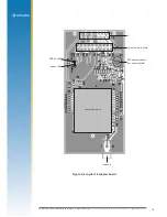
3.6 Jupiter 30 module on adapter board

Figure 3-6 (on the following page) shows the adapter board with the positions of the connectors 

and indicators.

Table 3-6 lists the pin configurations for the J1 and J2 connectors.

Jupiter function 

J2 (2.54 mm 

pitch header) 

pin no.

J1 (2 mm 

pitch header) 

pin no.

V_ANT

1

1

VCC_RF

2

V_BATT

3

3

VDD

4

4

M_RST

5

5

GPIO3/GYRO IN

6

6

GPIO15/FR

7

7

BOOT

8

8

GPIO1/W TICKS

9

9

RFON

10

GND

10

TXA

11

11

RXA

12

12

GPIO4

13

GND

13

TXB

14

14

RXB

15

15

Wake-up

16

GND

17

16

GPIO13

18

GND

17

GND

18

1PPS

19

19

GPS_FIX/GPIO10

20


Table 3-6 Connections J1 (2 mm pitch header) and J2 (2.54 mm pitch header)

4.0 Operating instructions

This section provides important information for the evaluation of the Jupiter 30 GPS module. 

Step-by-step instructions for connecting and operating the GPS development kit are included for 

first time setup. 

4.1 Initial connection and operation 

The following steps describe how to connect and operate the GPS Development Kit.

Install the supplied SiRFdemo on your PC:

1. Insert the supplied CD into the CDROM drive
2. Double click on the SiRFDemo software icon and follow the installation process. 

Set up the hardware:

1. Connect the DC power adapter to the power input J1.
2. Connect the antenna cable to the SMA coaxial antenna connector on the rear panel of the 

Development unit.

Summary of Contents for LA000578A

Page 1: ...upiter 30 20 channel GPS receiver module Development kit Guide AA003029 series Related products Jupiter 30 standard AA003025 G Related documents Jupiter 30 Data sheet LA000576 Jupiter 30 Product brief...

Page 2: ...h 3 BOOT from serial mode 8 3 2 4 DIP switch 4 GPIO1 W_TICKS input 8 3 2 5 DIP switch 5 RTC backup power enable 8 3 2 6 DIP switch 6 Antenna preamp power select 3 3 V or 5 12 V 8 3 2 7 DIP switch 7 An...

Page 3: ...on LEDs on front panel 9 Figure 3 6 Jupiter 30 adapter board 10 Figure 3 4 Pin layout of the clock out connector 11 Figure 4 1 Development unit test equipment 15 Tables Table 3 1 DIP switch settings 7...

Page 4: ...Windows based software presents the receiver s raw data in a geographical form allowing both detailed analysis and evaluation for both NMEA and SiRF Binary formats 2 0 Equipment This section provides...

Page 5: ...face cable A serial cable is provided to interface between the development unit and the customer s PC or between the development unit and a DGPS receiver This cable is terminated at both ends with fem...

Page 6: ...al of the DC power input at the rear of the unit will stop secondary power being applied assuming Jumper JB5 6 and switch 5 are correctly set Having this secondary power supply applied means that the...

Page 7: ...ACKUP POWER ON enabled 6 PREAMP power select OFF 3 V 7 PREAMP power select OFF 12 V 8 PREAMP power enable ON enabled These functions have been disabled by internal switch SW3 to allow correct operatio...

Page 8: ...the off position 3 2 6 DIP switch 6 Antenna preamp power select 3 3 V or 5 12 V Dip switch 6 provides control of the antenna preamp voltage applied to the module The switch position determines the sup...

Page 9: ...will begin flashing when the receiver is tracking a satellite 3 3 2 Power This LED indicates presence of primary DC power to the module 3 3 3 AUX This LED shows activity on the auxiliary serial RS232...

Page 10: ...rights reserved Proprietary information and specifications subject to change without notice Figure 3 6 Jupiter 30 adapter board Jupiter 30 module antenna power LED GPS fix LED J1 J2 not normally fitte...

Page 11: ...ary to open the unit Figure 3 5 illustrates the internal layout of the development unit board As shown in Figure 3 5 there is a selection of links that can be configured to provide functionality depen...

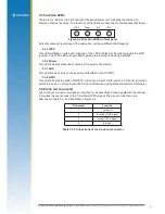
Page 12: ...nts are shown in Table 3 5 Test point Function E1 TXA E2 RXA E3 TXB E4 RXB E6 1PPS E7 not used E8 ground E9 ground Table 3 5 Signals available on the test points There are some settings that should no...

Page 13: ...6 GPIO13 18 GND 17 GND 18 1PPS 19 19 GPS_FIX GPIO10 20 Table 3 6 Connections J1 2 mm pitch header and J2 2 54 mm pitch header 4 0 Operating instructions This section provides important information for...

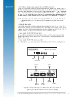
Page 14: ...S signals can reflect off metal or coated glass These reflections have a longer path than direct signals and can cause multi path errors 4 3 Connecting an RTCM differential source For debugging purpos...

Page 15: ...t the Settings Communications tab 3 When the Communications Settings window is displayed select the correct COM Port and set the Baud rate to 9600 Baud When this has been carried out and the developme...

Page 16: ...SiRF binary select the Action menu and click on the Switch to SiRF Protocol This should now present information in each window similar to that of VisualGPS Whilst enabled in SiRF binary protocol more...

Page 17: ...VMAN PRODUCTS INCLUDING LIABILITY OR WARRANTIES RELATING TO FITNESS FOR A PARTICULAR PURPOSE CONSEQUENTIAL OR INCIDENTAL DAMAGES MERCHANTABILITY OR INFRINGEMENT OF ANY PATENT COPYRIGHT OR OTHER INTELL...

Reviews: