background image

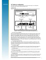
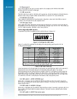
ON/OFF switch

configuration DIP


switch

function LEDS

JB5/6

reset switch

serial port 1

serial port 2

timing connector

DR connector

DC power

JB10/11/12

voltage selection  

switch (3.3V or 5V)

JB1/2

JB3/4

JB13/14/15

test points E1 to E9

JB16/17

SW3


all off except SW3.3

9

LA000510C © 2006 Navman NZ Ltd. All rights reserved. Proprietary information and specifications subject to change without notice.

3.4 Clock out connector

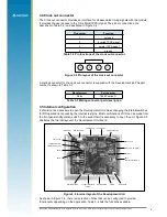
The Clock out connector provides an interface for all associated timing signals with the module. 

It provides the user access to the Time Mark (1PPS) signal. The pinout connections are 

described in Table 3-2, and illustrated in Figure 3-4.

Pin number

Function

1

not used

2

inverted 1PPS signal

3

normal 1PPS signal

4

ground

Table 3-2 Pin functions of the clock out connector

4

3

2

1

Figure 3-4 Pin layout of the clock out connector

A mating connector for the clock out connector is supplied with the Development kit. The part 

number is shown in Table 3-3.

Manufacturer

Part number

Molex

70400 series ‘G’

Table 3-3 Mating connector part description

3.5 Internal configuration

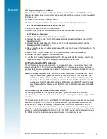
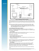
It should not be necessary to open the Development Unit unless changing the internal switches 

for DR operation or accessing the internal test pins. Most combinations of I/O can be made from 

the front panel configuration switch. In the event that it is necessary to open the unit, Figure 3-5 

illustrates the internal layout of the Development Unit board. 

Figure 3-5 Internal layout of the Development Unit 

As shown in Figure 3-5, there is a selection of links that can be configured to provide 

functionality depending on the application. Table 3-4 lists the functions available.

Summary of Contents for LA000507

Page 1: ...dead reckoning TU20 D421 201 Related documents Jupiter 20 Product brief LA000509 Jupiter 20 Data sheet LA000507 Jupiter 20 DR Application note LA000433 Jupiter 30 20 Integrator s manual LA000577 SiRF...

Page 2: ...DIP switch 6 Antenna preamp power select 3 3 V or 5 12 V 8 3 2 7 DIP switch 7 Antenna preamp power select 5 V or 12 V 8 3 2 8 DIP switch 8 Antenna preamp power enable 8 3 3 Function LEDs 8 3 3 1 1PPS...

Page 3: ...4 Pin layout of the clock out connector 9 Figure 3 5 Internal layout of the Development Unit 9 Figure 3 6 Jupiter 20 adapter board 11 Figure 4 1 Development Unit test equipment 13 Figure 5 1 DR interf...

Page 4: ...rce for SRAM and RTC Provision to insert a current measuring device to monitor both primary and backup power usage under various conditions Regulated DC power supply to the Jupiter 20 module Status in...

Page 5: ...alysis software are also provided to allow communication with the Jupiter 20 GPS receiver through a serial port This Windows based software presents the receiver s raw data in a geographical form allo...

Page 6: ...r of the unit will stop secondary power being applied assuming Jumper JB5 6 and switch 5 are correctly set Having this secondary power supply applied means that the Jupiter 20 will have a hot start ca...

Page 7: ...FR OFF high 3 Serial BOOT OFF normal run 4 GPIO1 W_TICKS OFF high 5 RTC BACKUP POWER ON enabled 6 PREAMP power select OFF 3 V 7 PREAMP power select OFF 12 V 8 PREAMP power enable ON enabled These fun...

Page 8: ...s of switches 7 and 8 also need to be considered when using the preamp function Note the supplied antenna is a 3 3 V type 3 2 7 DIP switch 7 Antenna preamp power select 5 V or 12 V DIP switch 7 also c...

Page 9: ...round Table 3 2 Pin functions of the clock out connector 4 3 2 1 Figure 3 4 Pin layout of the clock out connector A mating connector for the clock out connector is supplied with the Development kit Th...

Page 10: ...3 3 V supplied to Pin 1 of the DR connector JB13 14 not used JB14 15 not used JB16 17 Internal interface enable normally fitted Table 3 4 Pin functionality In addition to the configurable jumpers the...

Page 11: ...e connectors and indicators Figure 3 6 Jupiter 20 adapter board Table 3 6 lists the pin configurations for the J1 and J2 connectors Jupiter function J2 2 54 mm pitch header pin no J1 2 mm pitch header...

Page 12: ...a clear view of the sky for optimal reception of the satellite signals The 1PPS LED should begin flashing at 1 Hz once the receiver is powered and has started receiving at least one satellite This pro...

Page 13: ...ualGPS VisualGPS graphically presents the serial data transmitted by the receiver The receiver output must be enabled in the NMEA protocol for this software to be used To enable the receiver output 1...

Page 14: ...d now present information in each window similar to that of VisualGPS Whilst enabled in SiRF binary protocol more of the analysis software s functionality can be accessed To switch back into NMEA mode...

Page 15: ...normally at 0 V but rises to 3 V when the vehicle is in the reverse gear Use of this signal is optional if it is not used the effect of occasional reversing by the vehicle will not significantly degr...

Page 16: ...DUCTS INCLUDING LIABILITY OR WARRANTIES RELATING TO FITNESS FOR A PARTICULAR PURPOSE CONSEQUENTIAL OR INCIDENTAL DAMAGES MERCHANTABILITY OR INFRINGEMENT OF ANY PATENT COPYRIGHT OR OTHER INTELLECTUAL P...

Reviews: