


Evaluation Board of ML8088s Receiver
Operating Manual 2.0
25
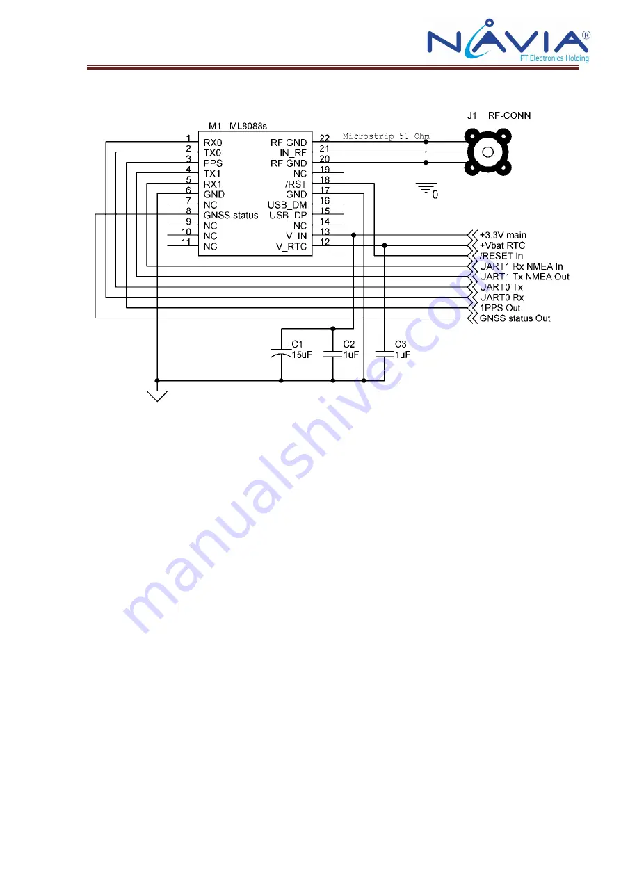
Typical connection circuit
Fig.23. Typical connection circuit for ML8088s chip.
Power supply V
dd
= 3,0…3,6V is provided to the 13 contact pad, as shown on the curcuit
as
+3.3V main. All the voltage values are measured relative to bus GND (common).
The voltage at any time on any pin of the receiver should not exceed 3,6V.
Voltage from the backup battery of RTC clock in the range V
bat
= 2,0…3,6 V should be
provided to contact pad 12 (V_RTC). This line is shown as the
+V
bat
RTC
on the connection
circuit graph. It is recommended to provide V
bat
voltage permanently to keep internal clock and
memory operational. In addition, backup battery provides power supply for the module firmware
activation register memory (module firmware). Not recommended to use backup battery with
voltage, exceeding the main power supply voltage level, which results in the current
overconsumption from the backup battery during the circuit operation.
During the first activation of the main power supply V
dd
after the connecting the battery
V
bat
the low logical level pulse should be sent obligatory to the pin 18 (IN/RST). This line is
shown as
/RESET In
on the graph. This is necessary for the correct selection of the built-in
microcontroller mode operation (operation or the firmware write to build-in flash memory), for
the firmware activation and write of its activation status to the register memory. The signal pulse
duration should at least 10 ms, the input voltage should not exceed 0,1 V and the load-carrying
capacity should be not less than 0.8 mA. During the further power supply connections V
dd
the
pulse signal to the pin IN/RST is not obligatory, due to the fact that this signal pulse erases the
current time information, that increases the the satellites search and registration time. The timing
chart for states and signal levels on the module pins during the connection of V
bat
and V
dd
is
given on Fig. 24
Note, that all the states and signals are measured relative to receiver module.
The voltage on the OUT pins at any time should NOT be the power source for the module
(so-called «phantom power supply»),, i.e. the voltage on the TxD0 (TX0), RxD0 (RX0), TxD1
(TX1) и RxD1 (RX1) pins should not exceed the main power voltage at any time. Obviously, the
voltage on the above mentioned pins should not present during the main power V
dd
disconnected
time, for example these pins are switched to high-impedance state «Z state», input mode or the


