background image

Y1

U1

U2

TP4

     GND

TP3

GND

  TP2

GND

 TP1

GND

VDD Set

VR1

J6

GND   TP5

TP7

VDD_IN

J3

J2

CLK

TP8

VIN

J5

National 

Semiconductor

ADC121S101 Evaluation Board

Rev. 1

J7

ADC121S101

ADC101S101

ADC081S101

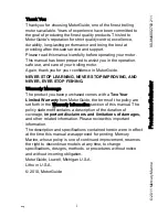
Figure 1. The Evaluation Board

4.0 Functional Description

is  2.7V  to  5.25V,  this  is  also  the  range  of  the  reference

voltage.

The ADC121S101 Evaluation Board component locations

are shown in 

Figure 1

. The board schematic is shown in

Figure 2

.

4.3 ADC clock circuit

The  clock  signal  applied  to  the  ADC  can  comes  from

BNC  J2  or  from  an  on-board  oscillator  at  position  Y1  or

Y2. Y1 is for a through-hole TTL oscillator, while Y2 is for

a  surface  mounted  TTL  oscillator.  Only  one  oscillator

should  be  mounted  at  a  time  and  either  an  oscillator  or

an external generator should be connected. When using

an external clock source, be sure that there is a 51 Ohm

resistor at position R2 near BNC J2. Resistor R2 should

be  removed  if  the  on-board  oscillator  is  used.  These

boards are shipped without R2 populated.

4.1 Input (signal conditioning) circuitry

The input signal to be digitized should be applied to BNC

connector J3  through  an  appropriate  filter.  This  50  Ohm

input is intended to accept a low-noise sine  wave  signal

of  peak-to-peak  amplitude  up  to  the  power  supply  level.

To  accurately  evaluate  the  ADC121S101  dynamic

performance,  the  input  test  signal  should  be  a  single

frequency passed through a high-quality band pass filter

as described in Section 5.0.

4.5 Digital Data Output.

The input signal may be either a.c. or d.c. coupled to the

ADC121S101  with  the  setting  of  the  jumper  on  J4.  See

schematic 

Figure 2

.

The digital output data from the ADC121S101 is available

at Header J7 for connection to a logic analyzer. Data is

transferred over FutureBus J5 for use with the

WaveVision data capture board.

4.2 The ADC reference

4.6 Power Supply Connections

The reference voltage for the ADC121S101 is the device

supply  voltage.  Therefore,  adjusting  this  voltage  will

change the full  scale  range  of  the  ADC121S101  .  Since

the operational supply voltage range of the ADC121S101

Power to this board is supplied through power connector

J6.  The  only  Voltage  needed  for  the  ADC121S101

evaluation board is a 2.7V to +5.6V supply.


5


http://www.national.com

Summary of Contents for ADC081S021

Page 1: ...1 ADC101S021 ADC081S021 50 ksps to 1 Msps 12 10 and 8 Bit Analog to Digital Converters Y1 U1 U2 TP4 GND TP3 GND TP2 GND TP1 GND VDD Set VR1 J6 GND TP5 TP7 VDD_IN J3 J2 CLK TP8 VIN J5 National Semiconductor ADC121S101 Evaluation Board Rev 1 J7 ADC121S101 ADC101S101 ADC081S101 2003 2004 2005 National Semiconductor Corporation 1 http www national com ...

Page 2: ... Blank Page 2 http www national com ...

Page 3: ...stalling and Using the ADC121S101 Evaluation Board 6 5 1 Software Installation 6 5 2 Setting up the ADC121S101 Evaluation Board 6 5 2 1 Board Set up 6 5 2 2 Quick Check of Analog Functions 6 5 2 3 Quick Check of Software and Computer Interface Operation 6 5 2 4 Getting Consistent Readings 7 5 2 5 Troubleshooting 7 6 0 Evaluation Board Specifications 7 7 0 Hardware Schematic 8 8 0 ADC121S101 Evalua...

Page 4: ...ard should be coupled to a WaveVision data capture board National part number WAVEVSN BRD 4 0 The WaveVision4 software that controls that board operates on Microsoft Windows The analog signal presented to the ADC121S101 is captured by the WaveVision4 data capture board and displayed on the computer screen as a dynamic waveform FFT and histogram The software also computes and displays SNR SINAD THD...

Page 5: ...ning circuitry The input signal to be digitized should be applied to BNC connector J3 through an appropriate filter This 50 Ohm input is intended to accept a low noise sine wave signal of peak to peak amplitude up to the power supply level To accurately evaluate the ADC121S101 dynamic performance the input test signal should be a single frequency passed through a high quality band pass filter as d...

Page 6: ... ADC121S101 power supply 3 Scope TP8 to be sure the input signal is present This completes the testing of the analog portion of the evaluation board 5 0 Installing and Using the ADC121S101 Evaluation Board 5 2 3 Quick Check of Software and Computer Interface Operation 1 Perform steps 1 through 3 of Paragraph 5 2 2 above The evaluation board requires a power supply as described in Section 4 7 An ap...

Page 7: ...that the ADC121S101 input signal does not go below ground or above the ADC121S101 supply voltage When we do this however we must be sure that the input signal has high spectral purity and stability and that the sampling clock signal is extremely stable with minimal jitter Coherent sampling of a periodic waveform occurs when an integer number of cycles exists in the sample window The relationship b...

Page 8: ...K K G K L K K M K N K K 7 K O K G P K G K G G K G L K G G L M N 7 O P G L M N 7 O G P G G G G L G G L M N 7 O P G L M N 7 O G P G G G G L G K G L M N 7 O P G L M N 7 O G P G G G G L G K G K L K K M K N K K 7 K O K P K K G K L K K M K N K K 7 K O K G P K G K G G K G L K G G L M N 7 O P G L M N 7 O G P G G G G L G G L M N 7 O P G L M N 7 O G P G G G G L G 3 4 5 5 4 5 4 4 G 4 4 2 0 0 F Power connecto...

Page 9: ...R3 R8 51 1 1 Type 0805 16 3 R4 R5 1K 5 Type 0805 17 2 R6 R9 10K 1 Type 0805 18 1 R7 100 Type 0805 19 1 TP1 TP2 TP3 TP4 TP5 TP6 TP7 TP8 TEST POINTS DigiKey S1012 36 ND 20 1 U1 ADC121S101CIMF or ADC101S101CIMF or ADC081S101CIMF or ADC121S051CIMF or ADC101S051CIMF or ADC081S051CIMF ADC121S021CIMF or ADC101S021CIMF or ADC081S021CIMF National Semiconductor 21 1 U2 24C02N Various 22 1 VR1 1K Potentiomet...

Page 10: ...c Analyzer Header 1 Ground 2 ADC Serial Data Output 3 ADC Serial Data Input 4 ADC Chip Select active low 5 ADC serial Clock J1 Clock Enable none Clock at Y1 or Y2 is disabled if oscillator has enable input 1 2 Clock at Y1 or Y2 is enabled J10 FutureBus Connector A1 B1 A2 B2 5V from WaveVision4 Capture Board D2 ADC Serial Clock B3 EEPROM SDA Data C3 EEPROM SCL Clock D3 EEPROM Power A4 ADC Data Outp...

Page 11: ... Blank Page 11 http www national com ...

Page 12: ... can be reasonably expected to result in a significant injury to the user 2 A critical component is any component in a life support device or system whose failure to perform can be reasonably expected to cause the failure of the life support device or system or to affect its safety or effectiveness National Semiconductor Corporation Americas Tel 1 800 272 9959 Fax 1 800 737 7018 Email support nsc ...

Reviews: