background image

Chapter 4

Theory of Operation

© National Instruments Corporation

4-3

SCXI-1122  User Manual

The major components of the SCXI-1122 are as follows:

The rear signal connector

The SCXIbus connector

The SCXIbus interface

The digital control circuitry

The analog circuitry

The SCXI-1122 consists of 16 isolated multiplexed channels with gains of 0.01, 0.02, 0.05, 0.1,
0.2, 0.5, 1, 2, 5, 10, 20, 50, 100, 200, 500, 1,000, and 2,000, and two isolated excitation channels
with voltage and current excitation.  The SCXI-1122 also has a digital section for automatic
control of channel scanning, temperature selection, gain selection, and filter selection.

The remainder of this chapter describes the theory of operation for each of these components.

Rear Signal Connector, SCXIbus Connector, and SCXIbus Interface

The SCXIbus controls the SCXI-1122.  The SCXIbus interface interfaces the signals of the rear
signal connector to the SCXIbus, allowing a DAQ board to control the SCXI-1122 and the rest of
the chassis.

Digital Control Circuitry

The digital control section consists of the Address Handler Register, the Configuration Register,
the Status Register, and the Module ID Register.  The Address Handler Register controls which
register is being addressed.  The Configuration Register configures the SCXI-1122 such as gain
selection, shunt calibration, filter bandwidth, two-wire or four-wire scanning, CJS selection, and
auto-zeroing.  The Status Register indicates if the SCXI-1122 is done configuring its internal
circuitry or is still in progress of doing so.  The Module ID Register contains the module ID A
hex, a code unique to the SCXI-1122.  You can read this module ID over the SCXIbus to
determine the type of module in a particular slot.

Analog Circuitry

The analog circuitry consists of a relay multiplexer, a software-programmable gain isolation
amplifier, software-programmable filtering, a temperature sensor channel for cold-junction
compensation, calibration hardware, and voltage and current excitation channel outputs.

Analog Input Channels

The relay multiplexer feeds into the isolation amplifier.  This relay multiplexer can be configured
in two-wire or four-wire mode scanning.  In two-wire scan mode all sixteen channels operate as
voltage sense channels.  At any point in time one and only one of sixteen channels is connected
to the isolation amplifier.  In the four-wire scan mode the sixteen channels are divided into two

Summary of Contents for SCXI -1122

Page 1: ...993 1999 National Instruments Corporation All Rights Reserved User Manual Sixteen Channel Isolated Transducer Multiplexer Module for Signal Conditioning September 1999 Edition Part Number 320516B 01 S...

Page 2: ...905 785 0085 Canada Qu bec 514 694 8521 China 0755 3904939 Denmark 45 76 26 00 Finland 09 725 725 11 France 01 48 14 24 24 Greece 30 1 42 96 427 Germany 089 741 31 30 Hong Kong 2645 3186 India 918052...

Page 3: ...AUSED BY FAULT OR NEGLIGENCE ON THE PART OF NATIONAL INSTRUMENTS SHALL BE LIMITED TO THE AMOUNT THERETOFORE PAID BY THE CUSTOMER NATIONAL INSTRUMENTS WILL NOT BE LIABLE FOR DAMAGES RESULTING FROM LOSS...

Page 4: ...ART OF THE USER OR APPLICATIONS DESIGNER ADVERSE FACTORS SUCH AS THESE ARE HEREAFTER COLLECTIVELY TERMED SYSTEM FAILURES ANY APPLICATION WHERE A SYSTEM FAILURE WOULD CREATE A RISK OF HARM TO PROPERTY...

Page 5: ...n 2 1 Digital Signal Connections 2 3 Analog Configuration 2 3 Current Loop Receivers 2 4 Hardware Installation 2 6 Chapter 3 Signal Connections 3 1 Front Connector 3 3 Front Signal Connection Descript...

Page 6: ...rview 5 1 Calibration Procedure 5 1 Calibration Equipment Requirements 5 1 Gain and Offset Calibration 5 2 Excitation Calibration 5 4 Appendix A Specifications A 1 Analog Input A 1 Excitation A 3 Phys...

Page 7: ...and Averaging Rather Than Single Sample Channel Scanning 3 8 Figure 3 7 Connecting a Quarter Bridge Strain Gauge to Channel 0 3 9 Figure 3 8 SCXI 1122 Rear Signal Connector Pin Assignments 3 10 Figure...

Page 8: ...scribes the optional software optional equipment and custom cables and explains how to unpack the SCXI 1122 Chapter 2 Configuration and Installation describes how to configure the SCXI 1122 jumpers an...

Page 9: ...ming examples and syntax examples This font is also used for the proper names of disk drives paths directories programs subprograms subroutines device names functions variables filenames and extension...

Page 10: ...t up your hardware system use either the application software LabVIEW or LabWindows manuals or the NI DAQ manuals to help you write your application If you have a large and complicated system it is wo...

Page 11: ...omments on our products and manuals We are interested in the applications you develop with our products and we want to help if you have problems with them To make it easy for you to contact us this ma...

Page 12: ...AQ board channel The SCXI 1122 operates with full functionality with the National Instruments MIO 16 Lab PC and the SCXI 1200 boards You can use the Lab and PC LPM 16 boards with the SCXI 1122 but the...

Page 13: ...tware LabWindows has two versions LabWindows for DOS is for use on PCs running DOS and LabWindows CVI is for use on PCs running Windows and Sun SPARCstations LabWindows CVI features interactive graphi...

Page 14: ...or Workstation Figure 1 1 The Relationship between the Programming Environment NI DAQ and Your Hardware The National Instruments PC AT and MC Series DAQ boards are packaged with NI DAQ software for P...

Page 15: ...ed the register level programmer manual The SCXI 1122 Register Level Programmer Manual contains low level programming details such as register maps bit descriptions and register programming hints that...

Page 16: ...manufacturer part number that National Instruments uses for this connector is as follows ERNI part number 913523 The mating connector for the SCXI 1122 front connector is a 48 pin DIN C female connec...

Page 17: ...ontains two jumpers that are shown in the parts locator diagram in Figure 2 1 Jumper W2 connects a pullup resistor to the SERDATOUT signal on the rear signal connector Jumper W1 configures the guard a...

Page 18: ...Configuration and Installation Chapter 2 SCXI 1122 User Manual 2 2 National Instruments Corporation Figure 2 1 SCXI 1122 Parts Locator Diagram...

Page 19: ...ter and the EEPROM National Instruments software does not read the Module ID automatically you must indicate to the software which module is in which slot An open collector driver a driver that active...

Page 20: ...connects the analog reference to the OUTREF pin on the rear signal connector Select this mode when the SCXI 1122 has to operate with DAQ boards that have a nonreferenced single ended NRSE input Do no...

Page 21: ...any installed module disconnect the AC power line or any high voltage sources 30 Vrms 42 4 Vpk or 60 Vdc that may be connected to the module To install the resistors you need to do the following befor...

Page 22: ...d attach the connector at the metal end of the SCXI 1340 cable assembly to the rear signal connector on the SCXI 1122 module Screw the rear panel to the rear threaded strip Attach the loose end of the...

Page 23: ...are connected to the module or terminal block dangerous voltages may exist even when the equipment is turned off Before you remove any installed terminal block or module disconnect the AC power line o...

Page 24: ...not connected to the chassis To connect the safety earth ground to the strain relief tab run an earth ground wire in the cable from the signal source to the terminal block National Instruments is NOT...

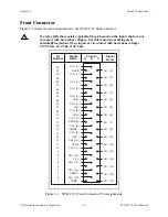
Page 25: ...uts as potentially hazardous if any inputs are in contact with hazardous voltages 30 Vrms 42 4 Vpk or 60 Vdc Pin Number Signal Name Column A B C Signal Name 32 31 30 29 28 27 26 25 24 23 22 21 20 19 1...

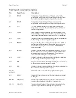
Page 26: ...tage Sense This pin must be tied to VEX at the load for remote sensing When using the SCXI 1322 terminal block this pin is connected to VEX SENSE screw terminals A17 SENSE Positive Voltage Sense This...

Page 27: ...ay inputs the temperature sensor output from the terminal block located on pins A3 TEMP and A1 TEMP is also connected to the amplifier input selector All inputs are fully isolated from earth ground an...

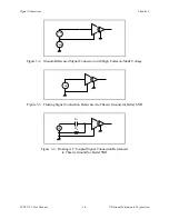
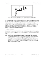
Page 28: ...poration Vs Vcm Figure 3 2 Ground Referenced Signal Connection with High Common Mode Voltage Vs Figure 3 3 Floating Signal Connection Referenced to Chassis Ground for Better SNR Vs Rb Cc Figure 3 4 Fl...

Page 29: ...ificant input offset may result To determine the maximum offset the biasing resistor will introduce use the following equation Vofsbias Ibias x Rbias The input signal range of an SCXI 1122 input chann...

Page 30: ...e VEX and a current IEX excitation channel which are available at the front connector In addition VEX 2 is available for half bridge and quarter bridge transducers Both channels are isolated from eart...

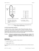
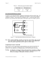
Page 31: ...ain Gauge VEX 120 Dummy Resistor Figure 3 7 Connecting a Quarter Bridge Strain Gauge to Channel 0 Note When using the half bridge completion network with a quarter bridge setup you must use an extra r...

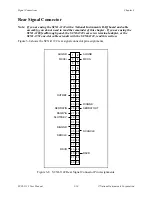
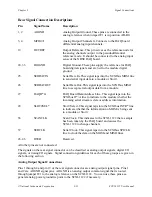
Page 32: ...h panel the SCXI 1343 rear screw terminal adapter or the SCXI 1351 one slot cable extender with the SCXI 1122 read this section Figure 3 8 shows the SCXI 1122 rear signal connector pin assignments 1 2...

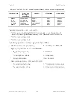
Page 33: ...This signal taps into the SCXIbus D A line to indicate to the module whether the incoming serial stream is data or address information 29 SLOT0SEL Slot 0 Select This signal taps into the SCXIbus INTR...

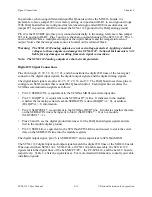
Page 34: ...put signals the digital output signals and the digital timing signals The digital input signals are pins 24 25 27 29 33 and 37 The DAQ board uses these pins to configure an SCXI module that is under D...

Page 35: ...I 1122 to increment to the next channel after each conversion by the DAQ board during scanning This signal is referred to as SCANCLK Pin 43 is a reserved digital input Pin 46 is a reserved digital inp...

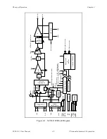
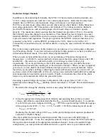
Page 36: ...eory of Operation This chapter contains a functional overview of the SCXI 1122 module and explains the operation of each functional unit making up the SCXI 1122 Functional Overview The block diagram i...

Page 37: ...or 1 AB0 Switch AB0 AB0 MCH0 MCH0 AB0 Control Attenuator Calibration EEPROM TEMP TEMP RSVD CH0 CH7 CH8 CH15 IEX IEX VEX R LPF and Protection Temp Auto Zero Protection Temp MIEX Mux Counter 8 Input Rel...

Page 38: ...ister the Status Register and the Module ID Register The Address Handler Register controls which register is being addressed The Configuration Register configures the SCXI 1122 such as gain selection...

Page 39: ...ake a large number of samples and average them To achieve 50 or 60 Hz rejection you should acquire data over an integral number of power line cycles then average this data The filtering consists of on...

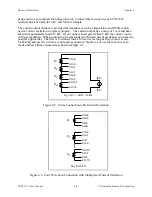
Page 40: ...tor is socketed to permit you to change its value to meet your requirements If you are performing several strain measurements you can enable the shunt calibration then proceed with scanning all of the...

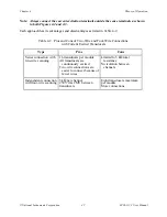
Page 41: ...loads greater than 5 k the current source will lose regulation When connecting several loads which need current excitation you have two possible approaches The first is to connect them all in series a...

Page 42: ...2 Pros and Cons of Two Wire and Four Wire Connections with Current Excited Transducers Type Pros Cons Series connection with two wire scanning 16 transducers per module All transducers are continuous...

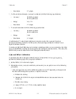
Page 43: ...ns for further details You can store this offset in the onboard EEPROM for future use and for automatic calibration when you are using National Instruments software The EEPROM also stores correction f...

Page 44: ...offset you can determine the offset errors of the DMM by shorting its leads together and reading the measured value This value the DMM offset must be subtracted from all subsequent measurements Gain a...

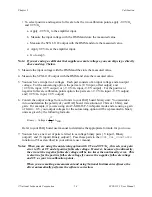
Page 45: ...Convert the output voltage from volt units to your DAQ board binary unit You must take into consideration the polarity of your DAQ board its resolution 12 bits or 16 bits and gain For example if you a...

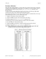
Page 46: ...load and measure the voltage 3 Pass this voltage to the SCXI_Cal_Constants function or VI To determine the current excitation calibration constants follow this procedure 1 Set your DMM to DC current m...

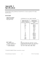
Page 47: ...Module Range1 Software Selectable 10 V 0 01 250 VDC or Vrms 0 02 250 V 0 05 200 V 0 1 100 V 0 2 50 V 0 5 20 V 1 10 V 2 5 V 5 2 V 10 1 V 20 500 mV 50 200 mV 100 100 mV 200 50 mV 500 20 mV 1 000 10 mV...

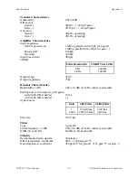
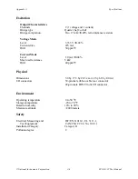
Page 48: ...width CMRR 50 or 60 Hz 4 Hz 160 dB 4 kHz 100 dB Output range 10 V Output impedance 75 Dynamic Characteristics Bandwidth 3 dB 4 Hz 10 dB or 4 kHz software selectable Settling time to full scale step al...

Page 49: ...m C Current Mode Level 1 0 mA 0 04 Max load resistance 5 k Drift 40 ppm C Physical Dimensions 3 0 by 17 3 by 20 3 cm 1 2 by 6 8 by 8 0 in I O connectors 50 pin male ribbon cable rear connector 48 pin...

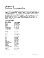
Page 50: ...central time In other countries contact the nearest branch office You may fax questions to us at any time Corporate Headquarters 512 795 8248 Branch Offices Phone Number Australia 03 9879 5166 Austria...

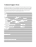
Page 51: ...iciently If you are using any National Instruments hardware or software products related to this problem include the configuration forms from their user manuals Include additional pages if necessary N...

Page 52: ...2 Revision Letter _____________________________________________________ Chassis Slot _____________________________________________________ Grounding Shielding and Reference Mode Selection Factory Sett...

Page 53: ...ogrammer manual Check all that apply National Instruments does not support your operating system or programming language You are an experienced register level programmer who is more comfortable writin...

Page 54: ...ptember 1999 Part Number 320516B 01 Please comment on the completeness clarity and organization of the manual If you find errors in the manual please record the page numbers and describe the errors Th...

Page 55: ...to less than negative of or minus ohms percent plus or minus positive of or plus 5 V signal 5 VDC Isolated Source signal A A amperes AC alternating current A D analog to digital ADIO Port A Digital I...

Page 56: ...og DAQD A Data Acquisition Board Data Address Line signal dB decibels DC direct current DIGGND Digital Ground signal DIN Deutsche Industrie Norme DOUT Data Out Number signal E EEPROM electrically eras...

Page 57: ...signal N NMR normal mode rejection NRSE nonreferenced single ended input O OUTREF Output Reference signal P ppm parts per million R R resistor RAM random access memory Rb bias resistor Rbias bias res...

Page 58: ...ace Clock signal T TEMP Temperature Sensor Reference signal TEMP Temperature Sensor Output signal V V volts Vcm common mode voltage VDC volts direct current VEX Voltage Excitation Channel signal VEX N...

Page 59: ...l 3 11 C cables custom cables 1 5 optional equipment table 1 4 calibration equipment requirements 5 1 to 5 2 excitation calibration 4 4 5 4 gain and offset calibration 5 2 to 5 3 overview 5 1 CH 0 15...

Page 60: ...ation 3 7 analog input channel signal connections 3 5 to 3 8 avoiding relay wear illustration 3 8 excitation channel signal connections 3 8 to 3 9 floating AC coupled signal connection referenced to c...

Page 61: ...rface 4 3 SCXIbus to SCXI 1122 rear signal connector to DAQ board pin equivalences table 3 13 signal descriptions 3 11 register level programming 1 4 registers Address Handler Register 4 3 Configurati...

Page 62: ...al 3 11 3 12 software programming choices LabVIEW applications software 1 2 LabWindows applications software 1 2 NI DAQ driver software 1 2 to 1 3 register level programming 1 4 specifications analog...

Reviews: