National Instruments SC Express PXIe-4331 User Manual Download Page 30

Chapter 2

Using the Module

©

 National Instruments Corporation

2-23

NI PXIe-4330/4331 User Manual

I/O Connector Signal Description

Table 2-2 describes the signals found on the I/O connector.

NI PXIe-4330/4331 Block Diagram

Figure 2-18 shows the analog input circuitry block diagram of the NI PXIe-4330/4331.The 
programmable excitation block provides the excitation voltage for the bridge or sensor. The 
voltage level is configurable on a per channel basis. This excitation voltage is sensed locally 
or remotely via the remote sense terminals (RS+ and RS–) and fed back to the ADC 
(Analog-to-Digital Converter) reference through a programmable gain amplifier. The gain 
applied when sensing the excitation voltage is automatically selected based on the selected 
excitation voltage level.
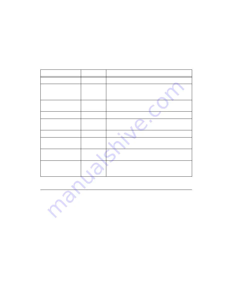
Table 2-2.  

I/O Connector Signal Descriptions

Signal Names

Direction

Description

AIGND

Analog Input Ground

AI<0..7>+, AI<0..7>–

Input

Analog Input Channels 0 to 7—AI+ and AI– are the 
positive and negative inputs of the differential analog 
input.

QTR/SC<0..7>

These pins provide the connection point for 
quarter-bridge completion and shunt calibration.

EX<0..7>+, EX<0..7>–

Output

Provides the differential bridge excitation voltage.

RS<0..7>+, RS<0..7>–

Input

Remote sense input. The remote sense pins sense the 
actual voltage applied to the bridge.

T<0..7>+

Input/Output

TEDS sensor digital communication lines.

T<0..7>–

Negative reference for TEDS communication. 
Internally connected to the module digital ground.

RSVD

These pins are reserved for communication with the 
accessory.

DGND

Digital ground—these pins supply the reference for 
module digital signals and are connected to the module 
digital ground.

Summary of Contents for SC Express PXIe-4331

Page 1: ...NI SC Express NI PXIe 4330 4331 User Manual NI PXIe 4330 4331 User Manual April 2010 373029A 01...

Page 2: ...Lebanon 961 0 1 33 28 28 Malaysia 1800 887710 Mexico 01 800 010 0793 Netherlands 31 0 348 433 466 New Zealand 0800 553 322 Norway 47 0 66 90 76 60 Poland 48 22 328 90 10 Portugal 351 210 311 210 Russ...

Page 3: ...mation retrieval system or translating in whole or in part without the prior written consent of National Instruments Corporation National Instruments respects the intellectual property of others and w...

Page 4: ...Half Bridge Type I 2 8 Half Bridge Type II 2 10 Full Bridge Type I 2 12 Full Bridge Type II 2 14 Full Bridge Type III 2 16 Force Pressure and Torque Sensor Configurations 2 18 Common Mode Voltage Con...

Page 5: ...Filters 3 3 Appendix A Offset Nulling Bridge Balancing Appendix B Technical Support and Professional Services Figures Figure 2 1 Basic Wheatstone Bridge Circuit Diagram 2 1 Figure 2 2 Connecting Remo...

Page 6: ...ridge Type III Circuit Diagram 2 17 Figure 2 17 Force Pressure and Torque Sensor Circuit Diagram 2 18 Figure 2 18 NI PXIe 4330 4331 Signal Conditioning Block Diagram 2 24 Figure 2 19 NI PXIe 4330 4331...

Page 7: ...rter half and full bridge Setting the DC voltage excitation between 0 625 V and 10 V Selecting 120 350 and 1 k quarter bridge completion resistors Programmable bridge offset null and shunt calibration...

Page 8: ...r to the NI SC Express 4330 4331 Installation Guide and Terminal Block Specifications for more signal connection information Wheatstone Bridges Many sensors including strain gages load cells pressure...

Page 9: ...lies it as a reference to its analog to digital converter ADC In this way variations in the excitation voltage are compensated for and the module returns data as a ratio of the bridge output voltage a...

Page 10: ...across the excitation lead wire resistance Rlead If you do not use remote sensing of the actual bridge voltage the resulting reduction in gain is given by the following equations for half bridge senso...

Page 11: ...strain by changing the resistance of an arm in the bridge by some known amount This is accomplished by shunting or connecting a large resistor of known value across one arm of the bridge creating a k...

Page 12: ...ion resistor located inside the NI PXIe 4330 4331 R3 must be equal to the nominal resistance of the active gage R4 RS Shunt calibration resistor located inside the NI PXIe 4330 4331 R4 Active element...

Page 13: ...nding configurations Figure 2 6 shows the quarter bridge type II circuit wiring diagram Figure 2 5 Quarter Bridge Type II Measuring Axial and Bending Strain A quarter bridge type II has the following...

Page 14: ...stor located inside the NI PXIe 4330 4331 R4 Active element measuring tensile strain RL Lead resistance GF Gage Factor specified by the gage manufacturer VCH Measured voltage of the bridge VEX Excitat...

Page 15: ...ns Figure 2 8 shows the half bridge type I circuit wiring diagram Figure 2 7 Half Bridge Type I Measuring Axial and Bending Strain A half bridge type I has the following characteristics Two active str...

Page 16: ...ring tensile strain RL Lead resistance GF Gage Factor specified by the gage manufacturer Poisson s ratio defined as the negative ratio of transverse strain to axial strain longitudinal strain Poisson...

Page 17: ...figuration Figure 2 10 shows the half bridge type II circuit wiring diagram Figure 2 9 Half Bridge Type II Rejecting Axial and Measuring Bending Strain A half bridge type II configuration has the foll...

Page 18: ...331 R4 Active element measuring tensile strain RL Lead resistance GF Gage Factor specified by the gage manufacturer VCH Measured voltage of the bridge VEX Excitation voltage provided by the NI PXIe 43...

Page 19: ...s the full bridge type I circuit wiring diagram Figure 2 11 Full Bridge Type I Rejecting Axial and Measuring Bending Strain A full bridge type I configuration has the following characteristics Four ac...

Page 20: ...libration resistor located inside the NI PXIe 4330 4331 RL Lead resistance GF Gage Factor specified by the gage manufacturer VCH Measured voltage of the bridge VEX Excitation voltage provided by the N...

Page 21: ...e 2 13 Full Bridge Type II Rejecting Axial and Measuring Bending Strain A full bridge type II configuration has the following characteristics Four active strain gage elements Two are mounted in the di...

Page 22: ...ed inside the NI PXIe 4330 4331 RL Lead resistance GF Gage Factor specified by the gage manufacturer Poisson s ratio defined as the negative ratio of transverse strain to axial strain longitudinal str...

Page 23: ...idge type III circuit wiring diagram Figure 2 15 Full Bridge Type III Measuring Axial and Rejecting Bending Strain A full bridge type III configuration has the following characteristics Four active st...

Page 24: ...r specified by the gage manufacturer Poisson s ratio defined as the negative ratio of transverse strain to axial strain longitudinal strain Poisson s ratio is a material property of the specimen you a...

Page 25: ...ensors typically use a full bridge configuration with a 350 nominal bridge resistance but other configurations and nominal bridge resistances can be used Figure 2 17 shows the force pressure torque se...

Page 26: ...are specified as pairs of corresponding physical and electrical values electrical1 physical1 and electrical2 physical2 These should be based on the calibration certificate of the sensor if one is avai...

Page 27: ...Considerations The NI PXIe 4330 4331 supports common mode voltages between 2 V The majority of full bridge sensors are balanced between the upper and lower arms of the bridge resulting in a common mo...

Page 28: ...reduce the excitation voltage to a level that results in a common mode voltage that is within range To find the maximum excitation voltage that meets this criterion solve the following equation setti...

Page 29: ...EX AI 2 25 QTR SC EX AI 24 QTR SC RS RS 23 AIGND EX AI 3 22 QTR SC EX AI 21 QTR SC RS RS 20 DGND T0 T1 No Channel 19 T3 T0 T1 18 T3 T2 T2 17 DGND T4 T5 16 T7 T4 T5 15 T7 T6 T6 14 AIGND EX AI 4 13 QTR...

Page 30: ...ected based on the selected excitation voltage level Table 2 2 I O Connector Signal Descriptions Signal Names Direction Description AIGND Analog Input Ground AI 0 7 AI 0 7 Input Analog Input Channels...

Page 31: ...an configure the NI PXIe 4330 4331 to select between internal 120 350 and 1 k quarter bridge completion resistors In addition you can enable programmable shunt calibration resistors individually or in...

Page 32: ...order to acquire data at the specified rate The DDS clock can be generated either using an onboard oscillator or using the 100 MHz backplane clock provided by PXI Express Running the DDS clock from t...

Page 33: ...nals with frequencies lower than fs 2 This maximum frequency is known as the Nyquist frequency The bandwidth from 0 Hz to the Nyquist frequency is the Nyquist bandwidth ADC The NI PXIe 4330 4331 ADCs...

Page 34: ...esented correctly while others contain aliased artifacts Lowpass filtering to eliminate components above the Nyquist frequency either before or during the digitization process can guarantee that the d...

Page 35: ...al filtering performed by the NI PXIe 4330 4331 produces a delay of many samples worth of time between when an event occurs on the input signal going into the NI PXIe 4330 4331 and when the data assoc...

Page 36: ...e maximum rate for the module Timing and Triggering This section contains information about timing and triggering theory of operation Sample Clock Timebase The ADCs require an oversample clock to driv...

Page 37: ...rigger samples The analog trigger on the NI PXIe 4330 4331 cannot be used as a start trigger This restriction is a result of the way the module compensates for the filter group delay When using an ana...

Page 38: ...ge triggering you add a window above or below the trigger level This triggering mode often is used to reduce false triggering due to noise or jitter in the signal For example if you add a hysteresis o...

Page 39: ...ses above 4 2 mV V as shown in Figure 2 22 Figure 2 22 Analog Edge Triggering with Hysteresis on Falling Slope Window Triggering A window trigger occurs when an analog signal either passes into enters...

Page 40: ...inate clock drift between modules in long duration operations You can synchronize the analog input operations on two or more NI PXIe 4330 4331 modules to extend the channel count for your measurements...

Page 41: ...slaves at DAQmx Trigger Advanced Synchronization Synchronization Type to Slave and that of the Master to Master Also query DAQmx Timing More Synchronization Pulse Synchronization Time on all modules...

Page 42: ...pop up menu To programmatically configure TEDS call the DAQmx Configure TEDS VI Accessory Auto Detection NI SC Express modules automatically detect compatible accessories or terminal blocks The RSVD p...

Page 43: ...ules in a PXI Express measurement or control system The PXI Express backplane is responsible for generating PXIe_SYNC100 independently to each peripheral slot in a PXI Express chassis For more informa...

Page 44: ...as a trigger signal for input operations An SC Express module is not a System timing controller An SC Express module can be used in the system timing slot of a PXI system but the system will not be a...

Page 45: ...s When the filter clock has sampled the signal high on N consecutive edges the low to high transition is propagated to the rest of the circuit The value of N depends on the filter setting Refer to Tab...

Page 46: ...e bridge while not under load and then use this measurement as the initial bridge voltage when scaling readings from the bridge This method is simple fast and requires no manual adjustments The disadv...

Page 47: ...you may renew to continue your benefits For information about other technical support options in your area visit ni com services or contact your local office at ni com contact Training and Certificati...

Page 48: ...PXIe 4330 4331 User Manual B 2 ni com this manual You also can visit the Worldwide Offices section of ni com niglobal to access the branch office Web sites which provide up to date contact information...

Reviews: