background image

Chapter 1

DAQ System Overview

©

 National Instruments Corporation

1-11

E Series User Manual

NI-DAQ\Examples\VBasic

 directory contains the examples not 

associated with Measurement Studio

NI-DAQmx examples for ANSI C are in the 

NI-DAQ\Examples\

DAQmx ANSI C Dev

 directory

Traditional NI-DAQ (Legacy) examples for ANSI C are in the 

NI-DAQ\Examples\VisualC

 directory

For additional examples, refer to 

zone.ni.com

.

I/O Connector Signal Descriptions

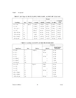
Table 1-4 describes the signals found on the I/O connectors. For a summary 
of the I/O signals by device family, refer to the specifications document for 
your device. Refer to Appendix A, 

Device-Specific Information

for the I/O 

pinout for your device.

Table 1-4.  

I/O Connector Signal Descriptions

Signal Name

Reference

Direction

Description

AI GND

AI Ground

—These pins are the reference point for 

single-ended AI measurements in RSE mode and the bias 
current return point for DIFF measurements. All three 
ground references—AI GND, AO GND, and D GND—are 
connected on the device.

AI <0..15>

AI GND

Input

AI Channels 0 through 15

—You can configure each 

channel pair, AI <

i

i

+8> (

i

 = 0..7), as either one differential 

input or two single-ended inputs.

AI <16..63>

AI GND

Input

AI Channels 16 through 63 
(NI PCI-6031E/6033E/6071E only)

—Each channel pair, 

AI <

i

i

 +8> (

i

 = 16..23, 32..39, 48..55), can be configured 

as either one differential input or two single-ended inputs.

AI SENSE

Input

AI Sense

—This pin is the reference node for AI <0..15> in 

NRSE mode.

AI SENSE 2

Input

AI Sense 2

—This pin is the reference node for 

AI <16..63> in NRSE mode.

AO 0

AO GND

Output

Analog Channel 0 Output

—This pin supplies the voltage 

output of AO channel 0.

AO 1

AO GND

Output

Analog Channel 1 Output

—This pin supplies the voltage 

output of AO channel 1.

AO GND

AO Ground

—The AO voltages are referenced to these 

pins. All three ground references—AI GND, AO GND, 
and D GND—are connected on the device.

Summary of Contents for PXI-6040E

Page 1: ...PXI 6040E ...

Page 2: ...DAQ E Series E Series User Manual E Series User Manual February 2007 370503K 01 ...

Page 3: ...0 Lebanon 961 0 1 33 28 28 Malaysia 1800 887710 Mexico 01 800 010 0793 Netherlands 31 0 348 433 466 New Zealand 0800 553 322 Norway 47 0 66 90 76 60 Poland 48 22 3390150 Portugal 351 210 311 210 Russia 7 495 783 6851 Singapore 1800 226 5886 Slovenia 386 3 425 42 00 South Africa 27 0 11 805 8197 Spain 34 91 640 0085 Sweden 46 0 8 587 895 00 Switzerland 41 56 2005151 Taiwan 886 02 2377 2222 Thailand...

Page 4: ...ng storing in an information retrieval system or translating in whole or in part without the prior written consent of National Instruments Corporation National Instruments respects the intellectual property of others and we ask our users to do the same NI software is protected by copyright and other intellectual property laws Where NI software may be used to reproduce software or other materials b...

Page 5: ...ent of Communications DOC Changes or modifications not expressly approved by NI could void the user s authority to operate the equipment under the FCC Rules Class A Federal Communications Commission This equipment has been tested and found to comply with the limits for a Class A digital device pursuant to part 15 of the FCC Rules These limits are designed to provide reasonable protection against h...

Page 6: ...ocumentation and Specifications xx Training Courses xx Technical Support on the Web xx Chapter 1 DAQ System Overview DAQ Hardware 1 2 DAQ STC 1 3 Calibration Circuitry 1 3 Internal or Self Calibration 1 4 External Calibration 1 4 Signal Conditioning 1 4 Sensors and Transducers 1 4 Signal Conditioning Options 1 5 SCXI 1 5 SCC 1 6 5B Series 1 6 Cables and Accessories 1 6 Using Accessories with Devic...

Page 7: ...nnels 2 11 Minimize Voltage Step between Adjacent Channels 2 12 Avoid Scanning Faster than Necessary 2 12 Example 1 2 12 Example 2 2 13 AI Data Acquisition Methods 2 13 Software Timed Acquisitions 2 13 Hardware Timed Acquisitions 2 13 Analog Input Triggering 2 14 AI Start Trigger Signal 2 15 Using a Digital Source 2 15 Using an Analog Source 2 15 Outputting the AI Start Trigger Signal 2 16 AI Refe...

Page 8: ...32 Using a Digital Source 2 33 Using an Analog Source 2 33 Outputting the AI Start Trigger Signal 2 33 AI Reference Trigger Signal 2 34 Using a Digital Source 2 35 Using an Analog Source 2 36 Outputting the AI Reference Trigger Signal 2 36 AI Pause Trigger Signal 2 36 Using a Digital Source 2 36 Using an Analog Source 2 37 AI Sample Clock Signal 2 37 Using an Internal Source 2 37 Using an External...

Page 9: ...og Source 3 6 Outputting the AO Start Trigger Signal 3 6 AO Pause Trigger Signal 3 7 Using a Digital Source 3 7 Using an Analog Source 3 7 Connecting Analog Output Signals 3 8 Waveform Generation Timing Signals 3 9 AO Start Trigger Signal 3 9 Using a Digital Source 3 9 Using an Analog Source 3 10 Outputting the AO Start Trigger Signal 3 10 AO Pause Trigger Signal 3 10 Using a Digital Source 3 10 U...

Page 10: ...tting Started with DIO Applications in Software 4 10 Chapter 5 Counters Counter Triggering 5 1 Start Trigger 5 1 Pause Trigger 5 2 Counter Timing Signals 5 2 Counter 0 Source Signal 5 3 Counter 0 Gate Signal 5 4 Counter 0 Internal Output Signal 5 5 CTR 0 OUT Pin 5 6 Counter 0 Up Down Signal 5 6 Counter 1 Source Signal 5 6 Counter 1 Gate Signal 5 7 Counter 1 Internal Output Signal 5 8 Counter 1 Up ...

Page 11: ...TE and DAQPnP 9 1 Using PXI with CompactPCI 9 1 Data Transfer Methods 9 2 Direct Memory Access DMA 9 2 Interrupt Request IRQ 9 2 Programmed I O 9 2 Changing Data Transfer Methods between DMA and IRQ 9 3 Chapter 10 Triggering Triggering with a Digital Source 10 1 Triggering with an Analog Source 10 2 PFI 0 AI START TRIG Pin 10 3 Analog Input Channel 10 3 Analog Trigger Actions 10 3 Analog Trigger T...

Page 12: ...Contents National Instruments Corporation xiii E Series User Manual Appendix B I O Connector Pinouts Appendix C Troubleshooting Appendix D Technical Support and Professional Services Glossary Index ...

Page 13: ... options to a final action The sequence File Page Setup Options directs you to pull down the File menu select the Page Setup item and select Options from the last dialog box This icon denotes a note which alerts you to important information This icon denotes a caution which advises you of precautions to take to avoid injury data loss or a system crash When this symbol is marked on the product refe...

Page 14: ...nstall your NI DAQmx supported DAQ device and how to confirm that your device is operating properly Select Start All Programs National Instruments NI DAQ DAQ Getting Started Guide The NI DAQ Readme lists which devices are supported by this version of NI DAQ Select Start All Programs National Instruments NI DAQ NI DAQ Readme The NI DAQmx Help contains general information about measurement concepts ...

Page 15: ...ed by this version of NI DAQmx Base Select Start All Programs National Instruments NI DAQmx Base DAQmx Base Readme The NI DAQmx Base VI Reference Help contains VI reference and general information about measurement concepts In LabVIEW select Help NI DAQmx Base VI Reference Help The NI DAQmx Base C Reference Help contains C reference and general information about measurement concepts Select Start A...

Page 16: ...tep instructions about creating a measurement task using the DAQ Assistant In LabWindows CVI select Help Contents then select Using LabWindows CVI Data Acquisition The NI DAQmx Library book of the LabWindows CVI Help contains API overviews and function reference for NI DAQmx Select Library Reference NI DAQmx Library in the LabWindows CVI Help Measurement Studio If you program your NI DAQmx support...

Page 17: ... Traditional NI DAQ Legacy Function Reference Help and NI DAQmx C Reference Help describe the C functions and attributes Select Start All Programs National Instruments NI DAQ and the document title for the NI DAQ API you are using NET Languages without NI Application Software With the Microsoft NET Framework version 1 1 or later you can use NI DAQmx to create applications using Visual C and Visual...

Page 18: ...he Device Document Browser device documents are accessible from Start All Programs National Instruments NI DAQ Browse Device Documentation Training Courses If you need more help getting started developing an application with NI products NI offers training courses To enroll in a course or obtain a detailed course outline refer to ni com training Technical Support on the Web For additional support r...

Page 19: ...shows a typical DAQ system setup which includes transducers signal conditioning cables that connect the various devices to the accessories the E Series device and the programming software Refer to the Using Accessories with Devices section for a list of devices and their compatible accessories ...

Page 20: ...Hardware DAQ hardware digitizes signals performs D A conversions to generate analog output signals and measures and controls digital I O signals 1 Sensors and Transducers 2 Terminal Block Accessory 3 SCXI Module 4 SCXI Chassis 5 Cable Assembly 6 DAQ Device 7 Personal Computer V HV mV 1 2 3 4 5 6 7 ...

Page 21: ...l output Calibration Circuitry Calibration is the process of making adjustments to a measurement device to reduce errors associated with measurements Without calibration the measurement results of your device will drift over time and temperature Calibration adjusts for these changes to improve measurement accuracy and ensure that your product meets its required specifications DAQ devices have high...

Page 22: ...e NI 6013 NI 6014 NI 6015 and NI 6016 using NI DAQmx refer to the E S M B Series Calibration Procedure for NI DAQmx For a detailed calibration procedure for B E Series devices using Traditional NI DAQ Legacy refer to the E Series Calibration Procedure These documents can be found by selecting Manual Calibration Procedures at ni com calibration Signal Conditioning Many sensors and transducers requi...

Page 23: ...plication software refer to Common Sensors in the NI DAQmx Help which you can access from Start All Programs National Instruments NI DAQ NI DAQmx Help or the LabVIEW 8 x Help Signal Conditioning Options SCXI SCXI is a front end signal conditioning and switching system for various measurement devices including E Series devices An SCXI system consists of a rugged chassis that houses shielded signal ...

Page 24: ...le portable Integrates well with other laptop computer measurement technologies High bandwidth Acquire signals at rates up to 1 25 MHz Connectivity Incorporates panelette technology to offer custom connectivity to thermocouple BNC LEMO B Series and MIL Spec connectors 5B Series 5B is a front end signal conditioning system for plug in data acquisition devices A 5B system consists of eight or 16 sin...

Page 25: ...onnect an E Series device and an accessory 1 Select an E Series device 2 Using Table 1 1 or Table 1 2 as a guide determine which accessories are appropriate for that device Select an accessory Table 1 3 provides descriptions for E Series device accessories 3 Using Table 1 1 or Table 1 2 as a guide determine which cable is required to connect your selected device and accessory Table 1 1 68 Pin and ...

Page 26: ...ese accessories are used with the second 68 pin connector SH100100 shielded 100 pin E Series with 16 AI channels and 32 DIO lines NI PCI 6025E SH1006868 shielded splits into two 68 pin connectors these accessories are used with the first 68 pin connector SH1006868 shielded splits into two 68 pin connectors these accessories are used with the second 68 pin connector SH1006868 shielded splits into t...

Page 27: ...nnectors and a back shell kit for making custom 68 pin cables are available from NI For more information about the 68 and 100 pin BNC 2111 BNC accessory for 68 or 100 pin E Series devices BNC 2115 BNC accessory for extended I O on 100 pin E Series devices BNC 2120 BNC accessory with function generator for 68 pin E Series devices BNC 2090 Rack mountable BNC accessory for 68 pin E Series devices CA ...

Page 28: ... Getting Started Guide for more information about the two drivers Traditional NI DAQ Legacy and NI DAQmx each include a collection of programming examples to help you get started developing an application You can modify example code and save it in an application You can use examples to develop a new application or add example code to an existing application To locate LabVIEW and LabWindows CVI exa...

Page 29: ...le ended AI measurements in RSE mode and the bias current return point for DIFF measurements All three ground references AI GND AO GND and D GND are connected on the device AI 0 15 AI GND Input AI Channels 0 through 15 You can configure each channel pair AI i i 8 i 0 7 as either one differential input or two single ended inputs AI 16 63 AI GND Input AI Channels 16 through 63 NI PCI 6031E 6033E 607...

Page 30: ...peripheral interface P3 7 is the MSB P3 0 is the LSB 5 V D GND Output 5 V Power Source These pins provide 5 V power AI HOLD COMP D GND Output AI Hold Complete Event Signal When enabled this signal pulses once for each A D conversion in sampling mode The low to high edge indicates when the input signal can be removed from the input or switched to another signal EXT STROBE D GND Output External Stro...

Page 31: ...l As an output this pin is the Ctr1Gate signal This signal reflects the actual gate signal connected to the general purpose Counter 1 CTR 1 OUT D GND Input CTR 1 OUT As an input this pin can be used to route signals directly to the RTSI bus Output Counter 1 Output Signal As an output this pin emits the Ctr1InternalOutput signal PFI 5 AO SAMP CLK D GND Input PFI 5 As an input this pin is a PFI Outp...

Page 32: ...put PFI 9 As an input this pin is a PFI Output Counter 0 Gate Signal As an output this pin is the Ctr0Gate signal This signal reflects the actual gate signal connected to the general purpose Counter 0 CTR 1 OUT D GND Input Counter 1 Output Signal As an input this pin can be used to route signals directly to the RTSI bus Output As an output this pin emits the Ctr0InternalOutput signal FREQ OUT USER...

Page 33: ...P0 DIOA DIOB DIOC P0 P1 P2 EXTREF AO EXT REF or EXT REF EXT_STROBE EXT STROBE EXT_TRIG EXT TRIG EXT_CONV EXT CONV FREQ_OUT FREQ OUT or F OUT GPCTR0_GATE CTR 0 GATE GPCTR0_OUT CTR 0 OUT GPCTR0_SOURCE CTR 0 SOURCE or CTR 0 SRC GPCTR1_GATE CTR 1 GATE GPCTR1_OUT CTR 1 OUT GPCTR1_SOURCE CTR 1 SOURCE or CTR 1 SRC PA PB PC P0 P1 P2 PFI PFI PFI_ PFI PCLK PFI Table 1 5 Terminal Name Equivalents Continued T...

Page 34: ...o find your device power rating refer to the specifications document for your device Caution Never connect these 5 V power pins to analog or digital ground or to any other voltage source on the E Series device or any other device Doing so can damage the device and the computer NI is not liable for damage resulting from such a connection REQ PFI SCANCLK AI HOLD COMP or AI HOLD SISOURCE AI Sample Cl...

Page 35: ...ed determine how you connect these AI signals to the E Series devices This chapter provides an overview of the different types of signal sources and AI configuration modes Analog Input Circuitry Mux Each E Series device has one analog to digital converter ADC The multiplexer mux routes one AI channel at a time to the ADC through the NI PGIA The mux also gives you the ability to use three different...

Page 36: ... digital number AI FIFO A large first in first out FIFO buffer holds data during A D conversions to ensure that no data is lost E Series devices can handle multiple A D conversion operations with DMA interrupts or programmed I O Analog Trigger Refer to the Analog Input Triggering section for information about the trigger circuitry of E Series devices AI Timing Signals Refer to the Analog Input Tim...

Page 37: ...ut range that matches the expected input range of your signal A large input range can accommodate a large signal variation but reduces the voltage resolution Choosing a smaller input range improves the voltage resolution but may result in the input signal going out of range For more information about programming these settings refer to the NI DAQmx Help or the LabVIEW 8 x Help Tables 2 1 2 2 and 2...

Page 38: ...le 2 2 Input Ranges for NI 6011E and NI 6030E 6031E 6032E 6033E Input Range Gain Polarity Precision NI 6011E NI 6030E 6030E 6032E 6033E 0 to 10 V 0 to 5 V 0 to 2 V 0 to 1 V 0 to 500 mV 0 to 200 mV 0 to 100 mV 1 2 5 10 20 50 100 Unipolar 153 µV 76 3 µV 15 3 µV 1 53 µV 153 µV 76 3 µV 30 5 µV 15 3 µV 7 63 µV 3 05 µV 1 53 mV 10 to 10 V 5 to 5 V 2 to 2 V 1 to 1 V 500 to 500 mV 200 to 200 mV 100 to 100 ...

Page 39: ...ion for more information about using these input configurations Table 2 3 Input Ranges for NI 6023E 6024E 6025E and NI 6034E 6035E 6036E Input Range Gain Resolution NI 6023E 6024E 6025E NI 6034E 6035E 6036E 10 to 10 V 0 5 4 88 mV 305 µV 5 to 5 V 1 2 44 mV 153 µV 500 to 500 mV 10 244 µV 15 3 µV 50 to 50 mV 100 24 4 µV 1 53 µV Table 2 4 Analog Input Terminal Configuration AI Terminal Configuration D...

Page 40: ...IA in a different way The PGIA applies gain and common mode voltage rejection and presents high input impedance to the AI signals connected to the device Signals are routed to the positive and negative inputs of the PGIA through input multiplexers on the device The PGIA converts two input signals to a new signal by taking the difference between the two input signals and multiplying the difference ...

Page 41: ...amage resulting from such signal connections The maximum input voltage ratings are listed in the specifications document for each E Series family NI 6031E NI 6033E and NI 6071E Only For these extended AI devices the AI signals are AI 0 63 AI SENSE AI SENSE 2 and AI GND In single ended mode signals connected to AI 0 63 are routed to the positive input of the PGIA In differential mode signals connec...

Page 42: ... reading This process removes the effects of quantization and reduces measurement noise resulting in improved resolution For high speed applications not involving averaging or spectral analysis you may want to disable dithering to reduce noise The software enables and disables the dithering circuitry Figure 2 3 illustrates the effect of dithering on signal acquisition Graph A shows a small 4 LSB s...

Page 43: ...AI channel the device configures the NI PGIA with the input range of the new channel The NI PGIA then amplifies the input signal with the gain and polarity for the new input range Settling time refers to the time it takes the NI PGIA to amplify the input signal to the desired accuracy before it is sampled by the ADC The specification document for your DAQ device shows its settling time 6 0 4 0 2 0...

Page 44: ...dances of 1 kΩ The settling time specifications for your device assume a 1 kΩ source Large source impedances increase the settling time of the PGIA and so decrease the accuracy at fast scanning rates Settling times increase when scanning high impedance signals due to a phenomenon called charge injection Multiplexers contain switches usually made of switched capacitors When one of the channels for ...

Page 45: ...1 mV The approximately 4 V step from 4 V to 1 mV is 4 000 of the new full scale range For a 12 bit device to settle within 0 012 120 ppm or 1 2 LSB of the 100 mV full scale range on channel 1 the input circuitry must settle to within 0 0003 3 ppm or 1 80 LSB of the 4 V step Some devices can take as long as 100 µs for the circuitry to settle this much To avoid this effect you should arrange your ch...

Page 46: ...ry between 4 V and 0 V Scanning channels in the order 0 2 4 1 3 5 will produce more accurate results than scanning channels in the order 0 1 2 3 4 5 Avoid Scanning Faster than Necessary Designing your system to scan at slower speeds gives the PGIA more time to settle to a more accurate level Consider the following examples Example 1 Averaging many AI samples can increase the accuracy of the readin...

Page 47: ...ons hardware timed acquisitions can be buffered or non buffered Software Timed Acquisitions With a software timed acquisition software controls the rate of the acquisition Software sends a separate command to the hardware to initiate each ADC conversion In NI DAQmx software timed acquisitions are referred to as having On Demand timing software timed acquisitions are also referred to as immediate o...

Page 48: ...ta samples and stopping a continuous acquisition continues until you stop the operation A continuous acquisition is also referred to as double buffered or circular buffered acquisition If data cannot be transferred across the bus fast enough the data in the FIFO will be overwritten and an error will be generated With continuous operations if the user program does not read data out of the PC buffer...

Page 49: ...urce specify a source and an edge The source can be an external signal connected to any PFI or RTSI 0 6 pin The source can also be one of several internal signals on your DAQ device Refer to Device Routing in MAX in the NI DAQmx Help or the LabVIEW 8 x Help for more information Also specify whether the measurement acquisition begins on the rising edge or falling edge of the ai StartTrigger signal ...

Page 50: ...the AI Reference Trigger Signal section for a complete description of the use of ai StartTrigger and ai ReferenceTrigger in a pretrigger DAQ operation AI Reference Trigger Signal You can use the AI Reference Trigger ai ReferenceTrigger signal to stop a measurement acquisition In Traditional NI DAQ Legacy a reference trigger is referred to as a stop trigger To use a reference trigger specify a buff...

Page 51: ...itations before the DAQ device discards it Refer to the KnowledgeBase document Can a Pretriggered Acquisition be Continuous for more information When the reference trigger occurs the DAQ device continues to write samples to the buffer until the buffer contains the desired number of posttrigger samples Figure 2 6 shows the final buffer Figure 2 6 Reference Trigger Final Buffer Pre Trigger Samples R...

Page 52: ...igger signal Figure 2 7 shows the timing requirements of the ai ReferenceTrigger source Figure 2 7 ai ReferenceTrigger Source Timing Requirements Using an Analog Source When you use an analog trigger source the acquisition stops on the first rising edge of the Analog Comparison Event signal Refer to the Triggering with an Analog Source section of Chapter 10 Triggering for more information on analo...

Page 53: ...urce can be an external signal connected to any PFI or RTSI 0 6 pin The source can also be one of several other internal signals on your DAQ device Refer to Device Routing in MAX in the NI DAQmx Help or the LabVIEW 8 x Help for more information Also specify whether the measurement sample is paused when ai PauseTrigger is at a logic high or low level Using an Analog Source When you use an analog tr...

Page 54: ... following sections discuss the types of signal sources specify the use of single ended and DIFF measurements and provide recommendations for measuring both floating and ground referenced signal sources Table 2 6 summarizes the recommended input configuration for both types of signal sources ...

Page 55: ...ect To Building Ground Ground Referenced Signal Sources Examples Ungrounded thermocouples Signal conditioning with isolated outputs Battery devices Examples Plug in instruments with non isolated outputs Differential DIFF Single Ended Ground Referenced RSE Single Ended Non Referenced NRSE Vs AI AI GND Rext AI Vs AI AI AI GND Vs AI AI GND V1 AI Vg AI GND Ground loop losses Vg are added to measured s...

Page 56: ...int with respect to the device assuming that the computer is plugged into the same power system as the source Non isolated outputs of instruments and devices that plug into the building power system fall into this category The difference in ground potential between two instruments connected to the same building power system is typically between 1 and 100 mV but the difference can be much higher if...

Page 57: ...h noisy environments DIFF signal connections reduce noise pickup and increase common mode noise rejection DIFF signal connections also allow input signals to float within the common mode limits of the PGIA Differential Connections for Ground Referenced Signal Sources Figure 2 9 shows how to connect a ground referenced signal source to a channel on the device configured in DIFF mode Figure 2 9 Diff...

Page 58: ...al source and the device In addition with DIFF input connections the PGIA can reject common mode noise pickup in the leads connecting the signal sources to the device The PGIA can reject common mode signals as long as AI and AI input signals are both within 11 V of AI GND Differential Connections for Non Referenced or Floating Signal Sources Figure 2 10 shows how to connect a floating signal sourc...

Page 59: ...ce impedance The resistor puts the signal path nearly in balance so that about the same amount of noise couples onto both connections yielding better rejection of electrostatically coupled noise This configuration does not load down the source other than the very high input impedance of the PGIA You can fully balance the signal path by connecting another resistor of the same value between the posi...

Page 60: ...ase the device provides the reference ground point for the external signal NRSE input mode is used for ground referenced signal sources in this case the external signal supplies its own reference ground point and the device should not supply one Refer to the DAQ Assistant Help for more information about the DAQ Assistant In the single ended modes more electrostatic and magnetic noise couples into ...

Page 61: ...e input of the PGIA and connect the signal local ground reference to the negative input of the PGIA The ground point of the signal therefore connects to the AI SENSE pin as shown in Figure 2 12 Any potential difference between the device ground and the signal ground appears as a common mode signal at both the positive and negative inputs of the PGIA and this difference is rejected by the amplifier...

Page 62: ...ject common mode noise Use individually shielded twisted pair wires to connect AI signals to the device With this type of wire the signals attached to the positive and negative input channels are twisted together and then covered with a shield You then connect this shield only at one point to the signal source ground This kind of connection is required for signals traveling through areas with larg...

Page 63: ...trol of the AI Config VI This input has a one to one correspondence with the channels control of the VI You must list all channels either individually or in groups of channels with the same input configuration For example if you want AI 0 to be differential and AI 1 and AI 2 to be RSE Figure 2 13 demonstrates how to program this configuration in LabVIEW Figure 2 13 AI Config VI To enable multi mod...

Page 64: ...ing engine Figure 2 15 Analog Input Timing Engine Clock Routing and Timing Options E Series devices use the ai SampleClock and ai ConvertClock signals to perform interval sampling As Figure 2 16 shows ai SampleClock controls the sample period which is determined by the following equation 1 sample period sample rate 200 RTSI 7 20 MHz Timebase Onboard Clock PFI 0 9 RTSI 0 6 Onboard Clock ai SampleCl...

Page 65: ...or example if an E Series device has a sampling rate of 200 kS s this sampling rate is aggregate one channel at 200 kS s or two channels at 100 kS s per channel illustrates the relationship An acquisition with posttrigger data allows you to view data that is acquired after a trigger event is received A typical posttrigger DAQ sequence is shown in Figure 2 17 The sample counter is loaded with the s...

Page 66: ...Acquisition If an ai ReferenceTrigger pulse occurs before the specified number of pretrigger samples are acquired the trigger pulse is ignored Otherwise when the ai ReferenceTrigger pulse occurs the sample counter value decrements until the specified number of posttrigger samples have been acquired Refer to the Analog Input Triggering section for more information about start and reference triggers...

Page 67: ...e rising edge or falling edge of the ai StartTrigger signal Figure 2 19 shows the timing requirements of the ai StartTrigger source Figure 2 19 ai StartTrigger Timing Requirements Using an Analog Source When you use an analog trigger source the acquisition begins on the first rising edge of the Analog Comparison Event signal Refer to Chapter 10 Triggering for more information on analog triggering ...

Page 68: ...uisition In Traditional NI DAQ Legacy a reference trigger is referred to as a stop trigger To use a reference trigger specify a buffer of finite size and a number of pretrigger samples samples that occur before the reference trigger The desired number of posttrigger samples samples that occur after the reference trigger is the buffer size minus the number of pretrigger samples Once the acquisition...

Page 69: ... can be an external signal connected to any PFI or RTSI 0 6 pin The source can also be one of several internal signals on your DAQ device Refer to Device Routing in MAX in the NI DAQmx Help or the LabVIEW 8 x Help for more information Also specify whether the measurement acquisition stops on the rising edge or falling edge of the ai ReferenceTrigger signal Figure 2 22 shows the timing requirements...

Page 70: ...of the PFI 1 AI REF TRIG pin configured as an output Figure 2 23 PFI 1 AI REF TRIG Timing Behavior The PFI 1 AI REF TRIG pin is configured as an input by default AI Pause Trigger Signal You can use the AI Pause Trigger ai PauseTrigger signal to pause and resume a measurement acquisition This signal is not available as an output Using a Digital Source To use ai PauseTrigger specify a source and a p...

Page 71: ...list once for every ai SampleClock A measurement acquisition consists of one or more samples The source of the ai SampleClock signal can be internal or external You specify whether the measurement sample begins on the rising edge or falling edge of the ai SampleClock signal Using an Internal Source By default ai SampleClock is created internally by dividing down the ai SampleClockTimebase Refer to...

Page 72: ...vior your DAQ device briefly pulses the PFI 7 AI SAMP CLK pin once for every occurrence of ai SampleClock With level behavior your DAQ device drives PFI 7 AI SAMP CLK high during the entire sample The device drives the pin high in response to the ai StartTrigger signal The device drives the pin low in response to the last ai ConvertClock of the sample Figures 2 25 and 2 26 show the timing of pulse...

Page 73: ...also specify a configurable delay from the ai StartTrigger to the first ai SampleClock pulse By default this delay is two ticks of the ai SampleClockTimebase signal When using an externally generated ai SampleClock in NI DAQmx you must ensure the clock signal is matched with respect to the timing requirements of the ai ConvertClock signal Failure to do so may result in ai SampleClock pulses that a...

Page 74: ... Onboard Clock source for the ai SampleClock You can configure the polarity selection for ai SampleClockTimebase as either rising or falling edge The maximum allowed frequency is 20 MHz with a minimum pulse width of 23 ns high or low There is no minimum frequency limitation The 20MHzTimebase or the 100kHzTimebase generates ai SampleClockTimebase unless you select some external source Figure 2 28 s...

Page 75: ...stest conversion rate possible for the device with 10 µs of delay added between each conversion to allow the channel to some time settle Caution Setting the conversion rate higher than the maximum rate specified for your device will result in errors Using an Internal Source One of the following internal signals can drive ai ConvertClock CTR 0 OUT the output of Counter 0 AI Convert Clock Timebase d...

Page 76: ...putting the AI Convert Clock Signal You can configure the PFI 2 AI CONV CLK pin to output the ai ConvertClock signal The output pin reflects the ai ConvertClock signal regardless of what signal you specify as its source Figure 2 30 shows the timing of behavior of the PFI 2 AI CONV CLK pin configured as an output Figure 2 30 PFI 2 AI CONV CLK Timing Behavior The PFI 2 AI CONV CLK pin is configured ...

Page 77: ...unless the proper timing requirements are met For example the device ignores both the ai SampleClock and ai ConvertClock until it receives a valid ai StartTrigger signal Once the device recognizes an ai SampleClock pulse it ignores subsequent ai SampleClock pulses until it receives the correct number of ai ConvertClock pulses Similarly the device ignores all ai ConvertClock pulses until it recogni...

Page 78: ...ast for Convert Clock Sample Clock pulses are gated off ai ConvertClock ai SampleClock 1 2 3 Convert Clock too fast for Sample Clock Convert Clock pulses are gated off ai ConvertClock ai SampleClock 1 2 3 Improperly matched Sample Clock and Convert Clock Leads to aperiodic sampling ai ConvertClock ai SampleClock 1 2 3 Properly matched Sample Clock and Convert Clock ...

Page 79: ...og input analog output and counter subsystems It is available as an output on the I O connector but you must use one or more counters to do so The maximum allowed frequency for the MasterTimebase is 20 MHz with a minimum pulse width of 23 ns high or low There is no minimum frequency limitation The two possible sources for the MasterTimebase signal are the internal 20MHzTimebase signal or an extern...

Page 80: ...Figure 2 34 ai HoldCompleteEvent Timing External Strobe Signal External Strobe is an output only signal on the EXT STROBE pin that generates either a single pulse or a sequence of eight pulses in the hardware strobe mode An external device can use this signal to latch signals or to trigger events In the single pulse mode software controls the level of External Strobe A 10 ms and a 1 2 µs clock are...

Page 81: ... applications Single Point Analog Input Finite Analog Input Continuous Analog Input You can perform these applications through DMA interrupt or programmed I O data transfer mechanisms Some of the applications also use start reference and pause triggers For more information about programming analog input applications and triggers in software refer to the NI DAQmx Help or the LabVIEW 8 x Help ...

Page 82: ...rm generation Refer to Appendix A Device Specific Information for specific information about the capabilities of your device Analog Output Circuitry DACs Digital to analog converters DACs convert digital codes to analog voltages DAC FIFO The DAC FIFO enables analog output waveform generation It is a first in first out FIFO memory buffer between the computer and the DACs that allows you to download...

Page 83: ...vices such as the NI 6013 6014 and NI 6015 6016 are bipolar only with an internal reference Refer to the specifications document for your device for more information about range setting options Reference Selection NI 6020E NI PXI 6040E NI 6052E NI 6062E NI 6070E 6071E and PCI MIO 16E 4 Devices Only You can connect each DAC to the device internal reference of 10 V or to the external reference signa...

Page 84: ... values written to the AO channel range must be positive Reglitch Selection NI 6052E and NI 6070E 6071E Devices Only In normal operation a DAC output glitches whenever it is updated with a new value The glitch energy differs from code to code and appears as distortion in the frequency spectrum Each analog output contains a reglitch circuit that generates uniform glitch energy at every code rather ...

Page 85: ... signal controls the rate of the generation This signal can be generated internally on your device or provided externally Hardware timed generations have several advantages over software timed generations The time between samples can be much shorter The timing between samples can be deterministic Hardware timed generations can use hardware triggering Hardware timed operations can be buffered or no...

Page 86: ...om there Once the data is downloaded new data cannot be written to the FIFO To use FIFO regeneration the entire buffer must fit within the FIFO size The advantage of using FIFO regeneration is that it does not require communication with the main host memory once the operation is started thereby preventing any problems that may occur due to excessive bus traffic With non regeneration old data will ...

Page 87: ...Qmx Help or the LabVIEW 8 x Help for more information Figure 3 2 shows the timing requirements of the ao StartTrigger digital source Figure 3 2 ao StartTrigger Digital Source Timing Requirements Using an Analog Source When you use an analog trigger source the waveform generation begins on the first rising edge of the Analog Comparison Event signal Refer to Chapter 10 Triggering for more informatio...

Page 88: ...use does not take effect until the beginning of the next sample This signal is not available as an output Using a Digital Source To use ao PauseTrigger specify a source and a polarity The source can be an external signal connected to any PFI or RTSI 0 6 pin The source can also be one of several other internal signals on your DAQ device Refer to Device Routing in MAX in the NI DAQmx Help or the Lab...

Page 89: ...annel 1 AO GND is the ground reference signal for both AO channels and the external reference signal Figure 3 4 shows how to make AO connections to the device Figure 3 4 Analog Output Connections Note Not all E Series devices use the external reference signal Refer to the specifications document for your device Load Load V OUT V OUT AO GND AO 1 Analog Output Channels E Series Device AO 0 Channel 1...

Page 90: ...oftware command Using a Digital Source To use ao StartTrigger specify a source and an edge The source can be an external signal connected to any PFI or RTSI 0 6 pin The source can also be one of several internal signal on your DAQ device Refer to Device Routing in MAX in the NI DAQmx Help or the LabVIEW 8 x Help for more information Figure 3 6 shows the timing requirements of the ao StartTrigger d...

Page 91: ...ming Behavior The PFI 6 AO START TRIG pin is configured as an input by default AO Pause Trigger Signal You can use the AO Pause trigger signal ao PauseTrigger to mask off samples in a DAQ sequence That is when ao PauseTrigger is active no samples occur The ao PauseTrigger does not stop a sample that is in progress The pause does not take effect until the beginning of the next sample This signal is...

Page 92: ...l or external You can specify whether the DAC update begins on the rising edge or falling edge of the ao SampleClock signal Using an Internal Source By default ao SampleClock is created internally by dividing down the ao SampleClockTimebase Several other internal signals can be routed to the sample clock Refer to Device Routing in MAX in the NI DAQmx Help or the LabVIEW 8 x Help for more informati...

Page 93: ...5 AO SAMP CLK Timing Behavior The PFI 5 AO SAMP CLK is configured as an input by default Other Timing Requirements A counter on your device internally generates ao SampleClock unless you select some external source The ao StartTrigger signal starts this counter It is stopped automatically by hardware once a finite acquisition completes or manually through software When using an internally generate...

Page 94: ...o SampleClockTimebase is divided down to provide the Onboard Clock source for the ao SampleClock You specify whether the samples begin on the rising or falling edge of ao SampleClockTimebase You might use the ao SampleClockTimebase signal if you want to use an external sample clock signal but need to divide the signal down If you want to use an external sample clock signal but do not need to divid...

Page 95: ... on the board are derived It controls the timing for the analog input analog output and counter subsystems It is available as an output on the I O connector but you must use one or more counters to do so The maximum allowed frequency for the MasterTimebase is 20 MHz with a minimum pulse width of 23 ns high or low There is no minimum frequency limitation The two possible sources for the MasterTimeb...

Page 96: ...e following analog output applications Single Point Generation Finite Generation Continuous Generation Waveform Generation You can perform these generations through DMA interrupt or programmed I O data transfer mechanisms Some of the applications also use start triggers and pause triggers Note For more information about programming analog output applications and triggers in software refer to the N...

Page 97: ...ircuitry of the E Series device Figure 4 1 DIO Circuitry Block Diagram E Series devices contain eight lines of DIO P0 0 7 for general purpose use You can individually configure each line with software for either input Data Out Output Enable Data In Protection Data Out Output Enable Data In Protection ...

Page 98: ...ode 0 strobed I O mode 1 and bidirectional I O mode 2 In modes 1 and 2 the three ports are divided into two groups group A and group B Each group has eight data bits plus control and status bits from Port 3 P3 Modes 1 and 2 use handshaking signals from the computer to synchronize data transfers NI DAQmx does not currently support mode 2 The Example Finder contains examples for programming the 82C5...

Page 99: ...m value on the line is 0 4 VDC The DIO lines provide a maximum of 2 5 mA at 3 7 V in the high state Using the largest possible resistor ensures that you do not use more current than necessary to perform the pull down task Ensure the value of the resistor is not so large that leakage current from the DIO line along with the current from the 100 kΩ pull up resistor drives the Table 4 1 Configuration...

Page 100: ...here V 0 4 V Voltage across RL I 46 µA 4 6 V across the 100 kΩ pull up resistor 10 µA 10 µA maximum leakage current Therefore RL 7 1 kΩ 0 4 V 56 µA This resistor value 7 1 kΩ provides a maximum of 0 4 V on the DIO line at power on You can substitute smaller resistor values to lower the voltage or to provide a margin for Vcc variations and other factors Timing Specifications NI 6016 and NI 6025E De...

Page 101: ...vice indicating that it has received the data from your DIO device OBF Output Output buffer full A low signal on this handshaking line indicates that data has been written to the port INTR Output Interrupt request This signal becomes high when the 82C55A requests service during a data transfer You must set the appropriate interrupt enable bits to generate this signal RD Internal Read This signal i...

Page 102: ...transfer in mode 1 Figure 4 3 Input Transfer in Mode 1 Timing Specifications Table 4 3 Input Transfer in Mode 1 Timing Specifications Name Description Minimum ns Maximum ns T1 STB Pulse Width 100 T2 STB 0 to IBF 1 150 T3 Data before STB 1 20 T4 STB 1 to INTR 1 150 T5 Data after STB 1 50 T6 RD 0 to INTR 0 200 T7 STB Pulse Width 150 T1 T2 T4 T7 T6 T3 T5 STB IBF INTR RD DATA ...

Page 103: ...n output transfer in mode 1 Figure 4 4 Output Transfer in Mode 1 Timing Specifications Table 4 4 Output Transfer in Mode 1 Timing Specifications Name Description Minimum ns Maximum ns T1 WR 0 to INTR 0 250 T2 WR 1 to Output 200 T3 WR 1 to OBF 0 150 T4 ACK 0 to OBF 1 150 T5 ACK Pulse Width 100 T6 ACK 1 to INTR 1 150 WR OBF INTR ACK DATA T1 T2 T3 T4 T5 T6 WR OBF INTR ACK DATA T1 T2 T3 T4 T5 T6 ...

Page 104: ...ional Transfer Timing Specifications Table 4 5 Bidirectional Transfer Timing Specification Name Description Minimum ns Maximum ns T1 WR 1 to OBF 0 150 T2 Data before STB 1 20 T3 STB Pulse Width 100 T4 STB 0 to IBF 1 150 T5 Data after STB 1 50 T6 ACK 0 to OBF 1 150 T7 ACK Pulse Width 100 T8 ACK 0 to Output 150 T9 ACK 1 to Output Float 20 250 T10 RD 1 to IBF 0 150 T1 T6 T7 T3 T4 T10 T2 T5 T8 T9 WR O...

Page 105: ...resistor This pull up resistor sets the P0 0 pin to a logic high when the output is in a high impedance state Caution If you enable a PFI line for output do not connect any external signal source to it Doing so could damage the device the computer and the connected equipment Connecting Digital I O Signals All devices have DIO signals P0 0 7 and D GND P0 0 7 are the eight digital lines making up th...

Page 106: ...and the computer NI is not liable for any damage resulting from such signal connections Getting Started with DIO Applications in Software You can use the E Series device in the following digital I O applications Static Digital Input Static Digital Output NI 6016 and NI 6025E Devices Only Handshaking Note For more information about programming digital I O applications and triggers in software refer...

Page 107: ...r can directly initiate these actions An analog trigger can indirectly initiate these actions by routing the Analog Comparison Event from a triggered analog input or output task to the counter as a digital trigger Start Trigger A start trigger begins a finite or continuous pulse generation Once a continuous generation is initiated the pulses continue to generate until you stop the operation in sof...

Page 108: ...ising edge of the source signal This timing diagram assumes that the counters are programmed to count rising edges The same timing diagram but with the source signal inverted and referenced to the falling edge of the source signal applies when you program the counter to count falling edges The gate input timing parameters are referenced to the signal at the source input or to one of the internally...

Page 109: ...gnal state changes occur within 80 ns after the rising or falling edge of the source signal For information about the internal routing available on the DAQ STC counter timers refer to Counter Parts in NI DAQmx in the NI DAQmx Help or the LabVIEW 8 x Help Counter 0 Source Signal You can select any PFI as well as many other internal signals as the Counter 0 Source Ctr0Source signal The Ctr0Source si...

Page 110: ...nal The Ctr0Gate signal is configured in edge detection or level detection mode depending on the application performed by the counter The gate signal can perform many different operations including starting and stopping the counter generating interrupts and saving the counter contents You can export the gate signal connected to Counter 0 to the PFI 9 CTR 0 GATE pin even if another PFI is inputting...

Page 111: ...n pulse generation mode the counter drives Ctr0InternalOutput with the generated pulses To enable this behavior software configures the counter to toggle Ctr0InternalOutput on TC Ctr0InternalOutput can control the timing of analog input acquisitions by driving the following signals ai SampleClock ai StartTrigger ai ConvertClock Counter 0 and 1 can be daisy chained together by routing Ctr0InternalO...

Page 112: ...ing an external signal to control the count direction do not use the P0 6 pin for output If you do not enable externally controlled count direction the P0 6 pin is free for general use Counter 1 Source Signal You can select any PFI as well as many other internal signals as the Counter 1 Source Ctr1Source signal The Ctr1Source signal is configured in edge detection mode on either rising or falling ...

Page 113: ...ource signal Counter 1 Gate Signal You can select any PFI as well as many other internal signals like the Counter 1 Gate Ctr1Gate signal The Ctr1Gate signal is configured in edge detection or level detection mode depending on the application performed by the counter The gate signal can perform many different operations including starting and stopping the counter generating interrupts and saving th...

Page 114: ...s software selectable for both options Figure 5 9 shows the behavior of the Ctr1InternalOutput signal Figure 5 9 Ctr1InternalOutput Signal Behavior You can use Ctr1InternalOutput in the following applications In pulse generation mode the counter drives Ctr1InternalOutput with the generated pulses To enable this behavior software configures the counter to toggle Ctr1InternalOutput on TC Ctr1Interna...

Page 115: ...ers one through 16 The input clock of the frequency generator is software selectable from the internal 10 MHz and 100 kHz timebases The output polarity is software selectable This output is set to high impedance at startup Master Timebase Signal The Master Timebase MasterTimebase signal or Onboard Clock is the timebase from which all other internally generated clocks and timebases on the board are...

Page 116: ...uency Measurement Period Measurement Pulse Width Measurement Semi Period Measurement Pulse Generation You can perform these measurements through DMA interrupt or programmed I O data transfer mechanisms The measurements can be finite or continuous in duration Some of the applications also use start triggers and pause triggers Note For more information about programming counter applications and trig...

Page 117: ...lection for any of the timing signals but the edge or level detection depends upon the particular timing signal being controlled The detection requirements for each timing signal are listed within the section that discusses that signal In edge detection mode the minimum pulse width required is 10 ns This applies for both rising edge and falling edge polarity settings There is no maximum pulse widt...

Page 118: ...n be output on PFI pins AI Start Trigger Signal AI Reference Trigger Signal AI Sample Clock Signal AI Convert Clock Signal AO Start Trigger Signal AO Sample Clock Signal Counter 0 Source Signal Counter 0 Gate Signal Counter 1 Source Signal Counter 1 Gate Signal Caution Do not drive a PFI signal externally when it is configured as an output Refer to the Power On States of the PFI and DIO Lines sect...

Page 119: ...led description of which routes are possible on your device in Measurement Automation Explorer MAX select Devices and Interfaces your device then select the Device Routes tab Timing Signal Routing The DAQ STC provides a flexible interface for connecting timing signals to other devices or external circuitry The E Series devices use the RTSI bus to interconnect timing signals between devices PCI and...

Page 120: ...l Counter 0 Gate Signal Counter 0 Up Down Signal Counter 1 Source Signal Counter 1 Gate Signal Counter 1 Up Down Signal Master Timebase Signal You also can control these timing signals by signals generated internally to the DAQ STC and these selections are fully software configurable Figure 7 1 shows an example of the signal routing multiplexer controlling the ai ConvertClock signal ...

Page 121: ...y and PFI 0 9 and the internal signals Onboard Clock and Ctr0InternalOutput On PCI and PXI devices many of these timing signals are also available as outputs on the PFI pins Note The Master Timebase signal can only be accepted as an external signal over RTSI Refer to the Device and RTSI Clocks section of Chapter 8 Real Time System Integration Bus RTSI for information about routing this signal RTSI...

Page 122: ...f the device These lines serve as connections to virtually all internal timing signals These PFIs are bidirectional As outputs they are not programmable and reflect the state of many analog input waveform generation timing summary and counter timing signals There are five other dedicated outputs for the remainder of the timing signals As inputs the PFI signals are programmable and can control all ...

Page 123: ...ation about routing signals in software refer to the NI DAQmx Help or the LabVIEW 8 x Help Table 7 1 Functions For Routing Signals Language Program Function LabVIEW NI DAQmx DAQmx Export Signal vi and DAQmx Connect Terminals vi Traditional NI DAQ Legacy Route Signal vi C NI DAQmx Export_Signal and DAQmx_Connect_Terminals Traditional NI DAQ Legacy Select_Signal PFI 0 Source D GND PFI 0 PFI 2 PFI 2 ...

Page 124: ...he RTSI bus interface and the PXI trigger signals on the PXI backplane This bus can route timing and trigger signals between several functions on as many as seven DAQ devices in the system Refer to the KnowledgeBase document RTSI Connector Pinout for more information Note DAQCard and DAQPad devices do not use the RTSI bus RTSI Triggers The seven RTSI trigger lines on the RTSI bus provide a flexibl...

Page 125: ...s Devices The RTSI trigger lines connect to other devices through the PXI bus on the PXI backplane RTSI 0 5 connect to PXI Trigger 0 5 respectively This signal connection scheme is shown in Figure 8 2 The RTSI Clock is connected to PXI Trigger 7 In PXI RTSI 6 connects to the PXI star trigger line allowing the device to receive triggers from any star trigger controller RTSI Bus Connector RTSI Trigg...

Page 126: ...ing for a description of the signals shown in Figure 8 2 Note In NI DAQmx you can indirectly route timing signals not shown in the above diagrams to RTSI For a detailed description of which routes are possible on your device in MAX select Devices and Interfaces your device then select the Device Routes tab 6 PXI Bus Connector PXI Trigger 7 DAQ STC ai StartTrigger ai ReferenceTrigger ao SampleClock...

Page 127: ...eive this timebase signal The default configuration at startup is to use the internal timebase without driving the RTSI bus timebase signal Note DAQCard and DAQPad devices do not interface to the RTSI bus Synchronizing Multiple Devices With the RTSI bus and the routing capabilities of the DAQ STC there are several ways to synchronize multiple devices depending on your application NI recommends tha...

Page 128: ...ase address of the device The MITE implements the PCI Local Bus Specification so that the interrupts and base memory addresses are all software configured Using PXI with CompactPCI Using PXI compatible products with standard CompactPCI products is an important feature provided by PXI Hardware Specification Revision 2 1 If you use a PXI compatible plug in module in a standard CompactPCI chassis you...

Page 129: ...ammed I O Direct Memory Access DMA DMA is a method to transfer data between the device and computer memory without the involvement of the CPU This method makes DMA the fastest available data transfer method National Instruments uses DMA hardware and software technology to achieve high throughput rates and to increase system utilization DMA is the default method of data transfer for DAQ devices tha...

Page 130: ...r your device Each operation for example AI AO and so on that requires a DMA channel uses that method until all of the DMA channels are used Once all of the DMA channels are used you will get an error if you try to run another operation requesting a DMA channel If appropriate you can change one of the operations to use interrupts For NI DAQmx use the Data Transfer Mechanism property node For Tradi...

Page 131: ...affect the following Analog input acquisitions Analog output generation Counter behavior Note Not all E Series devices support analog triggering Refer to Appendix A Device Specific Information for information about the triggering capabilities of your device Triggering with a Digital Source Your DAQ device can generate a trigger on a digital signal You must specify a source and an edge The digital ...

Page 132: ...e E Series devices can generate a trigger on an analog signal Figure 10 2 shows the analog trigger circuit Figure 10 2 Analog Trigger Circuit You must specify a source and an analog trigger type The source can be either the PFI 0 AI START TRIG pin or an analog input channel Refer to the Analog Trigger Types section for more information 5 V 0 V Falling edge initiates acquisition Digital Trigger PGI...

Page 133: ...es should not route different AI channels to the PGIA If a different channel is routed to the PGIA the trigger condition on the desired channel could be missed The other channels could also generate false triggers This behavior places some restrictions on using AI channels as trigger sources When you use an analog start trigger the trigger channel must be the first channel in the channel list When...

Page 134: ...itry to detect when the analog signal is below or above a level you specify In below level analog triggering mode the trigger is generated when the signal value is less than Level as shown in Figure 10 3 Figure 10 3 Below Level Analog Triggering Mode In above level analog triggering mode the trigger is generated when the signal value is greater than Level as shown in Figure 10 4 Figure 10 4 Above ...

Page 135: ... the signal crosses below Level minus hysteresis as shown in Figure 10 5 Figure 10 5 High Hysteresis When using Hysteresis with a falling slope the trigger asserts when the signal starts above Level and then crosses below Level The trigger deasserts when the signal crosses above Level plus hysteresis as shown in Figure 10 6 Figure 10 6 Low Hysteresis Window Triggering A window trigger occurs when ...

Page 136: ...nel the PGIA amplifies the AI channel signal before driving the analog trigger circuitry If you configure the AI channel to have a small input range you can trigger on very small voltage changes in the input signal Software calibrate the analog trigger circuitry No hardware calibration is provided for the analog trigger circuitry In addition the propagation delay from when a valid trigger conditio...

Page 137: ...062E NI 6070E 6071E Family Note To obtain documentation for devices not listed here refer to ni com manuals NI 6011E NI PCI MIO 16XE 50 The NI 6011E NI PCI MIO 16XE 50 is a Plug and Play multifunction analog I O DIO and TIO device for PCI bus computers The PCI MIO 16XE 50 features the following 16 AI channels eight differential with 16 bit resolution Two AO channels with 12 bit resolution Eight li...

Page 138: ... 50 Block Diagram PCI Bus Configuration Memory Timing PFI Trigger I O Connector 2 Digital I O 8 16 Bit Sampling A D Converter Programmable Gain Amplifier Calibration Mux Mux Mode Selection Switches Voltage REF Calibration DACs 4 Calibration DACs DAC0 DAC1 DAQ STC Analog Input Timing Control Analog Output Timing Control Digital I O Trigger Counter Timing I O RTSI Bus Interface DMA Interrupt Request...

Page 139: ...fications for more detailed information on the device NI 6011E NI PCI MIO 16XE 50 Pinout Figure A 2 shows the NI 6011E NI PCI MIO 16XE 50 device pinout Note Some hardware accessories may not yet reflect the NI DAQmx terminal names If you are using an E Series device in Traditional NI DAQ Legacy refer to Table 1 5 Terminal Name Equivalents for the Traditional NI DAQ Legacy signal names ...

Page 140: ...D 5 V D GND P0 6 P0 1 D GND P0 4 AO EXT REF AO 1 AO 0 AI 15 AI GND AI 6 AI 13 AI GND AI 4 AI GND AI 3 AI 10 AI GND AI 1 AI 8 D GND PFI 8 CTR 0 SRC PFI 7 AI SAMP CLK CTR 1 OUT PFI 4 CTR 1 GATE PFI 3 CTR 1 SRC PFI 2 AI CONV CLK D GND D GND D GND EXT STROBE AI HOLD COMP P0 3 P0 7 P0 2 D GND P0 5 P0 0 D GND AO GND AO GND AI GND AI 7 AI 14 AI GND AI 5 AI 12 AI SENSE AI 11 AI GND AI 2 AI 9 AI GND AI 0 1...

Page 141: ...hannels eight differential with 16 bit resolution Eight lines of TTL compatible DIO Two 24 bit counter timers for TIO A 68 pin I O connector The NI 6014 features the following 16 AI channels eight differential with 16 bit resolution Two AO channels with 16 bit resolution Eight lines of TTL compatible DIO Two 24 bit counter timers for TIO A 68 pin I O connector Note The NI 6013 6014 does not suppor...

Page 142: ... 5 Terminal Name Equivalents for the Traditional NI DAQ Legacy signal names Analog Mode Multiplexer Timing PFI Trigger I O Connector Digital I O A D Converter EEPROM EEPROM PGIA Voltage REF Calibration DACs Calibration DACs DAC0 DAC1 DAQ STC Analog Input Timing Control Analog Output Timing Control Digital I O Trigger Interface Counter Timing I O DMA Interrupt Request Bus Interface 8 8 AI Control A...

Page 143: ...GND 5 V D GND P0 6 P0 1 D GND P0 4 NC NC NC AI 15 AI GND AI 6 AI 13 AI GND AI 4 AI GND AI 3 AI 10 AI GND AI 1 AI 8 D GND PFI 8 CTR 0 SRC PFI 7 AI SAMP CLK CTR 1 OUT PFI 4 CTR 1 GATE PFI 3 CTR 1 SRC PFI 2 AI CONV CLK D GND D GND D GND EXT STROBE AI HOLD COMP P0 3 P0 7 P0 2 D GND P0 5 P0 0 D GND AO GND AO GND AI GND AI 7 AI 14 AI GND AI 5 AI 12 AI SENSE AI 11 AI GND AI 2 AI 9 AI GND AI 0 1 2 3 4 5 6...

Page 144: ...nout Figure A 5 shows the NI 6014 device pinout Note Some hardware accessories may not yet reflect the NI DAQmx terminal names If you are using an E Series device in Traditional NI DAQ Legacy refer to Table 1 5 Terminal Name Equivalents for the Traditional NI DAQ Legacy signal names ...

Page 145: ...D 5 V D GND P0 6 P0 1 D GND P0 4 NC AO 1 AO 0 AI 15 AI GND AI 6 AI 13 AI GND AI 4 AI GND AI 3 AI 10 AI GND AI 1 AI 8 D GND PFI 8 CTR 0 SRC PFI 7 AI SAMP CLK CTR 1 OUT PFI 4 CTR 1 GATE PFI 3 CTR 1 SRC PFI 2 AI CONV CLK D GND D GND D GND EXT STROBE AI HOLD COMP P0 3 P0 7 P0 2 D GND P0 5 P0 0 D GND AO GND AO GND AI GND AI 7 AI 14 AI GND AI 5 AI 12 AI SENSE AI 11 AI GND AI 2 AI 9 AI GND AI 0 1 2 3 4 5...

Page 146: ...ures the following 16 AI channels eight differential with 16 bit resolution Two AO channels with 16 bit resolution DAQPad 6015 Eight lines of TTL compatible DIO DAQPad 6016 32 lines of TTL compatible DIO Two 24 bit counter timers for TIO Because the DAQPad 6015 6016 have no DIP switches jumpers or potentiometers you can easily configure and calibrate them through software Table A 1 shows the I O c...

Page 147: ...erminals Prototyping areas 8 0 in 6 75 in 1 4 in Stackable Integrated strain relief A removable lid DAQPad 6015 BNC Eight AI BNCs Two AO BNCs Four digital BNCs A spring loaded Combicon connector for other digital signals 12 1 in 10 in 1 7 in Rack mountable stackable DAQPad 6015 mass termination 68 pin SCSI II connector to connect to an SCC system or other accessories 12 1 in 10 in 1 7 in Rack moun...

Page 148: ...alog Input Timing Control Analog Output Timing Control Digital I O Trigger Interface Counter Timing I O RTSI Bus Interface DMA Interrupt Request Bus Interface 8 8 AI Control IRQ DMA AO Control Data 16 CPLD Data 16 Analog Input Control EEPROM Control DMA Interface DAQ APE DAQ STC Bus Interface I O Bus Interface Analog Input Multiplexer USB Microcontroller Data 16 DIO 24 Program SRAM Firmware Flash ...

Page 149: ...onsiderations To measure a floating signal source move the switch to the FS position To measure a ground referenced signal source move the switch to the GS position Figure A 7 shows the source type switch locations on the front panel of the BNC DAQPads Figure A 7 BNC DAQPads Front Panel Figure A 8 shows the analog input circuitry on BNC DAQPads When the switch is in the FS position AI x is grounde...

Page 150: ...Ended Connections When you set the source type to the GS position and software configure the device for single ended input each BNC connector provides access to two single ended channels AI x and AI x 8 For example the BNC connector labeled AI 0 provides access to single ended channels AI 0 and AI 8 the BNC connector labeled AI 1 provides access to single ended channels AI 1 and AI 9 and so on Up ...

Page 151: ...ds Figure A 10 BNC DAQPads Analog Output Circuitry Refer to the Connecting Analog Output Signals section of Chapter 3 Analog Output for more information Counter 0 Out and PFI 0 AI Start Trigger You can access the Counter 0 Out and PFI 0 AI Start Trigger signals through their respective pins on BNC DAQPads as shown in Figures A 11 and A 12 Figure A 11 Counter 0 Out Figure A 12 PFI 0 AI Start Trigge...

Page 152: ...C is internally connected to pin 22 on the 30 pin I O connector Figure A 13 shows the connection of the User 1 2 BNCs Figure A 13 User 1 2 BNC Connection Figure A 14 shows another example of how to use the User 1 2 BNCs To access the Ctr1Out signal from a BNC connect pin 21 USER 1 to pin 17 CTR 1 OUT with a wire Figure A 14 BNC User 1 2 Example User 1 BNC User 2 BNC Pin 21 Pin 22 30 Pin I O Connec...

Page 153: ...all screwdriver to press down the orange spring release button at a terminal and insert a wire Releasing the orange spring release button will lock the wire securely in place You can remove the Combicon plugs to assist in connecting wires Loosening the screws on either side of the two Combicon plugs allows you to detach the Combicon plugs from the BNC DAQPad device as shown in Figure A 15 Figure A...

Page 154: ...DY DAQPad 6015 6016 State Off Off The device is not powered Off On The device is configured but there is no activity over the bus On On The device is configured and there is activity over the bus Blinking On Off Blinking The device is not configured and there is no activity over the bus On Blinking The device is not configured but there is activity over the bus Blinking Blinking Blinking simultane...

Page 155: ...igure A 16 The fuse is located between the power connector and switch near the back of the device Figure A 16 DAQPad 6015 6016 Fuse Removal To remove the fuse from the DAQPad 6015 BNC or mass termination devices loosen the eight flathead Phillips screws that attach the lid to the enclosure and remove the lid The DAQPad 6015 mass termination device is shown in Figure A 17 The procedure for removing...

Page 156: ...c Information E Series User Manual A 20 ni com Figure A 17 DAQPad 6015 Mass Termination Device DAQPad 6015 6016 Specifications Refer to the NI DAQPad 6015 6016 Family Specifications for more detailed information on the devices ...

Page 157: ...DAQ System Overview P0 0 33 49 CTR 0 OUT P0 1 34 50 PFI 8 CTR 0 SOURCE D GND 35 51 D GND P0 2 36 52 PFI 9 CTR 0 GATE P0 3 37 53 PFI 5 AO SAMP CLK P0 4 38 54 PFI 6 AO START TRIG D GND 39 55 D GND P0 5 40 56 PFI 7 AI SAMP CLK P0 6 41 57 CTR 1 OUT P0 7 42 58 PFI 3 CTR 1 SOURCE D GND 43 59 D GND AI HOLD COMP 44 60 PFI 4 CTR 1 GATE EXT STROBE 45 61 PFI 1 AI REF TRIG PFI 2 AI CONV CLK 46 62 PFI 0 AI STA...

Page 158: ...I O Connector Signal Descriptions section of Chapter 1 DAQ System Overview NI DAQPad 6015 Mass Termination Pinout Figure A 20 shows the NI DAQPad 6015 mass termination device pinout Note Some hardware accessories may not yet reflect the NI DAQmx terminal names If you are using an E Series device in Traditional NI DAQ Legacy refer to Table 1 5 Terminal Name Equivalents for the Traditional NI DAQ Le...

Page 159: ...IG D GND D GND 5 V D GND P0 6 P0 1 D GND P0 4 NC AO 1 AO 0 AI 15 AI GND AI 6 AI 13 AI GND AI 4 AI GND AI 3 AI 10 AI GND AI 1 AI 8 D GND PFI 8 CTR 0 SRC PFI 7 AI SAMP CLK CTR 1 OUT PFI 4 CTR 1 GATE PFI 3 CTR 1 SRC PFI 2 AI CONV CLK D GND D GND D GND EXT STROBE AI HOLD COMP P0 3 P0 7 P0 2 D GND P0 5 P0 0 D GND AO GND AO GND AI GND AI 7 AI 14 AI GND AI 5 AI 12 AI SENSE AI 11 AI GND AI 2 AI 9 AI GND A...

Page 160: ...l NI DAQ Legacy signal names Figure A 21 NI DAQPad 6016 Pinout For a detailed description of each signal refer to the I O Connector Signal Descriptions section of Chapter 1 DAQ System Overview NI 6020E Family The DAQPad 6020E is a Plug and Play USB compatible multifunction AI AO DIO and TIO device for USB compatible computers The DAQPad 6020E features the following 16 AI channels eight differentia...

Page 161: ...ffering different I O connectivity and form factors These versions are illustrated in Table A 3 Note The DAQPad 6020E devices are compatible with Traditional NI DAQ Legacy only Table A 3 DAQPad 6020E Versions Model I O Connector Form Factor DAQPad 6020E Half Size 68 pin SCSI II Male Half size box 5 8 in 8 4 in 1 5 in Desktop use DAQPad 6020E Full Size 68 pin SCSI II Male Full size box 12 1 in 10 i...

Page 162: ...mation To measure a floating signal source move the switch to the FS position To measure a ground referenced signal source move the switch to the GS Timing PFI Trigger I O Connector 4 USB Connector External Power Digital I O 8 12 Bit Sampling A D Converter EEPROM Configuration Memory NI PGIA Gain Amplifier Calibration Mux Mux Mode Selection Switches Analog Muxes Voltage REF Calibration DACs Dither...

Page 163: ...n AI x is grounded through a 0 1 µF capacitor in parallel with a 5 kΩ resistor Figure A 24 BNC DAQPads Analog Input Circuitry FS GS FS GS FS GS FS GS FS GS FS GS FS GS FS GS 1 3 5 7 9 11 13 15 17 19 21 23 25 27 29 2 4 6 8 10 12 14 16 18 20 22 24 26 28 30 USER 2 USER 1 PWR COM CTR 0 OUT EXT REF DAC 0 OUT ACH 6 ACH 4 ACH 2 ACH 0 ACH 1 ACH 3 ACH 5 ACH 7 DAC 1 OUT PFI 0 TRIG 1 FS GS FLOATING SOURCE GN...

Page 164: ...ngle ended input each BNC connector provides access to two single ended channels AI x and AI x 8 For example the BNC connector labeled AI 0 provides access to single ended channels AI 0 and AI 8 the BNC connector labeled AI 1 provides access to single ended channels AI 1 and AI 9 and so on Up to 16 single ended channels are available in single ended measurement modes For a detailed description of ...

Page 165: ...ls Figure A 27 shows circuitry of the AO EXT REF on BNC DAQPads Figure A 27 AO EXT REF Refer to the Reference Selection section of Chapter 3 Analog Output for more information Counter 0 Out and PFI 0 AI Start Trigger You can access the Counter 0 Out and PFI 0 AI Start Trigger signals through their respective pins on BNC DAQPads as shown in the Figure A 28 and Figure A 29 Figure A 28 Counter 0 Out ...

Page 166: ...C is internally connected to pin 22 on the 30 pin I O connector Figure A 30 shows the connection of the User 1 2 BNCs Figure A 30 BNC User 1 2 Connection Figure A 31 shows another example of how to use the User 1 2 BNCs To access the Ctr1Out signal from a BNC connect pin 21 USER 1 to pin 17 CTR 1 OUT with a wire Figure A 31 BNC User 1 2 Example User 1 BNC User 2 BNC Pin 21 Pin 22 30 Pin I O Connec...

Page 167: ...screwdriver to press down the orange spring release button at a terminal and insert a wire Releasing the orange spring release button will lock the wire securely in place You can remove the Combicon plugs to assist in connecting wires Loosening the screws on either side of the two Combicon plugs allows you to detach the Combicon plugs from the BNC DAQPad device as shown in Figure A 32 Figure A 32 ...

Page 168: ...l names If you are using an E Series device in Traditional NI DAQ Legacy refer to Table 1 5 Terminal Name Equivalents for the Traditional NI DAQ Legacy signal names Table A 4 DAQPad 6020E LEDs LED DAQPad 6020E State On The device is configured Dim Off The device turns off or goes into the low power suspend mode when the computer is powered down 1 blink The device is recognized but not configured 2...

Page 169: ...GND D GND 5 V D GND P0 6 P0 1 D GND P0 4 AO EXT REF AO 1 AO 0 AI 15 AI GND AI 6 AI 13 AI GND AI 4 AI GND AI 3 AI 10 AI GND AI 1 AI 8 D GND PFI 8 CTR 0 SRC PFI 7 AI SAMP CLK CTR 1 OUT PFI 4 CTR 1 GATE PFI 3 CTR 1 SRC PFI 2 AI CONV CLK D GND D GND D GND EXT STROBE AI HOLD COMP P0 3 P0 7 P0 2 D GND P0 5 P0 0 D GND AO GND AO GND AI GND AI 7 AI 14 AI GND AI 5 AI 12 AI SENSE AI 11 AI GND AI 2 AI 9 AI GN...

Page 170: ...5 Terminal Name Equivalents for the Traditional NI DAQ Legacy signal names Figure A 34 NI DAQPad 6020E BNC Pinout For a detailed description of each signal refer to the I O Connector Signal Descriptions section of Chapter 1 DAQ System Overview P0 7 P0 6 P0 5 P0 4 P0 3 P0 2 P0 1 P0 0 CTR 1 OUT D GND USER 1 AI HOLD COMP EXT STROBE AI SENSE AI GND PFI 9 PFI 8 PFI 7 PFI 6 PFI 5 PFI 4 PFI 3 PFI 2 PFI 1...

Page 171: ...TIO A 68 pin I O connector The NI 6024E features the following 16 AI channels eight differential with 12 bit resolution Two AO channels with 12 bit resolution Eight lines of TTL compatible DIO Two 24 bit counter timers for TIO A 68 pin I O connector The NI 6025E features the following 16 AI channels eight differential with 12 bit resolution Two AO channels with 12 bit resolution 32 DIO lines Eight...

Page 172: ...rcuitry Analog Mode Multiplexer Voltage REF Calibration DACs Calibration DACs DAC0 DAC1 DAQ STC Analog Input Timing Control Analog Output Timing Control Digital I O Trigger Counter Timing I O RTSI Bus Interface DMA Interrupt Request Bus Interface 8 8 IRQ DMA AO Control EEPROM Address Data Control Analog Input Control EEPROM Control DMA Interface Plug and Play 82C55 DIO Control MIO Interface DAQ ST...

Page 173: ...aditional NI DAQ Legacy refer to Table 1 5 Terminal Name Equivalents for the Traditional NI DAQ Legacy signal names 3 PCMCIA Connector 12 Bit Sampling A D Converter NI PGIA Gain Amplifier Calibration Mux Mux Mode Selection Switches Analog Muxes Voltage REF Calibration DACs Dither Circuitry DAQ STC Analog Input Timing Control Analog Output Timing Control Digital I O Trigger Counter Timing I O RTSI ...

Page 174: ...D P0 6 P0 1 D GND P0 4 NC NC NC AI 15 AI GND AI 6 AI 13 AI GND AI 4 AI GND AI 3 AI 10 AI GND AI 1 AI 8 D GND PFI 8 CTR 0 SRC PFI 7 AI SAMP CLK CTR 1 OUT PFI 4 CTR 1 GATE PFI 3 CTR 1 SRC PFI 2 AI CONV CLK D GND D GND D GND EXT STROBE AI HOLD COMP P0 3 P0 7 P0 2 D GND P0 5 P0 0 D GND AO GND AO GND AI GND AI 7 AI 14 AI GND AI 5 AI 12 AI SENSE AI 11 AI GND AI 2 AI 9 AI GND AI 0 1 2 3 4 5 6 7 8 9 10 11...

Page 175: ...l NI 6024E Pinout Figure A 38 shows the NI 6024E device pinout Note Some hardware accessories may not yet reflect the NI DAQmx terminal names If you are using an E Series device in Traditional NI DAQ Legacy refer to Table 1 5 Terminal Name Equivalents for the Traditional NI DAQ Legacy signal names ...

Page 176: ...P0 6 P0 1 D GND P0 4 NC AO 1 AO 0 AI 15 AI GND AI 6 AI 13 AI GND AI 4 AI GND AI 3 AI 10 AI GND AI 1 AI 8 D GND PFI 8 CTR 0 SRC PFI 7 AI SAMP CLK CTR 1 OUT PFI 4 CTR 1 GATE PFI 3 CTR 1 SRC PFI 2 AI CONV CLK D GND D GND D GND EXT STROBE AI HOLD COMP P0 3 P0 7 P0 2 D GND P0 5 P0 0 D GND AO GND AO GND AI GND AI 7 AI 14 AI GND AI 5 AI 12 AI SENSE AI 11 AI GND AI 2 AI 9 AI GND AI 0 1 2 3 4 5 6 7 8 9 10 ...

Page 177: ...l NI 6025E Pinout Figure A 39 shows the NI 6025E device pinout Note Some hardware accessories may not yet reflect the NI DAQmx terminal names If you are using an E Series device in Traditional NI DAQ Legacy refer to Table 1 5 Terminal Name Equivalents for the Traditional NI DAQ Legacy signal names ...

Page 178: ... AI SAMP CLK PFI 6 AO START TRIG PFI 5 AO SAMP CLK CTR 1 OUT PFI 4 CTR 1 GATE PFI 3 CTR 1 SRC PFI 2 AI CONV CLK PFI 1 AI REF TRIG PFI 0 AI START TRIG EXT STROBE AI HOLD COMP 5 V 5 V D GND P0 7 P0 3 P0 6 P0 2 P0 5 P0 1 P0 4 P0 0 D GND AO GND NC AO 1 AO 0 AI SENSE AI 15 AI 7 AI 14 AI 6 AI 13 AI 5 AI 12 AI 4 AI 11 AI 3 AI 10 AI 2 AI 9 AI 1 AI 8 AI 0 AI GND AI GND D GND 5 V D GND P1 0 D GND P1 1 D GND...

Page 179: ...8 pin I O connector The NI 6031E features the following 64 AI channels 32 differential with 16 bit resolution Two AO channels with 16 bit resolution Eight lines of TTL compatible DIO Two 24 bit counter timers for TIO A 100 pin extended AI connector The NI 6032E features the following 16 AI channels eight differential with 16 bit resolution Eight lines of TTL compatible DIO Two 24 bit counter timer...

Page 180: ... Trigger I O Connector 3 2 2 Digital I O 8 12 Bit Sampling A D Converter REF Buffer Programmable Gain Amplifier Calibration Mux Mux Mode Selection Switches Voltage REF Calibration DACs 4 Calibration DACs DAC0 DAC1 DAQ STC Analog Input Timing Control Analog Output Timing Control Digital I O Trigger Counter Timing I O RTSI Bus Interface DMA Interrupt Request Bus Interface 8 8 AI Control IRQ DMA AO C...

Page 181: ...l Name Equivalents for the Traditional NI DAQ Legacy signal names PCI Bus Configuration Memory Timing PFI Trigger I O Connector 3 2 2 RTSI Bus Digital I O 8 16 Bit Sampling A D Converter NI PGIA Gain Amplifier Calibration Mux Mux Mode Selection Switches Voltage REF Calibration DACs DAQ STC Analog Input Timing Control Analog Output Timing Control Digital I O Trigger Counter Timing I O RTSI Bus Inte...

Page 182: ...ND P0 6 P0 1 D GND P0 4 AO EXT REF AO 1 AO 0 AI 15 AI GND AI 6 AI 13 AI GND AI 4 AI GND AI 3 AI 10 AI GND AI 1 AI 8 D GND PFI 8 CTR 0 SRC PFI 7 AI SAMP CLK CTR 1 OUT PFI 4 CTR 1 GATE PFI 3 CTR 1 SRC PFI 2 AI CONV CLK D GND D GND D GND EXT STROBE AI HOLD COMP P0 3 P0 7 P0 2 D GND P0 5 P0 0 D GND AO GND AO GND AI GND AI 7 AI 14 AI GND AI 5 AI 12 AI SENSE AI 11 AI GND AI 2 AI 9 AI GND AI 0 1 2 3 4 5 ...

Page 183: ...10 NI 6030E Pinout Figure A 43 shows the PCI MIO 16XE 10 NI 6030E device pinout Note Some hardware accessories may not yet reflect the NI DAQmx terminal names If you are using an E Series device in Traditional NI DAQ Legacy refer to Table 1 5 Terminal Name Equivalents for the Traditional NI DAQ Legacy signal names ...

Page 184: ...ND 5 V D GND P0 6 P0 1 D GND P0 4 AO EXT REF AO 1 AO 0 AI 15 AI GND AI 6 AI 13 AI GND AI 4 AI GND AI 3 AI 10 AI GND AI 1 AI 8 D GND PFI 8 CTR 0 SRC PFI 7 AI SAMP CLK CTR 1 OUT PFI 4 CTR 1 GATE PFI 3 CTR 1 SRC PFI 2 AI CONV CLK D GND D GND D GND EXT STROBE AI HOLD COMP P0 3 P0 7 P0 2 D GND P0 5 P0 0 D GND AO GND AO GND AI GND AI 7 AI 14 AI GND AI 5 AI 12 AI SENSE AI 11 AI GND AI 2 AI 9 AI GND AI 0 ...

Page 185: ...l NI 6031E Pinout Figure A 44 shows the NI 6031E device pinout Note Some hardware accessories may not yet reflect the NI DAQmx terminal names If you are using an E Series device in Traditional NI DAQ Legacy refer to Table 1 5 Terminal Name Equivalents for the Traditional NI DAQ Legacy signal names ...

Page 186: ...TR 1 SRC PFI 2 AI CONV CLK PFI 1 AI REF TRIG AI HOLD COMP 5 V 5 V D GND P0 7 P0 3 P0 6 P0 2 P0 5 P0 1 P0 4 P0 0 D GND AI SENSE AI 15 AI 7 AI 14 AI 6 AI 13 AI 5 AI 12 AI 4 AI 11 AI 3 AI 10 AI 2 AI 9 AI 1 AI 8 AI 0 AI GND AI GND AI 63 AI 55 AI 62 AI 54 AI 61 AI 53 AI 60 AI 52 AI 59 AI 51 AI 58 AI 50 AI 57 AI 49 AI 56 AI 48 AI 47 AI 39 AI 46 AI 38 AI 45 AI 37 AI 44 AI 36 AI GND AI SENSE 2 AI 43 AI 35...

Page 187: ...ector Signal Descriptions section of Chapter 1 DAQ System Overview NI 6032E Pinout Figure A 45 shows the NI 6032E device pinout Note Some hardware accessories may not yet reflect the NI DAQmx terminal names If you are using an E Series device in Traditional NI DAQ Legacy refer to Table 1 5 Terminal Name Equivalents for the Traditional NI DAQ Legacy signal names ...

Page 188: ...D P0 6 P0 1 D GND P0 4 NC NC NC AI 15 AI GND AI 6 AI 13 AI GND AI 4 AI GND AI 3 AI 10 AI GND AI 1 AI 8 D GND PFI 8 CTR 0 SRC PFI 7 AI SAMP CLK CTR 1 OUT PFI 4 CTR 1 GATE PFI 3 CTR 1 SRC PFI 2 AI CONV CLK D GND D GND D GND EXT STROBE AI HOLD COMP P0 3 P0 7 P0 2 D GND P0 5 P0 0 D GND AO GND AO GND AI GND AI 7 AI 14 AI GND AI 5 AI 12 AI SENSE AI 11 AI GND AI 2 AI 9 AI GND AI 0 1 2 3 4 5 6 7 8 9 10 11...

Page 189: ...l NI 6033E Pinout Figure A 46 shows the NI 6033E device pinout Note Some hardware accessories may not yet reflect the NI DAQmx terminal names If you are using an E Series device in Traditional NI DAQ Legacy refer to Table 1 5 Terminal Name Equivalents for the Traditional NI DAQ Legacy signal names ...

Page 190: ...FI 6 AO START TRIG PFI 5 AO SAMP CLK CTR 1 OUT PFI 4 CTR 1 GATE PFI 3 CTR 1 SRC PFI 2 AI CONV CLK PFI 1 AI REF TRIG PFI 0 AI START TRIG EXT STROBE AI HOLD COMP 5 V 5 V D GND P0 7 P0 3 P0 6 P0 2 P0 5 P0 1 P0 4 P0 0 D GND AO GND NC NC NC AI SENSE AI 15 AI 7 AI 14 AI 6 AI 13 AI 5 AI 12 AI 4 AI 11 AI 3 AI 10 AI 2 AI 9 AI 1 AI 8 AI 0 AI GND AI GND AI 63 AI 55 AI 62 AI 54 AI 61 AI 53 AI 60 AI 52 AI 59 A...

Page 191: ...erential with 16 bit resolution Two AO channels with 12 bit resolution Eight lines of TTL compatible DIO Two 24 bit counter timers for TIO A 68 pin I O connector The NI 6036E features the following 16 AI channels eight differential with 16 bit resolution Two AO channels with 16 bit resolution Eight lines of TTL compatible DIO Two 24 bit counter timers for TIO A 68 pin I O connector Because the NI ...

Page 192: ...nput Muxes Voltage REF Calibration DACs Calibration DACs DAC0 DAC1 No AO on NI 6034E DAQ STC Analog Input Timing Control Analog Output Timing Control Digital I O Trigger Interface Counter Timing I O RTSI Bus Interface DMA Interrupt Request Bus Interface 8 8 AI Control Address Data Control Data MINI MITE IRQ DMA AO Control ADC FIFO Address RTSI Connector Analog Mode Multiplexers Generic Bus Interfa...

Page 193: ...es device in Traditional NI DAQ Legacy refer to Table 1 5 Terminal Name Equivalents for the Traditional NI DAQ Legacy signal names I O Connector 3 PCMCIA Connector 16 Bit Sampling A D Converter NI PGIA Calibration Mux Mux Mode Selection Switches Analog Muxes Voltage REF Calibration DACs Dither Circuitry DAQ STC Analog Input Timing Control Analog Output Timing Control Digital I O Trigger Counter Ti...

Page 194: ...P0 6 P0 1 D GND P0 4 NC NC NC AI 15 AI GND AI 6 AI 13 AI GND AI 4 AI GND AI 3 AI 10 AI GND AI 1 AI 8 D GND PFI 8 CTR 0 SRC PFI 7 AI SAMP CLK CTR 1 OUT PFI 4 CTR 1 GATE PFI 3 CTR 1 SRC PFI 2 AI CONV CLK D GND D GND D GND EXT STROBE AI HOLD COMP P0 3 P0 7 P0 2 D GND P0 5 P0 0 D GND AO GND AO GND AI GND AI 7 AI 14 AI GND AI 5 AI 12 AI SENSE AI 11 AI GND AI 2 AI 9 AI GND AI 0 1 2 3 4 5 6 7 8 9 10 11 1...

Page 195: ...l NI 6035E Pinout Figure A 50 shows the NI 6035E device pinout Note Some hardware accessories may not yet reflect the NI DAQmx terminal names If you are using an E Series device in Traditional NI DAQ Legacy refer to Table 1 5 Terminal Name Equivalents for the Traditional NI DAQ Legacy signal names ...

Page 196: ...P0 6 P0 1 D GND P0 4 NC AO 1 AO 0 AI 15 AI GND AI 6 AI 13 AI GND AI 4 AI GND AI 3 AI 10 AI GND AI 1 AI 8 D GND PFI 8 CTR 0 SRC PFI 7 AI SAMP CLK CTR 1 OUT PFI 4 CTR 1 GATE PFI 3 CTR 1 SRC PFI 2 AI CONV CLK D GND D GND D GND EXT STROBE AI HOLD COMP P0 3 P0 7 P0 2 D GND P0 5 P0 0 D GND AO GND AO GND AI GND AI 7 AI 14 AI GND AI 5 AI 12 AI SENSE AI 11 AI GND AI 2 AI 9 AI GND AI 0 1 2 3 4 5 6 7 8 9 10 ...

Page 197: ...l NI 6036E Pinout Figure A 51 shows the NI 6036E device pinout Note Some hardware accessories may not yet reflect the NI DAQmx terminal names If you are using an E Series device in Traditional NI DAQ Legacy refer to Table 1 5 Terminal Name Equivalents for the Traditional NI DAQ Legacy signal names ...

Page 198: ... P0 6 P0 1 D GND P0 4 NC AO 1 AO 0 AI 15 AI GND AI 6 AI 13 AI GND AI 4 AI GND AI 3 AI 10 AI GND AI 1 AI 8 D GND PFI 8 CTR 0 SRC PFI 7 AI SAMP CLK CTR 1 OUT PFI 4 CTR 1 GATE PFI 3 CTR 1 SRC PFI 2 AI CONV CLK D GND D GND D GND EXT STROBE AI HOLD COMP P0 3 P0 7 P0 2 D GND P0 5 P0 0 D GND AO GND AO GND AI GND AI 7 AI 14 AI GND AI 5 AI 12 AI SENSE AI 11 AI GND AI 2 AI 9 AI GND AI 0 1 2 3 4 5 6 7 8 9 10...

Page 199: ...atures the following 16 AI channels eight differential with 12 bit resolution Two AO channels with 12 bit resolution Eight lines of TTL compatible DIO Two 24 bit counter timers for TIO A 68 pin I O connector Because the NI 6040E for PXI has no DIP switches jumpers or potentiometers you can easily configure and calibrate it through software NI PXI 6040E Block Diagram Figure A 52 shows a block diagr...

Page 200: ... A D Converter EEPROM NI PGIA Gain Amplifier Voltage REF Calibration DACs DAC0 DAC1 DAQ STC Trigger 8 8 AI Control Address Data Control Analog Input Control EEPROM Control MIO Interface MINI MITE Generic Bus Interface IRQ DMA Address 5 DMA Interface Analog Output Control PCI Bus Interface Calibration DACs Analog PXI Bus Muxes 3 Trigger Level DACs Analog Trigger Circuitry Calibration Mux 2 Trigger ...

Page 201: ...D GND 5 V D GND P0 6 P0 1 D GND P0 4 AO EXT REF AO 1 AO 0 AI 15 AI GND AI 6 AI 13 AI GND AI 4 AI GND AI 3 AI 10 AI GND AI 1 AI 8 D GND PFI 8 CTR 0 SRC PFI 7 AI SAMP CLK CTR 1 OUT PFI 4 CTR 1 GATE PFI 3 CTR 1 SRC PFI 2 AI CONV CLK D GND D GND D GND EXT STROBE AI HOLD COMP P0 3 P0 7 P0 2 D GND P0 5 P0 0 D GND AO GND AO GND AI GND AI 7 AI 14 AI GND AI 5 AI 12 AI SENSE AI 11 AI GND AI 2 AI 9 AI GND AI...

Page 202: ...bus computers The PCI MIO 16E 4 features the following 16 AI channels eight differential with 16 bit resolution Two AO channels with 12 bit resolution Eight lines of TTL compatible DIO Two 24 bit counter timers for TIO A 68 pin I O connector Because the PCI MIO 16E 4 has no DIP switches jumpers or potentiometers you can easily configure and calibrate it through software ...

Page 203: ...ration Memory Timing PFI Trigger I O Connector 3 2 Digital I O 8 12 Bit Sampling A D Converter NI PGIA Gain Amplifier Calibration Mux Mux Mode Selection Switches Voltage REF Calibration DACs 6 Calibration DACs DAC0 DAC1 DAQ STC Analog Input Timing Control Analog Output Timing Control Digital I O Trigger Counter Timing I O RTSI Bus Interface DMA Interrupt Request Bus Interface 8 8 AI Control IRQ DM...

Page 204: ...D 5 V D GND P0 6 P0 1 D GND P0 4 AO EXT REF AO 1 AO 0 AI 15 AI GND AI 6 AI 13 AI GND AI 4 AI GND AI 3 AI 10 AI GND AI 1 AI 8 D GND PFI 8 CTR 0 SRC PFI 7 AI SAMP CLK CTR 1 OUT PFI 4 CTR 1 GATE PFI 3 CTR 1 SRC PFI 2 AI CONV CLK D GND D GND D GND EXT STROBE AI HOLD COMP P0 3 P0 7 P0 2 D GND P0 5 P0 0 D GND AO GND AO GND AI GND AI 7 AI 14 AI GND AI 5 AI 12 AI SENSE AI 11 AI GND AI 2 AI 9 AI GND AI 0 1...

Page 205: ...rformance switchless jumperless hot pluggable DAQ device The 1394 interface automatically handles the assignment of all host resources and allows you to install the device without powering off the computer You can plug up to 64 National Instruments DAQ devices into a single computer using 1394 although you will run out of bus bandwidth if all devices operate at full rate The NI DAQPad 6052E for 13...

Page 206: ...tes the different I O connectivity and form factors of each version Table A 5 NI DAQPad 6052E Versions Model I O Connector Form Factor DAQPad 6052E 68 pin SCSI II male Full size box 12 1 in 10 in 1 7 in Rack mountable stackable DAQPad 6052E BNC BNC and removable screw terminals Full size box 12 1 in 10 in 1 7 in Rack mountable stackable ...

Page 207: ...Converter REF Buffer Programmable Gain Amplifier Calibration Mux Mux Mode Selection Switches Voltage REF Calibration DACs 8 Calibration DACs DAC0 DAC1 DAQ STC Analog Input Timing Control Analog Output Timing Control Digital I O Trigger Counter Timing I O RTSI Bus Interface DMA Interrupt Request Bus Interface 8 8 AI Control IRQ DMA AO Control Data 16 Trigger Level DACs Analog Trigger Circuitry Data...

Page 208: ...tion Figure A 57 shows the source type switch locations on the front panel of the BNC DAQPads Figure A 57 BNC DAQPad Front Panel Figure A 58 shows the analog input circuitry on BNC DAQPads When the switch is in the FS position AI x is grounded through a 0 1 µF capacitor in parallel with a 5 kΩ resistor Figure A 58 Analog Input Circuitry FS GS FS GS FS GS FS GS FS GS FS GS FS GS FS GS 1 3 5 7 9 11 ...

Page 209: ...for single ended input each BNC connector provides access to two single ended channels AI x and AI x 8 For example the BNC connector labeled AI 0 provides access to single ended channels AI 0 and AI 8 the BNC connector labeled AI 1 provides access to single ended channels AI 1 and AI 9 and so on Up to 16 single ended channels are available in single ended measurement modes For a detailed descripti...

Page 210: ... Counter 0 Out and PFI 0 AI Start Trigger You can access the Counter 0 Out and PFI 0 AI Start Trigger signals through their respective pins on BNC DAQPads as shown in Figure A 62 and Figure A 63 Refer to the Counter 0 Internal Output Signal section of Chapter 5 Counters for more information on counter signals Refer to Chapter 6 Programmable Function Interfaces PFI for more information on programma...

Page 211: ... and the USER 2 BNC is internally connected to pin 22 on the 30 pin I O connector Figure A 64 shows the connection of the User 1 2 BNCs Figure A 64 User 1 2 BNCs Figure A 65 shows another example of how to use the User 1 2 BNCs To access the Ctr1Out signal from a BNC connect pin 21 USER 1 to pin 17 CTR 1 OUT with a wire Figure A 65 User 1 2 BNC Example User 1 BNC User 2 BNC Pin 21 Pin 22 30 Pin I ...

Page 212: ...driver to press down the orange spring release button at a terminal and insert a wire Releasing the orange spring release button will lock the wire securely in place You can remove the Combicon plugs to assist in connecting wires Loosening the screws on either side of the two Combicon plugs allows you to detach the Combicon plugs from the BNC DAQPad device as shown in Figure A 66 Figure A 66 Remov...

Page 213: ...ut Note Some hardware accessories may not yet reflect the NI DAQmx terminal names If you are using an E Series device in Traditional NI DAQ Legacy refer to Table 1 5 in Chapter 1 for the Traditional NI DAQ Legacy signal names Table A 6 DAQPad 6052E LEDs LED DAQPad 6052E State On The device is receiving power and is connected to an active 1394 port Dim The device is receiving power but is not conne...

Page 214: ... D GND P0 6 P0 1 D GND P0 4 AO EXT REF AO 1 AO 0 AI 15 AI GND AI 6 AI 13 AI GND AI 4 AI GND AI 3 AI 10 AI GND AI 1 AI 8 D GND PFI 8 CTR 0 SRC PFI 7 AI SAMP CLK CTR 1 OUT PFI 4 CTR 1 GATE PFI 3 CTR 1 SRC PFI 2 AI CONV CLK D GND D GND D GND EXT STROBE AI HOLD COMP P0 3 P0 7 P0 2 D GND P0 5 P0 0 D GND AO GND AO GND AI GND AI 7 AI 14 AI GND AI 5 AI 12 AI SENSE AI 11 AI GND AI 2 AI 9 AI GND AI 0 1 2 3 ...

Page 215: ...a detailed description of each signal refer to the I O Connector Signal Descriptions section of Chapter 1 DAQ System Overview NI PCI PXI 6052E The NI PCI PXI 6052E are Plug and Play multifunction AI AO DIO and TIO devices The NI PCI PXI 6052E feature the following 16 AI channels eight differential with 16 bit resolution Two AO channels with 16 bit resolution Eight lines of TTL compatible DIO P0 7 ...

Page 216: ... 5 in Chapter 1 for the Traditional NI DAQ Legacy signal names PCI PXI Bus Configuration Memory Timing PFI Trigger I O Connector 6 2 2 RTSI Bus Digital I O 8 16 Bit Sampling A D Converter REF Buffer Programmable Gain Amplifier Calibration Mux Mux Mode Selection Switches Voltage REF Calibration DACs DAC0 DAC1 DAQ STC Analog Input Timing Control Analog Output Timing Control Digital I O Trigger Count...

Page 217: ...GND D GND 5 V D GND P0 6 P0 1 D GND P0 4 AO EXT REF AO 1 AO 0 AI 15 AI GND AI 6 AI 13 AI GND AI 4 AI GND AI 3 AI 10 AI GND AI 1 AI 8 D GND PFI 8 CTR 0 SRC PFI 7 AI SAMP CLK CTR 1 OUT PFI 4 CTR 1 GATE PFI 3 CTR 1 SRC PFI 2 AI CONV CLK D GND D GND D GND EXT STROBE AI HOLD COMP P0 3 P0 7 P0 2 D GND P0 5 P0 0 D GND AO GND AO GND AI GND AI 7 AI 14 AI GND AI 5 AI 12 AI SENSE AI 11 AI GND AI 2 AI 9 AI GN...

Page 218: ...n AI AO DIO and TIO DAQ device for computers equipped with Type II PCMCIA slots The DAQCard 6062E features the following 16 AI channels eight differential with 12 bit resolution Two AO channels with 12 bit resolution Eight lines of TTL compatible DIO Two 24 bit counter timers for TIO A 68 pin I O connector Because the DAQCard 6062E does not have DIP switches jumpers or potentiometers you can easil...

Page 219: ...DAQ Legacy refer to Table 1 5 Terminal Name Equivalents for the Traditional NI DAQ Legacy signal names I O Connector 3 PCMCIA Connector 12 Bit Sampling A D Converter NI PGIA Gain Amplifier Calibration Mux Mux Mode Selection Switches Analog Muxes Voltage REF Calibration DACs Dither Circuitry Trigger Analog Trigger Circuitry 2 DAQ STC Analog Input Timing Control Analog Output Timing Control Digital ...

Page 220: ...ND P0 6 P0 1 D GND P0 4 AO EXT REF AO 1 AO 0 AI 15 AI GND AI 6 AI 13 AI GND AI 4 AI GND AI 3 AI 10 AI GND AI 1 AI 8 D GND PFI 8 CTR 0 SRC PFI 7 AI SAMP CLK CTR 1 OUT PFI 4 CTR 1 GATE PFI 3 CTR 1 SRC PFI 2 AI CONV CLK D GND D GND D GND EXT STROBE AI HOLD COMP P0 3 P0 7 P0 2 D GND P0 5 P0 0 D GND AO GND AO GND AI GND AI 7 AI 14 AI GND AI 5 AI 12 AI SENSE AI 11 AI GND AI 2 AI 9 AI GND AI 0 1 2 3 4 5 ...

Page 221: ...thout powering off the computer You can connect up to 64 DAQ devices to a single computer using 1394 although you will run out of bus bandwidth if all devices operate at full rate The DAQPad 6070E provides up to 250 V of DC functional isolation from the PC The NI DAQPad 6070E has an onboard watchdog timer that continuously resets the device until the device successfully enumerates with the host op...

Page 222: ...able A 7 NI DAQPad 6070E Versions DAQ Device I O Connector Form Factor DAQPad 6070E 68 pin SCSI II male Full size box 12 1 in 10 in 1 7 in Rack mountable stackable DAQPad 6070E BNC BNC and removable screw terminals Full size box 12 1 in 10 in 1 7 in Rack mountable stackable ...

Page 223: ...er NI PGIA Gain Amplifier Calibration Mux Dither Circuitry Mux Mode Selection Switches Voltage REF Calibration DACs DAC0 DAC1 DAQ STC Analog Input Timing Control Analog Output Timing Control Digital I O Trigger Counter Timing I O RTSI Bus Interface DMA Interrupt Request Bus Interface 8 8 AI Control IRQ DMA AO Control Data 16 Trigger Level DACs Analog Trigger Circuitry Data 16 Trigger EEPROM Addres...

Page 224: ...gure A 74 shows the source type switch locations on the front panel of the BNC DAQPads Figure A 74 BNC DAQPad Front Panel Figure A 75 shows the analog input circuitry on BNC DAQPads When the switch is in the FS position AI x is grounded through a 0 1 µF capacitor in parallel with a 5 kΩ resistor Figure A 75 Analog Input Circuitry FS GS FS GS FS GS FS GS FS GS FS GS FS GS FS GS 1 3 5 7 9 11 13 15 1...

Page 225: ...vice for single ended input each BNC connector provides access to two single ended channels AI x and AI x 8 For example the BNC connector labeled AI 0 provides access to single ended channels AI 0 and AI 8 the BNC connector labeled AI 1 provides access to single ended channels AI 1 and AI 9 and so on Up to 16 single ended channels are available in single ended measurement modes For a detailed desc...

Page 226: ... 78 shows circuitry of the AO EXT REF on BNC DAQPads Figure A 78 AO EXT REF Refer to the Reference Selection section of Chapter 3 Analog Output for more information Counter 0 Out and PFI 0 AI Start Trigger You can access the Counter 0 Out and PFI 0 AI Start Trigger signals through their respective pins on BNC DAQPads as shown in Figure A 79 and Figure A 80 Figure A 79 Counter 0 Out Figure A 80 PFI...

Page 227: ...81 User 1 2 BNCs Figure A 82 shows another example of how to use the User 1 2 BNCs To access the Ctr1Out signal from a BNC connect pin 21 USER 1 to pin 17 CTR 1 OUT with a wire Figure A 82 User 1 2 BNC Example Other Signals You can access other signals on BNC DAQPads through a 30 pin Combicon connector To connect to one of these signals use a small screwdriver to press down the orange spring relea...

Page 228: ...92 ni com You can remove the Combicon plugs to assist in connecting wires Loosening the screws on either side of the two Combicon plugs allows you to detach the Combicon plugs from the BNC DAQPad device as shown in Figure A 83 Figure A 83 Removing the BNC Combicon ...

Page 229: ... Note Some hardware accessories may not yet reflect the NI DAQmx terminal names If you are using an E Series device in Traditional NI DAQ Legacy refer to Table 1 5 Terminal Name Equivalents for the Traditional NI DAQ Legacy signal names Table A 8 DAQPad 6070E LEDs LED DAQPad 6070E State On The device is receiving power and is connected to an active 1394 port Dim The device is receiving power but i...

Page 230: ...lution Two AO channels with 12 bit resolution Eight lines of TTL compatible DIO Two 24 bit counter timers for TIO A 68 pin I O connector The NI 6071E features the following 64 AI channels 32 differential with 12 bit resolution Two AO channels with 12 bit resolution Eight lines of TTL compatible DIO Two 24 bit counter timers for TIO A 100 pin extended AI connector P0 7 P0 6 P0 5 P0 4 P0 3 P0 2 P0 1...

Page 231: ...nts for the Traditional NI DAQ Legacy signal names AO Control Mux Mode Selection Switches Timing PFI Trigger Digital I O 8 12 Bit Sampling A D Converter EEPROM NI PGIA Gain Amplifier Voltage REF Calibration DACs DAC0 DAC1 DAQ STC Trigger 8 8 AI Control Address Data Control Analog Input Control EEPROM Control MIO Interface MINI MITE Generic Bus Interface IRQ DMA Address 5 DMA Interface Analog Outpu...

Page 232: ... D GND P0 6 P0 1 D GND P0 4 AO EXT REF AO 1 AO 0 AI 15 AI GND AI 6 AI 13 AI GND AI 4 AI GND AI 3 AI 10 AI GND AI 1 AI 8 D GND PFI 8 CTR 0 SRC PFI 7 AI SAMP CLK CTR 1 OUT PFI 4 CTR 1 GATE PFI 3 CTR 1 SRC PFI 2 AI CONV CLK D GND D GND D GND EXT STROBE AI HOLD COMP P0 3 P0 7 P0 2 D GND P0 5 P0 0 D GND AO GND AO GND AI GND AI 7 AI 14 AI GND AI 5 AI 12 AI SENSE AI 11 AI GND AI 2 AI 9 AI GND AI 0 1 2 3 ...

Page 233: ...NI PCI 6071E Pinout Figure A 87 shows the NI 6071E device pinout Note Some hardware accessories may not yet reflect the NI DAQmx terminal names If you are using an E Series device in Traditional NI DAQ Legacy refer to Table 1 5 Terminal Name Equivalents for the Traditional NI DAQ Legacy signal names ...

Page 234: ... CTR 1 SRC PFI 2 AI CONV CLK PFI 1 AI REF TRIG AI HOLD COMP 5 V 5 V D GND P0 7 P0 3 P0 6 P0 2 P0 5 P0 1 P0 4 P0 0 D GND AI SENSE AI 15 AI 7 AI 14 AI 6 AI 13 AI 5 AI 12 AI 4 AI 11 AI 3 AI 10 AI 2 AI 9 AI 1 AI 8 AI 0 AI GND AI GND AI 63 AI 55 AI 62 AI 54 AI 61 AI 53 AI 60 AI 52 AI 59 AI 51 AI 58 AI 50 AI 57 AI 49 AI 56 AI 48 AI 47 AI 39 AI 46 AI 38 AI 45 AI 37 AI 44 AI 36 AI GND AI SENSE 2 AI 43 AI ...

Page 235: ...I MIO 16E 1 is a Plug and Play multifunction AI AO DIO and TIO device for PCI bus computers The PCI MIO 16E 1 features the following 16 AI channels eight differential with 12 bit resolution Two AO channels with 12 bit resolution Eight lines of TTL compatible DIO Two 24 bit counter timers for TIO A 68 pin I O connector Because the PCI MIO 16E 1 has no DIP switches jumpers or potentiometers you can ...

Page 236: ... Timing PFI Trigger I O Connector 3 2 Digital I O 8 12 Bit Sampling A D Converter NI PGIA Gain Amplifier Calibration Mux Mux Mode Selection Switches Voltage REF Calibration DACs 6 Calibration DACs DAC0 DAC1 DAQ STC Analog Input Timing Control Analog Output Timing Control Digital I O Trigger Counter Timing I O RTSI Bus Interface DMA Interrupt Request Bus Interface 8 8 AI Control IRQ DMA AO Control ...

Page 237: ...IG D GND D GND 5 V D GND P0 6 P0 1 D GND P0 4 AO EXT REF AO 1 AO 0 AI 15 AI GND AI 6 AI 13 AI GND AI 4 AI GND AI 3 AI 10 AI GND AI 1 AI 8 D GND PFI 8 CTR 0 SRC PFI 7 AI SAMP CLK CTR 1 OUT PFI 4 CTR 1 GATE PFI 3 CTR 1 SRC PFI 2 AI CONV CLK D GND D GND D GND EXT STROBE AI HOLD COMP P0 3 P0 7 P0 2 D GND P0 5 P0 0 D GND AO GND AO GND AI GND AI 7 AI 14 AI GND AI 5 AI 12 AI SENSE AI 11 AI GND AI 2 AI 9 ...

Page 238: ...Appendix A Device Specific Information E Series User Manual A 102 ni com NI 6070E 6071E Specifications Refer to the NI 6070E 6071E Family Specifications for more detailed information on the devices ...

Page 239: ... to Figure A 4 SH6850 Refer to Figure B 4 NI 6014 SH6868EP Refer to Figure A 5 SH6850 Refer to Figure B 4 NI DAQPad 6015 NI DAQPad 6015 BNC NI DAQPad 6015 Mass Termination NI DAQPad 6016 NI DAQPad 6020E SH6868EP Refer to Figure A 33 SH6850 Refer to Figure B 4 NI DAQPad 6020E BNC NI 6023E SH6868EP Refer to Figure A 37 SH6850 Refer to Figure B 4 NI 6024E SH6868EP Refer to Figure A 38 SH6850 Refer to...

Page 240: ...6034E SH6868EP Refer to Figure A 49 SH6850 Refer to Figure B 4 NI 6035E SH6868EP Refer to Figure A 50 SH6850 Refer to Figure B 4 NI 6036E SH6868EP Refer to Figure A 51 SH6850 Refer to Figure B 4 NI 6040E SH6868EP Refer to Figure A 53 SH6850 Refer to Figure B 4 NI 6052E SH6868EP Refer to Figure A 70 SH6850 Refer to Figure B 4 NI DAQPad 6052E BNC NI 6062E SH6868EP Refer to Figure A 72 SH6850 Refer t...

Page 241: ...signals appear on two 68 pin connectors Figure B 2 shows the pinouts of the two connectors NI PCI 6071E SH1006868 Refer to Figure B 1 SH100100 Refer to Figure A 87 R1005050 Refer to Figure B 3 NI PCI MIO 16E 1 NI 6070E SH6868EP Refer to Figure A 88 SH6850 Refer to Figure B 4 NI PCI MIO 16E 4 NI 6040E SH6868EP Refer to Figure A 55 SH6850 Refer to Figure B 4 NI PCI MIO 16XE 10 NI 6030E SH6868EP Refe...

Page 242: ... AI 7 AI 14 AI GND AI 5 AI 12 AI SENSE AI 11 AI GND AI 2 AI 9 AI GND AI 0 1 2 3 4 5 6 7 8 9 10 11 12 13 14 15 16 17 18 19 20 21 22 23 24 25 26 27 28 29 30 31 32 33 34 35 36 37 38 39 40 41 42 43 44 45 46 47 48 49 50 51 52 53 54 55 56 57 58 59 60 61 62 63 64 65 66 67 68 NC NC NC NC NC NC NC NC NC AI 55 AI 54 AI 61 AI 52 AI 51 AI 58 AI 49 AI 48 AI 47 AI 38 AI 37 AI 44 AI GND AI 35 AI 34 AI 41 AI 32 A...

Page 243: ...GND AO GND AO GND AI GND AI 7 AI 14 AI GND AI 5 AI 12 AI SENSE AI 11 AI GND AI 2 AI 9 AI GND AI 0 1 2 3 4 5 6 7 8 9 10 11 12 13 14 15 16 17 18 19 20 21 22 23 24 25 26 27 28 29 30 31 32 33 34 35 36 37 38 39 40 41 42 43 44 45 46 47 48 49 50 51 52 53 54 55 56 57 58 59 60 61 62 63 64 65 66 67 68 NC NC NC NC NC NC NC NC NC 5 V P1 0 D GND P1 2 P1 3 D GND P1 5 P1 6 D GND P2 0 P2 1 D GND D GND P2 4 P2 5 D...

Page 244: ...s User Manual B 6 ni com 100 50 50 Pin 100 50 50 Pin Extended AI I O Connector Pinout When you use the NI 6025E with an R1005050 cable assembly the signals appear on two 50 pin connectors Figure B 3 shows the pinouts of the 50 pin connectors ...

Page 245: ...1 AO 11 AI SENSE AI 7 AI 6 AI 5 AI 4 AI 3 AI 2 AI 1 AI 0 AI GND FREQ OUT PFI 7 AI SAMP CLK PFI 5 AI SAMP CLK PFI 2 AI CONV CLK PFI 0 AI START TRIG AI HOLD COMP 5 V PFI 9 CTR 0 GATE PFI 4 CTR 1 GATE P0 7 P0 6 P0 5 P0 4 D GND AO EXT REF1 AO 01 AI 15 AI 14 AI 13 AI 12 AI 11 AI 10 AI 9 AI 8 AI GND 49 47 45 43 41 39 37 35 33 31 29 27 25 23 21 19 17 15 13 11 9 7 5 3 1 50 48 46 44 42 40 38 36 34 32 30 28...

Page 246: ...erence CTR 0 OUT PFI 8 CTR 0 SRC PFI 6 AO START TRIG CTR 1 OUT PFI 3 CTR 1 SRC PFI 1 AI REF TRIG EXT STROBE 5 V D GND P0 3 P0 2 P0 1 P0 0 AO GND1 AO 11 AI SENSE AI 7 AI 6 AI 5 AI 4 AI 3 AI 2 AI 1 AI 0 AI GND FREQ OUT PFI 7 AI SAMP CLK PFI 5 AI SAMP CLK PFI 2 AI CONV CLK PFI 0 AI START TRIG AI HOLD COMP 5 V PFI 9 CTR 0 GATE PFI 4 CTR 1 GATE P0 7 P0 6 P0 5 P0 4 D GND AO EXT REF1 AO 01 AI 15 AI 14 AI...

Page 247: ...e connected to AI 1 is high enough the resulting reading can somewhat reflect the voltage trends in AI 0 To circumvent this problem use a voltage follower that has operational amplifiers op amps with unity gain for each high impedance source before connecting to an E Series device Otherwise you must decrease the sample rate for each channel Another common cause of channel crosstalk is due to sampl...

Page 248: ...on of Chapter 2 Analog Input for more information How can I use the AI Sample Clock and AI Convert Clock signals on an E Series device to sample the AI channel s E Series devices use the ai SampleClock and ai ConvertClock signals to perform interval sampling As Figure C 1 shows ai SampleClock controls the sample period which is determined by the following equation 1 sample period sample rate Figur...

Page 249: ...onal Instruments Measurement Hardware DDK provides development tools and a register level programming interface for NI data acquisition hardware The NI Measurement Hardware DDK provides access to the full register map of each device and offers examples for completing common measurement and control functions The Measurement Hardware DDK works with E Series multifunction analog output digital I O an...

Page 250: ...truments Application Engineers make sure every question receives an answer For information about other technical support options in your area visit ni com services or contact your local office at ni com contact Training and Certification Visit ni com training for self paced training eLearning virtual classrooms interactive CDs and Certification program information You also can register for instruc...

Page 251: ...m calibration If you searched ni com and could not find the answers you need contact your local office or NI corporate headquarters Phone numbers for our worldwide offices are listed at the front of this manual You also can visit the Worldwide Offices section of ni com niglobal to access the branch office Web sites which provide up to date contact information support phone numbers email addresses ...

Page 252: ...10 9 µ micro 10 6 m milli 10 3 k kilo 103 M mega 106 G giga 109 T tera 1012 Symbols Percent Positive of or plus Per Degree Ω Ohm A A Amperes the unit of electric current AC Alternating current ADE Application development environment AI Analog input Analog input channel signal AI GND Analog input ground signal ...

Page 253: ...on of property settings that can include a name a physical channel input terminal connections the type of measurement or generation and scaling information You can define NI DAQmx virtual channels outside a task global or inside a task local Configuring virtual channels is optional in Traditional NI DAQ Legacy and earlier versions but is integral to every measurement you take in NI DAQmx In Tradit...

Page 254: ...B or 1394 FireWire port SCXI modules are considered DAQ devices data acquisition DAQ Acquiring and measuring analog or digital electrical signals from sensors transducers and test probes or fixtures Generating analog or digital electrical signals DC Direct current although the term speaks of current many different types of DC measurements are made including DC Voltage DC current and DC power devic...

Page 255: ...e E Series multifunction I O MIO devices SCXI signal conditioning modules and switch modules module A board assembly and its associated mechanical parts front panel optional shields and so on A module contains everything required to occupy one or more slots in a mainframe SCXI and PXI devices are modules N NI National Instruments NI DAQ Driver software included with all NI measurement devices NI D...

Page 256: ...NRSE measurement system reference but the voltage at this reference can vary with respect to the measurement system ground O OEM Original Equipment Manufacturer offset The unwanted DC voltage due to amplifier offset voltages added to a signal P PCI Peripheral Component Interconnect a high performance expansion bus architecture originally developed by Intel to replace ISA and EISA It offers a theor...

Page 257: ...ational Instruments product line for conditioning low level signals within an external chassis near sensors so that only high level signals are sent to DAQ devices in the noisy PC environment SCXI is an open standard available for all vendors sensor A device that responds to a physical stimulus heat light sound pressure motion flow and so on and produces a corresponding electrical signal signal co...

Page 258: ...uter which is not possible with NI DAQ 6 9 x transducer See sensor tsc Source clock period tsp Source pulse width TTL Transistor transistor logic a digital circuit composed of bipolar transistors wired in a certain manner A typical medium speed digital technology Nominal TTL logic levels are 0 and 5 V V V Volts Vcm Common mode voltage Vg Ground loop voltage VIH Volts input high VIL Volts input low...

Page 259: ...s A 13 A 26 A 71 A 87 Analog Input Triggering 2 14 analog output 3 1 3 5 3 15 A 15 A 28 A 73 A 89 circuitry 3 1 analog output on BNC DAQPads A 15 A 28 A 73 A 89 analog trigger accuracy 10 6 analog trigger types 10 4 and BNC A 13 A 26 A 71 A 87 ANSI C documentation xix AO applications 3 15 AO data generation 3 4 AO External Reference A 29 A 74 A 90 AO External Reference on BNC DAQPads A 29 A 74 A 9...

Page 260: ...er 1 Up Down 5 9 counter applications 5 10 counter timing summary 5 2 5 3 5 4 5 5 5 6 5 7 5 8 5 10 counters 5 1 5 10 D DAC FIFO 3 1 DACs 3 1 DAQCard 6024E A 35 DAQCard 6036E A 55 DAQCard 6062E A 82 DAQPad 6015 A 10 DAQPad 6015 BNC A 10 DAQPad 6015 Mass Termination A 10 DAQPad 6015 6016 A 18 DAQPad 6016 A 10 DAQPad 6020E A 24 A 32 DAQPad 6020E BNC A 24 DAQPad 6052E A 69 A 77 DAQPad 6070E A 85 A 93 ...

Page 261: ...ng considerations 2 28 FIFO 2 1 floating signal sources 2 22 floating signal sources RSE configuration single ended connections 2 27 Frequency Output 5 9 fundamentals 3 1 fuse A 19 G ghost voltages C 1 ground referenced signal sources 2 22 H help technical support D 1 I I O connector B 1 I O connector pinout A 21 A 22 A 23 A 24 A 32 A 34 A 77 A 78 A 80 A 81 A 95 A 96 input polarity 2 2 Input Polar...

Page 262: ...E A 57 A 58 pinout A 58 NI 6034E 6035E 6036E A 55 A 56 family A 55 A 57 NI 6035E A 59 pinout A 60 NI 6036E A 61 A 62 pinout A 62 NI 6040E A 64 family A 63 A 69 NI 6040E NI PCI MIO 16E 4 A 67 A 68 NI 6052E A 77 A 78 A 79 A 80 A 81 family A 69 A 82 pinout A 78 A 81 NI 6062E A 82 A 83 family A 83 pinout A 84 NI 6070E A 95 A 96 pinout A 96 NI 6070E NI PCI MIO 16E 1 A 100 A 101 NI 6070E 6071E A 94 A 95...

Page 263: ... A 43 PCI 6033E A 43 PCI 6034E A 55 PCI 6035E A 55 PCI 6036E A 55 PCI 6052E A 69 A 79 PCI 6070E A 94 PCI 6071E A 85 A 94 PCI MIO 16E 1 NI 6070E 6071E Family A 99 PCI MIO 16E 4 A 66 PCI MIO 16E 4 NI 6040E Family A 66 PCI MIO 16XE 10 NI 6030E 6031E 6032E 6033E Family A 43 PCI MIO 16XE 50 A 2 PCI MIO 16XE 50 NI 6011E A 1 PFI 6 1 PFI 0 AI START TRIG 10 2 PFI 0 AI Start Trigger A 15 A 29 A 74 A 90 PFI ...

Page 264: ...PXI 6070E A 85 A 94 PXI 6071E A 85 R reference selection 3 2 register level programming C 3 reglitch selection 3 3 routing 7 1 routing signals in software 7 5 RSE configuration 2 27 RTSI 8 1 bus 8 1 clocks 8 4 triggers 8 1 S sample clock 3 1 selection 3 3 setting the AO range on your device 3 1 signal sources 2 22 signals single ended A 89 software NI resources D 1 specifications A 20 DAQCard 6062...

Page 265: ...I resources D 1 triggering 2 14 3 5 10 1 triggers 8 1 troubleshooting C 1 NI resources D 1 Types of Signal Sources 2 22 U User on BNC DAQPads A 16 A 30 A 75 A 91 User 1 2 A 16 A 30 A 75 A 91 using PXI with CompactPCI 9 1 W Web resources D 1 wiring 2 28 with a digital source 10 1 with an analog source 10 2 ...

Reviews: