Chapter 3
Signal Connections
©
National Instruments
3-15
trigger signals between several f
u
nctions on as many as five DAQ devices
in the comp
u
ter. In a PXI system, the RTSI b
u
s consists of the RTSI b
u
s
interface and the PXI trigger signals on the PXI backplane. This b
u
s can
ro
u
te timing and trigger signals between several f
u
nctions on as many as
seven DAQ devices in the system. For a RTSI connector pino
u
t, go to
ni.com/info
and enter
rt
s
ipin
.
RTSI Triggers
TIO devices req
u
ire a freq
u
ency timebase for its operation. This freq
u
ency
timebase m
u
st come from the onboard crystal oscillator and is req
u
ired
even if the device is receiving a MasterTimebase signal from the RTSI
trigger b
u
s. Any TIO device can drive its 20MHzTimebase signal onto the
RTSI Trigger 7 pin. Altho
u
gh some TIO devices have a 80MHzTimebase
(s
u
ch as the NI 6602), the RTSI b
u
s cannot carry the 80MHzTimebase
signal for bandwidth reasons. By defa
u
lt, TIO devices do not drive the
RTSI Trigger 7 b
u
s clock line.
Fig
u
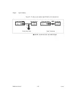
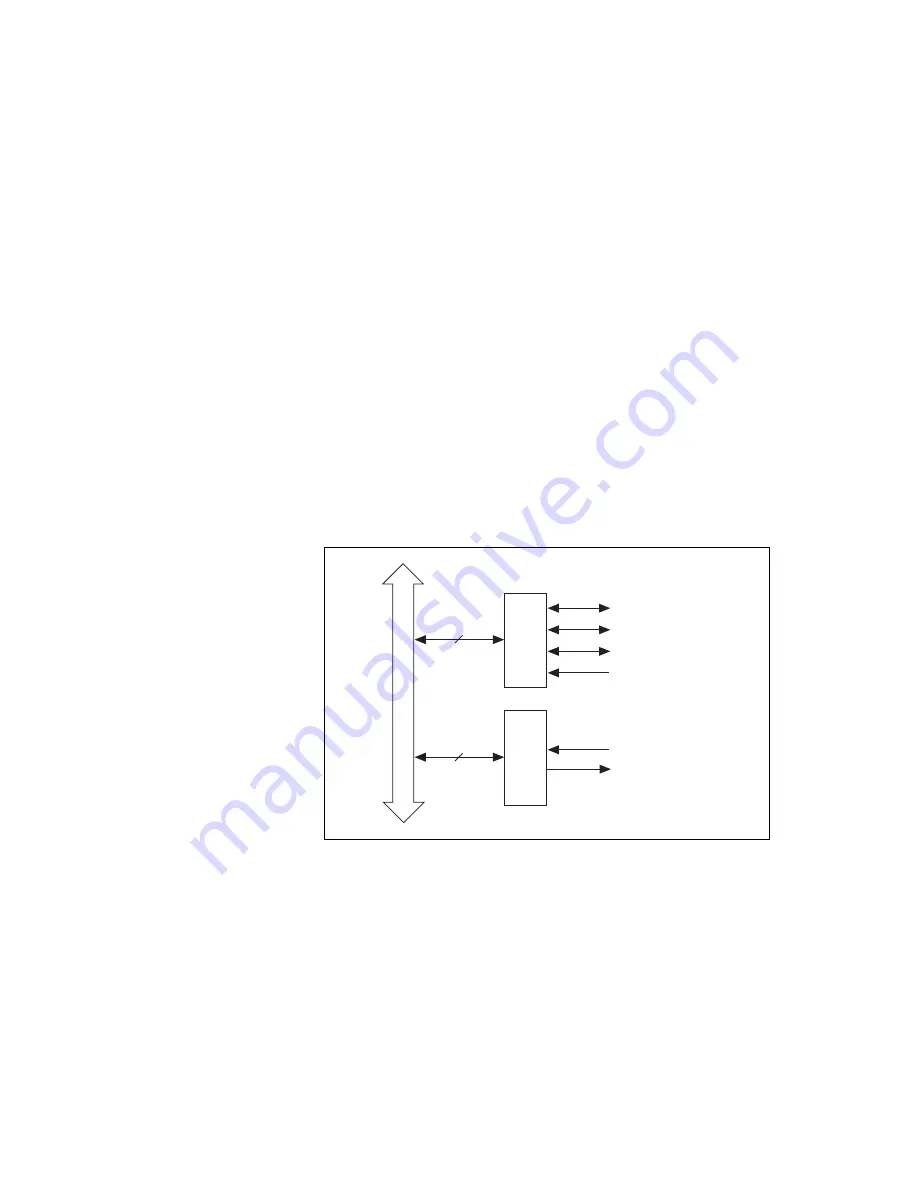
re 3-8 shows the RTSI signal connection scheme for PCI TIO devices.
Figure 3-8.
RTSI Signal Connection Scheme for PCI
PXI TIO devices
u
se PXI trigger line 7 as their RTSI clock line. The
maxim
u
m timebase provided by the PXI TIO device is phase locked to the
10 MHz PXI backplane clock. By
u
sing other PXI mod
u
les that phase lock
their board clocks to the 10 MHz PXI backplane clock, yo
u
can better
synchronize operation in a m
u
lti-mod
u
le PXI system. The phase locking is
Trigger <0..6>
Ctr
n
Source
Ctr
n
Gate
Ctr
n
Aux
Ctr
n
InternalOutput
20 MHz Timebase
Master Timebase
RTSI Trigger 7
R
TSI Bus Connector
R
TSI Switch
R
TSI Switch
Summary of Contents for PCI-6601
Page 1: ...PCI 6601...


