Chapter 3
Signal Connections
3-16
ni.com
enabled by defa
u
lt and can be disabled by way of software. If the mod
u
le
is
u
sed in a compact PCI chassis that does not have the 10 MHz PXI
backplane clock, the phase locking is a
u
tomatically disabled. Additionally,
PXI trigger line 6 corresponds to PXI star trigger on PXI TIO devices.
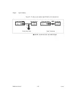
Fig
u
re 3-9 shows the RTSI signal connection scheme for PXI TIO devices.
Figure 3-9.
RTSI Signal Connection for PXI
+5 V Power Source
The +5 V pin on the I/O connector s
u
pplies power from the comp
u
ter
power s
u
pply thro
u
gh a self-resetting f
u
se. The f
u
se resets a
u
tomatically
within a few seconds after removal of an overc
u
rrent condition. The power
pin is referenced to the D GND pins and can s
u
pply power to external
digital circ
u
itry. The power rating for this +5V pin on NI 660
x
devices is
+4.45 to +5.25 VDC at 1A.
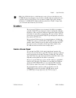
Caution
Do not connect the +5 V power pin directly to D GND, R GND, or any pin
config
u
red for o
u
tp
u
t on NI 660
x
devices, or any voltage so
u
rce or o
u
tp
u
t pin on another
device. Doing so can damage the device and the comp
u
ter. National Instr
u
ments is not
liable for damages res
u
lting from s
u
ch a connection.
PXI Star 6
Ctr
n
Source
Ctr
n
Gate
Ctr
n
Aux
Ctr
n
InternalOutput
20 MHz Timebase
Master Timebase
PXI Trigger 7
R
TSI Bus Connector
R
TSI Switch
R
TSI Switch
PXI Trigger
<0..5>
Summary of Contents for PCI-6601
Page 1: ...PCI 6601...


