background image

©

 National Instruments Corporation

5-1

NI 6238/6239 User Manual

5

Analog Output

NI 6238/6239 devices have two AO channels controlled by a single clock 
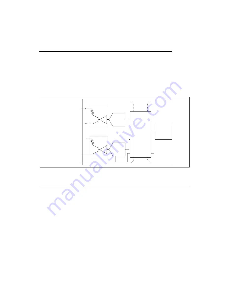
and capable of waveform generation. Figure 5-1 shows the analog current 
output circuitry of NI 6238 and NI 6239 devices.

Figure 5-1.  

NI 6238/6239 Analog Current Output Circuitry

Analog Output Circuitry

DACs

Digital-to-analog converters (DACs) convert digital codes to analog 
voltages.

V-I Converter

The V-I converter converts voltage (V) into current (I).

AO FIFO

The AO FIFO enables analog output waveform generation. It is a 
first-in-first-out (FIFO) memory buffer between the computer and the 

AO 1

AO POWER SUPPLY

DAC0

AO FIFO

Isolation

Barrier

AO 0

V-I Converter

V-I Converter

AO Sample Clock

AO GND

DAC1

Digital

Isolators

Summary of Contents for PCI-6238

Page 1: ...PCI 6238...

Page 2: ...DAQ M Series NI 6238 6239 User Manual Isolated Current Input Current Output Devices NI 6238 6239 User Manual July 2006 371913A 01...

Page 3: ...orea 82 02 3451 3400 Lebanon 961 0 1 33 28 28 Malaysia 1800 887710 Mexico 01 800 010 0793 Netherlands 31 0 348 433 466 New Zealand 0800 553 322 Norway 47 0 66 90 76 60 Poland 48 22 3390150 Portugal 35...

Page 4: ...duced or transmitted in any form electronic or mechanical including photocopying recording storing in an information retrieval system or translating in whole or in part without the prior written conse...

Page 5: ...NATIONAL INSTRUMENTS PRODUCTS ARE INCORPORATED IN A SYSTEM OR APPLICATION INCLUDING WITHOUT LIMITATION THE APPROPRIATE DESIGN PROCESS AND SAFETY LEVEL OF SUCH SYSTEM OR APPLICATION...

Page 6: ...Specifications xvii Training Courses xvii Technical Support on the Web xvii Chapter 1 Getting Started Installing NI DAQmx 1 1 Installing Other Software 1 1 Installing the Hardware 1 1 Device Pinouts 1...

Page 7: ...t Triggering 4 11 Field Wiring Considerations 4 11 Analog Input Timing Signals 4 12 AI Sample Clock Signal 4 15 Using an Internal Source 4 16 Using an External Source 4 16 Routing AI Sample Clock Sign...

Page 8: ...tput Timing Signals 5 5 AO Start Trigger Signal 5 5 Using a Digital Source 5 6 Routing AO Start Trigger Signal to an Output Terminal 5 6 AO Pause Trigger Signal 5 6 Using a Digital Source 5 7 Routing...

Page 9: ...1b Measure Low Frequency with One Counter Averaged 7 11 Method 2 Measure High Frequency with Two Counters 7 12 Method 3 Measure Large Range of Frequencies Using Two Counters 7 13 Choosing a Method fo...

Page 10: ...n HW Arm Input 7 30 Counter n Internal Output and Counter n TC Signals 7 30 Routing Counter n Internal Output to an Output Terminal 7 30 Frequency Output Signal 7 30 Routing Frequency Output to a Ter...

Page 11: ...rs Digital Isolation 9 2 Benefits of an Isolated DAQ Device 9 2 Reducing Common Mode Noise 9 3 Chapter 10 Digital Routing and Clock Generation Clock Routing 10 1 80 MHz Timebase 10 2 20 MHz Timebase 1...

Page 12: ...t Memory Access DMA 11 3 Interrupt Request IRQ 11 4 Programmed I O 11 4 Changing Data Transfer Methods between DMA and IRQ 11 4 Chapter 12 Triggering Triggering with a Digital Source 12 1 Appendix A D...

Page 13: ...inal action The sequence File Page Setup Options directs you to pull down the File menu select the Page Setup item and select Options from the last dialog box This icon denotes a tip which alerts you...

Page 14: ...nd where applicable version 7 0 or later of the NI application software NI DAQ The DAQ Getting Started Guide describes how to install your NI DAQmx for Windows software your NI DAQmx supported DAQ dev...

Page 15: ...ence Help contains VI reference and general information about measurement concepts In LabVIEW select Help NI DAQmx Base VI Reference Help The NI DAQmx Base C Reference Help contains C reference and ge...

Page 16: ...g an NI DAQmx Measurement in LabWindows CVI which includes step by step instructions about creating a measurement task using the DAQ Assistant In LabWindows CVI select Help Contents then select Using...

Page 17: ...s of the printed device documents You can find view and or print the documents for each device using the Device Document Browser at any time by inserting the CD After installing the Device Document Br...

Page 18: ...must install the software you plan to use with the device Installing NI DAQmx The DAQ Getting Started Guide which you can download at ni com manuals offers NI DAQmx users step by step instructions for...

Page 19: ...ifications available on the NI DAQ Device Document Browser or ni com manuals for more detailed information on NI 6238 6239 devices Device Accessories and Cables NI offers a variety of accessories and...

Page 20: ...ming software and PC The following sections cover the components of a typical DAQ system Figure 2 1 Components of a Typical DAQ System DAQ Hardware DAQ hardware digitizes input signals performs D A co...

Page 21: ...Os Generation and routing of RTSI signals for multi device synchronization Generation and routing of internal and external timing signals Two flexible 32 bit counter timer modules with hardware gating...

Page 22: ...trical signals to measure physical phenomena such as temperature force sound or light Some commonly used sensors are strain gauges thermocouples thermistors angular encoders linear encoders and resist...

Page 23: ...ications However if you want to develop your own cable the following kits can assist you TB 37F 37SC 37 pin solder cup terminals shell with strain relief TB 37F 37CP 37 pin crimp poke terminals shell...

Page 24: ...tware configuration Refer to the DAQ Getting Started Guide for more information about the two drivers NI DAQmx includes a collection of programming examples to help you get started developing an appli...

Page 25: ...rent return point AI GND and AO GND are connected on the device Note AI GND and AO GND are isolated from earth ground chassis ground P0 GND and P1 GND AI 0 7 AI GND Input Analog Input Channels 0 to 7...

Page 26: ...n output directional PFI terminal or a digital output terminal As a PFI output you can route many different internal AI or AO timing signals to each PFI terminal You also can route the counter timer o...

Page 27: ...ock Generation for information on the RTSI connector CAL External Calibration Positive Reference CAL supplies the positive reference during external calibration of the NI 6238 6239 CAL External Calibr...

Page 28: ...Analog Current Input Signals section Also refer to Appendix A Device Specific Information for device I O connector pinouts MUX Each M Series device has one analog to digital converter ADC The multiple...

Page 29: ...ices can perform both single and multiple A D conversions of a fixed or infinite number of samples A large first in first out FIFO buffer holds data during AI acquisitions to ensure that no data is lo...

Page 30: ...ut of range For more information on programming these settings refer to the NI DAQmx Help or the LabVIEW 8 x Help Table 4 1 shows the input ranges and resolutions supported by the NI 6238 and NI 6239...

Page 31: ...3 ties the AI input to AI GND When measuring current up to 20 mA this type of connection ensures that the voltage level on both the positive and negative side are within the common mode input range f...

Page 32: ...ltage levels provided that the common mode input range requirement is satisfied For example in Figure 4 4 the node connected to AI GND can be at 50 V above the earth ground Figure 4 4 Current Measurem...

Page 33: ...ard reference the signal is measured against AI GND This measurement method is called referenced single ended RSE The name is derived from the fact that one end of the measurement the positive input o...

Page 34: ...s referred to as AI terminal configuration Configuring AI Ground Reference Settings in Software You can program channels on an M Series device to acquire with different ground references To enable mul...

Page 35: ...can increase the settling time which decreases the accuracy of your measurements To ensure fast settling times you should do the following in order of importance Use short high quality cabling Minimiz...

Page 36: ...0 ms and average the results You could acquire 500 points from each channel at a scan rate of 125 kS s Another method would be to acquire 1 000 points from each channel at a scan rate of 250 kS s Both...

Page 37: ...gnal can be generated internally on your device or provided externally Hardware timed acquisitions have several advantages over software timed acquisitions The time between samples can be much shorter...

Page 38: ...he PC buffer fast enough to keep up with the data transfer the buffer could reach an overflow condition causing an error to be generated Non Buffered In non buffered acquisitions data is read directly...

Page 39: ...the NI Developer Zone document Field Wiring and Noise Considerations for Analog Signals for more information To access this document go to ni com info and enter the info code rdfwn3 Analog Input Timi...

Page 40: ...imum scan rate to derive the Channel Clock As the scan rate increases there eventually will not be enough time to have a full 10 s of additional delay time between channel conversions and to finish ac...

Page 41: ...te one channel at 250 kS s or two channels at 125 kS s per channel illustrates the relationship Posttriggered data acquisition allows you to view only data that is acquired after a trigger event is re...

Page 42: ...e decrements until the specified number of posttrigger samples have been acquired NI 6238 6239 devices feature the following analog input timing signals AI Sample Clock Signal AI Sample Clock Timebase...

Page 43: ...e NI DAQmx Help or the LabVIEW 8 x Help for more information Using an External Source Use one of the following external signals as the source of ai SampleClock Input PFI 0 5 RTSI 0 7 PXI_STAR Note Ref...

Page 44: ...the first ai SampleClock pulse By default this delay is set to two ticks of the ai SampleClockTimebase signal When using an externally generated ai SampleClock you must ensure the clock signal is con...

Page 45: ...ng edge of ai ConvertClock With NI DAQmx the driver will choose the fastest conversion rate possible based on the speed of the A D converter and add 10 s of padding between each channel to allow for a...

Page 46: ...tion delay of PFI 0 5 Routing AI Convert Clock Signal to an Output Terminal You can route ai ConvertClock as an active low signal out to any output PFI 6 9 or RTSI 0 7 terminal PFI 0 5 terminals are f...

Page 47: ...ly the device ignores all ai ConvertClock pulses until it recognizes an ai SampleClock pulse After the device receives the correct number of ai ConvertClock pulses it ignores subsequent ai ConvertCloc...

Page 48: ...se ai ConvertClockTimebase is not available as an output on the I O connector AI Hold Complete Event Signal The AI Hold Complete Event ai HoldCompleteEvent signal generates a pulse after each A D conv...

Page 49: ...source specify a source and an edge The source can be any of the following signals Input PFI 0 5 RTSI 0 7 Counter n Internal Output PXI_STAR Note Refer to the NI 6238 6239 Specifications for the mini...

Page 50: ...r samples the DAQ device begins to look for the reference trigger condition If the reference trigger condition occurs before the DAQ device captures the specified number of pretrigger samples the DAQ...

Page 51: ...ger out to any output PFI 6 9 or RTSI 0 7 terminal AI Pause Trigger Signal You can use the AI Pause Trigger ai PauseTrigger signal to pause and resume a measurement acquisition The internal sample clo...

Page 52: ...I Applications in Software You can use the M Series device in the following analog input applications Single point analog input Finite analog input Continuous analog input You can perform these applic...

Page 53: ...I 6238 6239 Analog Current Output Circuitry Analog Output Circuitry DACs Digital to analog converters DACs convert digital codes to analog voltages V I Converter The V I converter converts voltage V i...

Page 54: ...are controls the rate at which data is generated Software sends a separate command to the hardware to initiate each DAC conversion In NI DAQmx software timed generations are referred to as on demand t...

Page 55: ...ation of an unspecified number of samples Instead of generating a set number of data samples and stopping a continuous generation continues until you stop the operation There are several different met...

Page 56: ...triggering actions Connecting Analog Current Output Signals AO 0 1 are the current output signals for AO channels 0 and 1 AO GND is the ground reference for AO 0 1 Figure 5 2 shows how to make analog...

Page 57: ...such signal connections Analog Output Timing Signals Figure 5 3 summarizes all of the timing options provided by the analog output timing engine Figure 5 3 Analog Output Timing Options NI 6238 6239 de...

Page 58: ...o can specify whether the waveform generation begins on the rising edge or falling edge of ao StartTrigger Routing AO Start Trigger Signal to an Output Terminal You can route ao StartTrigger out to an...

Page 59: ...ge of the sample clock is received as shown in Figure 5 5 Figure 5 5 ao PauseTrigger with Other Signal Source Using a Digital Source To use ao PauseTrigger specify a source and a polarity The source c...

Page 60: ...AC update begins on the rising edge or falling edge of ao SampleClock Using an Internal Source One of the following internal signals can drive ao SampleClock AO Sample Clock Timebase divided down Coun...

Page 61: ...s delay is two ticks of ao SampleClockTimebase Figure 5 6 shows the relationship of ao SampleClock to ao StartTrigger Figure 5 6 ao SampleClock and ao StartTrigger AO Sample Clock Timebase Signal The...

Page 62: ...eClock rather than ao SampleClockTimebase Getting Started with AO Applications in Software You can use an M Series device in the following analog output applications Single point on demand generation...

Page 63: ...oid these fault conditions by following these guidelines Do not connect any digital output line to any external signal source ground signal or power supply Understand the current requirements of the l...

Page 64: ...3 are referenced to P1 GND Figures 6 1 and 6 2 show P0 0 5 and P1 0 3 on the NI 6238 and the NI 6239 device respectively Digital input and output signals can range from 0 to 30 V Refer to the NI 6238...

Page 65: ...which are listed in the NI 6238 6239 Specifications can damage the DAQ device and the computer NI is not liable for any damage resulting from such signal connections Logic Conventions With NI 6238 62...

Page 66: ...ices in the following digital I O applications Static digital input Static digital output Note For more information about programming digital I O applications and triggers in software refer to the NI...

Page 67: ...and one frequency generator as shown in Figure 7 1 The general purpose counter timers can be used for many measurement and pulse generation applications Caution When making measurements take into acco...

Page 68: ...Counter 0 Source Counter 0 Timebase Counter 0 Aux Counter 0 HW Arm Counter 0 A Counter 0 B Counter 0 Up_Down Counter 0 Z Counter 0 Gate Counter 0 Internal Output Counter 0 TC Input Selection Muxes Fr...

Page 69: ...nput after the counter is armed On demand refers to the fact that software can read the counter contents at any time without disturbing the counting process Figure 7 2 shows an example of single point...

Page 70: ...eturned are the cumulative counts since the counter armed event That is the sample clock does not reset the counter You can route the counter sample clock to the Gate input of the counter You can conf...

Page 71: ...edge on Gate Notice that if you are using an external signal as the Source at least one Source pulse should occur between each active edge of the Gate signal This condition ensures that correct values...

Page 72: ...the counter is armed while a pulse train is in progress If a counter is armed while the pulse is in the active state it will wait for the next transition to the active state to begin the measurement S...

Page 73: ...If this condition is not met consider using duplicate count prevention For information on connecting counter signals refer to the Default Counter Terminals section Period Measurement In period measur...

Page 74: ...urement is similar to single period measurement but buffered period measurement measures multiple periods The counter counts the number of rising or falling edges on the Source input between each pair...

Page 75: ...ter measures a semi period on its Gate input signal after the counter is armed A semi period is the time between any two consecutive edges on the Gate input You can route an internal or external perio...

Page 76: ...mi Period Measurement Note that if you are using an external signal as the Source at least one Source pulse should occur between each active edge of the Gate signal This condition ensures that correct...

Page 77: ...everal periods of your signal using a known timebase This method is good for low to medium frequency signals You can route the signal to measure F1 to the Gate of a counter You can route a known timeb...

Page 78: ...n generate the pulse externally and connect it to a PFI or RTSI terminal You only need to use one counter if you generate the pulse externally Route the signal to measure F1 to the Source of the count...

Page 79: ...ong pulse using the signal to measure You then measure the long pulse with a known timebase The M Series device can measure this long pulse more accurately than the faster input signal You can route t...

Page 80: ...fore the frequency of F1 is given by F1 F2 N J Choosing a Method for Measuring Frequency The best method to measure frequency depends on several factors including the expected frequency of the signal...

Page 81: ...nal to measure decreases At very low frequencies Method 2 may be too inaccurate for your application Another disadvantage of Method 2 is that it requires two counters if you cannot provide an external...

Page 82: ...1 X2 or X4 encoding A quadrature encoder can have up to three channels channels A B and Z X1 Encoding When channel A leads channel B in a quadrature cycle the counter increments When channel B leads c...

Page 83: ...ng Whether the counter increments or decrements depends on which channel leads the other Each cycle results in four increments or decrements as shown in Figure 7 17 Figure 7 17 X4 Encoding Channel Z B...

Page 84: ...hase is true and channel Z is high Incrementing and decrementing takes priority over reloading Thus when the channel B goes low to enter the reload phase the increment occurs first The reload occurs w...

Page 85: ...tive edge on the Gate input The counter stores the count in a hardware save register You can configure the rising or falling edge of the Aux input to be the active edge You can configure the rising or...

Page 86: ...of the Aux signal The counter then stores the count in a hardware save register On the next active edge of the Gate signal the counter begins another measurement A DMA controller transfers the stored...

Page 87: ...of a pulse with a pulse delay of four and a pulse width of three using the rising edge of Source Figure 7 22 Single Pulse Generation Single Pulse Generation with Start Trigger The counter can output a...

Page 88: ...se You also can specify the pulse width The delay and pulse width are measured in terms of a number of active edges of the Source input The counter ignores the Gate input while a pulse generation is i...

Page 89: ...r falling The counter can begin the pulse train generation as soon as the counter is armed or in response to a hardware Start Trigger You can route the Start Trigger to the Gate input of the counter Y...

Page 90: ...Frequency Output signal The Frequency Output signal is the Frequency Output Timebase divided by a number you select from 1 to 16 The Frequency Output Timebase can be either the 20 MHz Timebase divided...

Page 91: ...een the Gate and the pulse on the output by a specified amount Thus the delay between the Gate and the pulse produced successively increases Note ETS Equivalent Time Sampling The increase in the delay...

Page 92: ...e the following counter timing signals Counter n Source Counter n Gate Counter n Aux Counter n A Counter n B Counter n Z Counter n Up_Down Counter n HW Arm Counter n Internal Output Counter n TC Frequ...

Page 93: ...Gate can be routed to Counter 0 Source Counter 0 TC or Counter 0 Gate can be routed to Counter 1 Source Some of these options may not be available in some driver software Routing Counter n Source to a...

Page 94: ...R In addition Counter 1 Internal Output or Counter 1 Source can be routed to Counter 0 Gate Counter 0 Internal Output or Counter 0 Source can be routed to Counter 1 Gate Some of these options may not...

Page 95: ...s or measuring two pulse encoders Routing Signals to A B and Z Counter Inputs Each counter has independent input selectors for each of the A B and Z inputs Any of the following signals can be routed t...

Page 96: ...tput can be routed to Counter 0 HW Arm Counter 0 Internal Output can be routed to Counter 1 HW Arm Some of these options may not be available in some driver software Counter n Internal Output and Coun...

Page 97: ...NI DAQmx Help or the LabVIEW 8 x Help for more information on how to connect your signals for common counter measurements and generations M Series default PFI lines for counter functions are listed i...

Page 98: ...generation After a continuous generation has triggered the pulses continue to generate until you stop the operation in software For finite generations the specified number of pulses is generated and...

Page 99: ...ed your device samples the input on each rising edge of a filter clock M Series devices use an onboard oscillator to generate the filter clock with a 40 MHz frequency Note NI DAQmx only supports filte...

Page 100: ...with M Seriesand CompactDAQ for more information about digital filters and counters To access this KnowledgeBase go to ni com info and enter the info code rddfms Prescaling Prescaling allows the coun...

Page 101: ...the counter Source is one of the internal timebases 80MHzTimebase 20MHzTimebase or 100kHzTimebase Duplicate Count Prevention Duplicate count prevention or synchronous counting mode ensures that a coun...

Page 102: ...urce pulse In this example the counter stores the values in the buffer on the first rising Source edge after the rising edge of Gate The details of when exactly the counter synchronizes the Gate signa...

Page 103: ...unt to be stored in the buffer even if no Source edges occur between Gate signals as shown in Figure 7 33 Figure 7 33 Duplicate Count Prevention Example Even if the Source pulses are long the counter...

Page 104: ...uplicate count prevention Enabling Duplicate Count Prevention in NI DAQmx You can enable duplicate count prevention in NI DAQmx by setting the Enable Duplicate Count Prevention attribute property For...

Page 105: ...In other internal source mode the device synchronizes signals on the falling edge of the source and counts on the following rising edge of the source as shown in Figure 7 35 Table 7 6 Synchronization...

Page 106: ...ice generates a delayed Source signal by delaying the Source signal by several nanoseconds The device synchronizes signals on the rising edge of the delayed Source signal and counts on the following r...

Page 107: ...Caution When making measurements take into account the minimum pulse width and time delay of the digital input and output lines Figure 8 1 shows the circuitry of one PFI input line Each PFI line is si...

Page 108: ...as Timing Input Signals Use PFI 0 5 terminals to route external timing signals to many different M Series functions Each input PFI terminal can be routed to any of the following signals AI Convert Cl...

Page 109: ...observable by the user or another instrument Refer to the Digital Output Port 1 section of the NI 6238 6239 Specifications for more information Using PFI Terminals as Static Digital Inputs and Outputs...

Page 110: ...ote NI DAQmx only supports filters on counter inputs The following is an example of low to high transitions of the input signal High to low transitions work similarly Assume that an input terminal has...

Page 111: ...tered version of the input signal Refer to the KnowledgeBase document Digital Filtering with M Series and CompactDAQ for more information about digital filters and counters To access this KnowledgeBas...

Page 112: ...de of its normal operating range Treat the DAQ device as you would treat any static sensitive device Always properly ground yourself and the equipment when handling the DAQ device or connecting to it...

Page 113: ...apter 8 PFI National Instruments Corporation 8 7 NI 6238 6239 User Manual Figure 8 5 NI 6238 Digital I O Connections DO Source P1 0 3 P1 VCC P1 0 P1 1 P1 GND P0 0 P0 GND P1 GND P0 GND Digital Isolator...

Page 114: ...g the maximum input voltage or maximum working voltage ratings which are listed in the NI 6238 6239 Specifications can damage the DAQ device and the computer NI is not liable for any damage resulting...

Page 115: ...cuitry RTSI digital routing and clock generation are all referenced to a non isolated ground Refer to Table 9 1 for an example of the symbols for isolated ground and non isolated ground Figure 9 1 Gen...

Page 116: ...digital isolators Unlike analog isolators digital isolators do not introduce any analog error in the measurements taken by the device The A D converter used for analog input is on the isolated side o...

Page 117: ...returning to the non isolated side which is earth ground These parasitic currents interact with parasitic and non parasitic resistances causing voltage spikes These voltage spikes are called common mo...

Page 118: ...he acquisition generation sub systems use these signals to manage acquisitions and generations These signals can come from the following sources Your M Series device Other devices in your system throu...

Page 119: ...imebase by dividing down the 80 MHz Timebase 100 kHz Timebase The 100 kHz Timebase can be used to generate many of the AI and AO timing signals The 100 kHz Timebase also can be used as the Source inpu...

Page 120: ...e initiator device receive the 10 MHz Reference Clock from RTSI This signal becomes the external reference clock A PLL on each device generates the internal timebases synchronous to the external refer...

Page 121: ...y as five DAQ vision motion or CAN devices in the computer In a PXI system the RTSI bus consists of the RTSI bus interface and the PXI trigger signals on the PXI backplane This bus can route timing an...

Page 122: ...igger ao SampleClock ao StartTrigger ao PauseTrigger 10 MHz Reference Clock Counter n Source Gate Z Internal Output FREQ OUT Input PFI 0 5 Note Signals with a are inverted before being driven on the R...

Page 123: ...input is edge or level sensitive RTSI Filters You can enable a programmable debouncing filter on each PFI RTSI or PXI_STAR signal When the filters are enabled your device samples the input on each ri...

Page 124: ...ies device does not use the filtered version of the input signal Refer to the KnowledgeBase document Digital Filtering with M Series and CompactDAQ for more information about digital filters and count...

Page 125: ...documentation for your chassis for details PXI_STAR Trigger In a PXI system the Star Trigger bus implements a dedicated trigger line between the first peripheral slot adjacent to the system slot and t...

Page 126: ...The value of N depends on the filter setting refer to Table 10 3 The filter setting for each input can be configured independently On power up the filters are disabled Figure 10 4 shows an example of...

Page 127: ...r a RTSI input is routed directly to PFI the M Series device does not use the filtered version of the input signal Refer to the KnowledgeBase document Digital Filtering with M Series and CompactDAQ fo...

Page 128: ...rface DMA Controllers NI 6238 6239 devices have four fully independent DMA controllers for high performance transfers of data blocks One DMA controller is available for each measurement and acquisitio...

Page 129: ...hassis PXI specifications are developed by the PXI System Alliance www pxisa org Using the terminology of the PXI specifications NI PXI 6238 6239 devices are 3U Hybrid Slot Compatible PXI 1 Peripheral...

Page 130: ...I chassis adhering to the PICMG CompactPCI 2 0 R3 0 core specification PXI specific features are implemented on the J2 connector of the CompactPCI bus The PXI device is compatible with any CompactPCI...

Page 131: ...ism where the user s program is responsible for transferring data Each read or write call in the program initiates the transfer of data Programmed I O is typically used in software timed on demand ope...

Page 132: ...ing sections The Analog Input Triggering section of Chapter 4 Analog Input The Analog Output Triggering section of Chapter 5 Analog Output The Counter Triggering section of Chapter 7 Counters Triggeri...

Page 133: ...9 User Manual 12 2 ni com You also can program your DAQ device to perform an action in response to a trigger from a digital source The action can affect the following Analog input acquisition Analog o...

Page 134: ...ory choices and other information for the NI 6238 and NI 6239 M Series isolated devices To obtain documentation for devices not listed here refer to ni com manuals NI 6238 NI 6238 Pinout Figure A 1 sh...

Page 135: ...P0 1 CTR 0 B 33 PFI 2 P0 2 CTR 1 SRC 15 PFI 3 P0 3 CTR 1 GATE 34 PFI 4 P0 4 CTR 1 AUX 16 PFI 5 P0 5 1 2 3 4 5 6 7 8 9 10 11 12 13 14 15 16 17 18 19 20 21 22 23 24 25 26 27 28 29 30 31 32 33 34 35 36 3...

Page 136: ...crew terminal connector blocks Use an SH37F 37M cable to connect an NI 6238 device to a connector block such as the following CB 37F HVD 37 pin DIN rail screw terminal block UL Recognized derated to 3...

Page 137: ...able UL Listed derated to 30 Vrms 42 4 Vpk or 60 VDC R37F 37M 1 37 pin female to male ribbon I O cable SH37F P 4 37 pin female to pigtails shielded I O cable Custom Cabling and Connectivity Refer to t...

Page 138: ...0 Z 32 PFI 1 P0 1 CTR 0 B 33 PFI 2 P0 2 CTR 1 SRC 15 PFI 3 P0 3 CTR 1 GATE 34 PFI 4 P0 4 CTR 1 AUX 16 PFI 5 P0 5 1 2 3 4 5 6 7 8 9 10 11 12 13 14 15 16 17 18 19 20 21 22 23 24 25 26 27 28 29 30 31 32...

Page 139: ...onnector blocks Use an SH37F 37M cable to connect an NI 6239 device to a connector block such as the following CB 37F HVD 37 pin DIN rail screw terminal block UL Recognized derated to 30 Vrms 42 4 Vpk...

Page 140: ...ed Cables In most applications you can use the following cables SH37F 37M x 37 pin female to male shielded I O cable UL Listed derated to 30 Vrms 42 4 Vpk or 60 VDC R37F 37M 1 37 pin female to male ri...

Page 141: ...to AI 1 is high enough the resulting reading can somewhat affect the voltage in AI 0 To circumvent this problem use a voltage follower that has operational amplifiers op amps with unity gain for each...

Page 142: ...ation 1 convert period convert rate This method allows multiple channels to be sampled relatively quickly in relationship to the overall sample rate providing a nearly simultaneous effect with a fixed...

Page 143: ...Why Duplicate count prevention ensures that the counter returns correct data for counter measurement in some applications where a slow or non periodic external source is used Refer to the Duplicate Co...

Page 144: ...nstruments Application Engineers make sure every question receives an answer For information about other technical support options in your area visit ni com services or contact your local office at ni...

Page 145: ...om calibration If you searched ni com and could not find the answers you need contact your local office or NI corporate headquarters Phone numbers for our worldwide offices are listed at the front of...

Page 146: ...o Per Degree Ohm A A Amperes the unit of electric current A D Analog to Digital Most often used as A D converter AC Alternating current accuracy A measure of the capability of an instrument or sensor...

Page 147: ...pecific level on either an increasing or a decreasing signal positive or negative slope Analog triggering can be implemented either in software or in hardware When implemented in software LabVIEW all...

Page 148: ...f a program or algorithm BNC Bayonet Neill Concelman A type of coaxial connector used in situations requiring shielded cable for signal connections and or controlled impedance applications buffer 1 Te...

Page 149: ...rejection The ability of an electronic system to cancel any electronic noise pick up that is common to both the positive and negative polarities of the input leads to the instrument front end Common...

Page 150: ...attern which is fed to the DAC DAQ 1 Data acquisition The process of collecting and measuring electrical signals from sensors transducers and test probes or fixtures and inputting them to a computer f...

Page 151: ...peaks of current many different types of DC measurements are made including DC Voltage DC current and DC power device A plug in data acquisition product card or pad that can contain multiple channels...

Page 152: ...and I O devices independently of the CPU driver Software unique to the device or type of device and includes the set of commands the device accepts E edge detection A technique that locates an edge of...

Page 153: ...m data can be stored on the FIFO ahead of time This again reduces the effect of latencies associated with getting the data from system memory to the DAQ device filter A physical device or digital algo...

Page 154: ...Normally a noncurrent carrying circuit intended for safety 3 A common reference point for an electrical system H hardware The physical components of a computer system such as the circuit boards plug...

Page 155: ...rchannel delay must be short enough to allow sampling of all the channels in the channel list within the sample interval The greater the interchannel delay the more time the PGIA is allowed to settle...

Page 156: ...ve determination of a physical characteristic In practice measurement is the conversion of a physical quantity or observation to a domain where a human being or computer can determine the value measur...

Page 157: ...iplexer A set of semiconductor or electromechanical switches arranged to select one of many inputs to a single output The majority of DAQ cards have a multiplexer on the input which permits the select...

Page 158: ...ansion bus architecture originally developed by Intel to replace ISA and EISA It offers a theoretical maximum transfer rate of 132 MB s period The period of a signal most often measured from one zero...

Page 159: ...s PCI Express eXtensions for Instrumentation The PXI implementation of PCI Express a scalable full simplex serial bus standard that operates at 2 5 Gbps and offers both asynchronous and isochronous da...

Page 160: ...ional Instruments timing bus that connects DAQ devices directly by means of connectors on top of the devices for precise synchronization of functions S s Seconds S Samples sample counter The clock tha...

Page 161: ...orms they are most often converted to electronic form for measurement single trigger mode When the arbitrary waveform generator goes through the staging list only once single buffered Describes a devi...

Page 162: ...I DAQmx a collection of one or more channels timing and triggering and other properties that apply to the task itself Conceptually a task represents a measurement or generation you want to perform TC...

Page 163: ...period tsp Source pulse width TTL Transistor Transistor Logic A digital circuit composed of bipolar transistors wired in a certain manner A typical medium speed digital technology Nominal TTL logic le...

Page 164: ...tion G 19 NI 6238 6239 User Manual Vs Signal source voltage virtual channel See channel W waveform 1 The plot of the instantaneous amplitude of a signal as a function of time 2 Multiple voltage readin...

Page 165: ...signal 4 17 AI Start Trigger signal 4 21 AI timing signals 4 12 ai ConvertClock 4 18 ai ConvertClockTimebase 4 21 ai HoldCompleteEvent 4 21 ai PauseTrigger 4 24 ai ReferenceTrigger 4 22 ai SampleClock...

Page 166: ...erface 11 1 RTSI 10 3 C cables 2 4 A 3 A 6 choosing for your device 1 2 custom 2 4 calibration certificate NI resources C 2 calibration circuitry 2 3 cascading counters 7 33 changing data transfer met...

Page 167: ...7 3 filters 7 33 generation 7 21 input applications 7 3 other features 7 33 output applications 7 21 prescaling 7 34 pulse train generation 7 23 retriggerable single pulse generation 7 22 simple pulse...

Page 168: ...NI DAQmx 7 38 example 7 37 troubleshooting B 3 E edge counting 7 3 buffered 7 4 non cumulative buffered 7 5 sample clock 7 4 edge separation measurement buffered two signal 7 20 single two signal 7 19...

Page 169: ...erminals as 8 2 using RTSI terminals as 10 6 installation hardware 1 1 NI DAQ 1 1 other software 1 1 instrument drivers NI resources C 1 interface bus 11 1 interrupt request as a transfer method 11 4...

Page 170: ...ation xv NI DAQmx enabling duplicate count prevention 7 38 non buffered hardware timed acquisitions 4 11 generations 5 3 non cumulative buffered edge counting 7 5 O other internal source mode 7 39 oth...

Page 171: ...ignals 10 6 S sample clock edge counting 7 4 scanning speed 4 9 semi period measurement 7 9 buffered 7 10 single 7 9 sensors 2 3 settings analog input ground reference 4 5 short high quality cabling 4...

Page 172: ...ing PFI terminals as 8 3 support technical C 1 synchronization modes 7 38 80 MHz source 7 39 external source 7 40 other internal source 7 39 synchronizing multiple devices 10 3 synchronous counting mo...

Page 173: ...Os 8 3 as timing input 8 2 to export timing output signals 8 3 using RTSI as outputs 10 5 terminals as timing input signals 10 6 using short high quality cabling 4 8 V V I Converter 5 1 W waveform ge...

Reviews: