background image

Chapter 3

Hardware Overview

NI 6115/6120 User Manual

3-10

ni.com

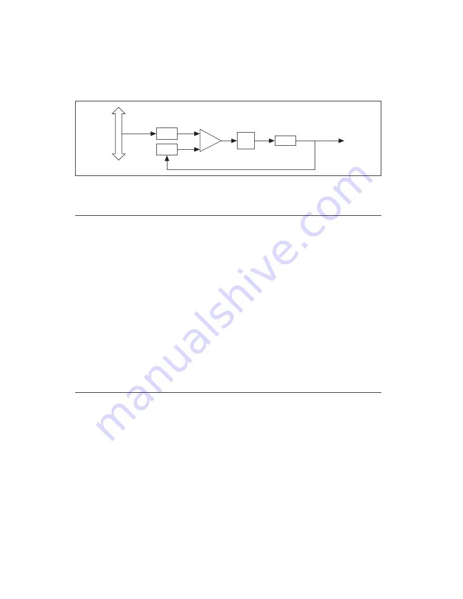
Figure 3-10.  

PLL Block Diagram

Correlated Digital I/O

The NI 6115/6120 contains eight lines of DIO for general-purpose use. 
You can software-configure groups of individual lines for either input or 
output. The NI 6115/6120 includes a FIFO for buffered operation. This 
operation allows you to read/write an array of data, using either an internal 
or external clock source, at a maximum rate of 10 MHz. In addition, you 
can correlate DIO and AI/AO operations to the same clock. Refer to the 

Correlating DIO Signal Connections

 section of Chapter 4

Connecting 

Signals

, for information on which signals you can use to clock DIO 

operation. At system startup and reset, the DIO ports are all 
high-impedance.

The hardware up/down control for general-purpose counters 0 and 1 are 
connected onboard to DIO6 and DIO7, respectively. Thus, you can use 
DIO6 and DIO7 to control the general-purpose counters. The up/down 
control signals, GPCTR0_UP_DOWN and GPCTR1_UP_DOWN, are 
input only and do not affect the operation of the DIO lines.

Timing Signal Routing

The DAQ-STC provides a flexible interface for connecting timing signals 
to other devices or external circuitry. The NI 6115/6120 uses the RTSI bus 
to interconnect timing signals between devices, and it uses the 
programmable function input (PFI) pins on the I/O connector to connect the 
device to external circuitry. These connections are designed to enable the 
NI 6115/6120 to both control and be controlled by other devices and 
circuits.

There are 13 timing signals internal to the DAQ-STC that can be controlled 
by an external source. These timing signals can also be controlled by 
signals generated by the DAQ-STC, and these selections are fully software 

Phase Comp

Div/10

Div/60

VCXO

60 MHz out

synched to 10 MHZ

backplane clock

Loop
Filter

+

PXI Bus

10 MHz

Summary of Contents for NI 6115/6120

Page 1: ...DAQ NI 6115 6120 User Manual Multifunction I O Devices for PCI PXI CompactPCI Bus Computers NI 6115 6120 User Manual November 2002 Edition Part Number 322812C 01...

Page 2: ...8 14 24 24 Germany 089 741 31 30 Greece 01 42 96 427 Hong Kong 2645 3186 India 91 80 4190000 Israel 03 6393737 Italy 02 413091 Japan 03 5472 2970 Korea 02 3451 3400 Malaysia 603 9596711 Mexico 001 800...

Page 3: ...ion operation or maintenance instructions owner s modification of the product owner s abuse misuse or negligent acts and power failure or surges fire flood accident actions of third parties or other e...

Page 4: ...ruments could void the user s authority to operate the equipment under the FCC Rules Class A Federal Communications Commission This equipment has been tested and found to comply with the limits for a...

Page 5: ...ncludes a DoC for most every hardware product except for those bought for OEMs if also available from an original manufacturer that also markets in the EU or where compliance is not required as for el...

Page 6: ...ents ADE Software 1 5 Optional Equipment 1 6 Custom Cabling 1 6 Unpacking 1 7 Safety Information 1 8 Chapter 2 Installing and Configuring the NI 6115 6120 Installing the Software 2 1 Installing the Ha...

Page 7: ...13 Connecting Analog Output Signals 4 14 Connecting Digital I O Signals 4 15 Correlating DIO Signal Connections 4 16 Power Connections 4 18 Connecting Timing Signals 4 18 Programmable Function Input...

Page 8: ...4 37 FREQ_OUT Signal 4 38 Field Wiring Considerations 4 39 Chapter 5 Calibration Loading Stored Calibration Constants 5 1 Self Calibration 5 2 External Calibration 5 2 Appendix A Specifications Append...

Page 9: ...le brackets that contain numbers separated by an ellipsis represent a range of values associated with a bit or signal name for example DIO 3 0 The symbol leads you through nested menu items and dialog...

Page 10: ...family PCI Peripheral Component Interconnect PCI is a high performance expansion bus architecture originally developed by Intel to replace ISA and EISA PXI A rugged open system for modular instrumenta...

Page 11: ...are using accessory products read the terminal block and cable assembly installation guides They explain how to physically connect the relevant pieces of the system Consult these guides when you are m...

Page 12: ...e by the NI MITE bus interface chip that connects the device to the PXI or PCI I O bus The MITE implements the PCI Local Bus Specification so that you can configure all the interrupts and base memory...

Page 13: ...sic plug in device functions For example the RTSI interface on the NI PXI 6115 6120 is available in a PXI chassis but not in a CompactPCI chassis The CompactPCI specification permits vendors to develo...

Page 14: ...115 NI PXI 6115 NI PCI 6120 NI PXI 6120 NI 6115 6120 User Manual NI DAQ for PC compatibles Optional One of the following software packages and documentation LabVIEW Windows Measurement Studio Windows...

Page 15: ...ctions that you can call from the ADE These functions allow you to use all the features of the device NI DAQ carries out many of the complex interactions such as programming interrupts between the com...

Page 16: ...or using LabVIEW with National Instruments DAQ hardware is included with LabVIEW LabWindows CVI is a complete ANSI C ADE that features an interactive user interface code generation tools and the LabWi...

Page 17: ...the development time for your data acquisition and control application Optional Equipment NI offers a variety of products to use with the NI 6115 6120 including cables connector blocks and other acces...

Page 18: ...Honda backshell Unpacking The NI 6115 6120 is shipped in an antistatic package to prevent electrostatic damage to the device Electrostatic discharge ESD can damage several components on the device Ca...

Page 19: ...sh The product must be completely dry and free from contaminants before you return it to service Operate the product only at or below Pollution Degree 2 Pollution is foreign matter in a solid liquid o...

Page 20: ...tribution such as that provided by a standard wall outlet for example 115 V for U S or 230 V for Europe Examples of Installation Category II are measurements performed on household appliances portable...

Page 21: ...tical to the pinout for the NI 6115 6120 Note It is important to install NI DAQ before installing the NI 6115 6120 to ensure that the device is properly detected Installing the Hardware You can instal...

Page 22: ...fully insert the device into the chassis 8 Screw the front panel of the NI PXI 6115 6120 to the front panel mounting rail of the system 9 Visually verify the installation Make sure the device is not t...

Page 23: ...s with no user interaction Bus related configuration includes setting the device base memory address and interrupt channel The NI PXI 6115 6120 is fully compatible with the industry standard PXI Speci...

Page 24: ...Trigger Counter Timing I O RTSI Bus Interface DMA IRQ Bus Interface DAC FIFO Address Data Control Data 32 Analog Input Control EEPROM Control DMA Interface FPGA DAQ STC Bus Interface Analog Output Con...

Page 25: ...PROM CH0 Amplifier Calibration Mux AI CH0 Mux Analog Trigger Circuitry 2 Trigger Level DACs Trigger Calibration DACs DAC1 DAQ STC Analog Input Timing Control Analog Output Timing Control Digital I O T...

Page 26: ...accommodate It has ranges of 42 V 20 V 10 V 5 V 2 V 1 V 500 mV and 200 mV and is suited for a wide variety of signal levels By choosing the optimal gain setting you can maximize usage of the dynamic...

Page 27: ...e DC offset for the input amplifier and amplify only the AC component This configuration effectively uses the dynamic range of the ADC The input impedance for the programmable gain instrumentation amp...

Page 28: ...a direct analog input from the PFI0 TRIG1 pin on the I O connector or a post gain signal from the output of the PGIA on any of the channels as shown in Figure 3 3 The trigger level range for the direc...

Page 29: ...hValue is unused Figure 3 4 Below Low Level Analog Triggering Mode In above high level analog triggering mode the trigger is generated when the signal value is greater than highValue as shown in Figur...

Page 30: ...nal value is between the lowValue and the highValue as Figure 3 6 shows Figure 3 6 Inside Region Analog Triggering Mode In high hysteresis analog triggering mode the trigger is generated when the sign...

Page 31: ...outputs whenever the AI signal crosses a specific threshold Antialiasing Filters Each AI channel on the NI 6115 6120 is equipped with a programmable antialaising Bessel filter On the NI 6115 you can p...

Page 32: ...PLL circuitry consists of a voltage controlled crystal oscillator VCXO with a tuning range of 50 ppm The VCXO generates the 60 MHz master clock used onboard the NI PXI 6115 6120 The PLL locks to the 1...

Page 33: ...e connected onboard to DIO6 and DIO7 respectively Thus you can use DIO6 and DIO7 to control the general purpose counters The up down control signals GPCTR0_UP_DOWN and GPCTR1_UP_DOWN are input only an...

Page 34: ...ows that STARTSCAN can be generated from a number of sources including the external signals RTSI 0 6 and PFI 0 9 and the internal signals Scan Interval Counter TC and GPCTR0_OUT Many of these timing s...

Page 35: ...eneral purpose signals at the I O connector The NI 6115 6120 can use either its internal 20 MHz timebase or a timebase received over the RTSI bus In addition if you configure the device to use the int...

Page 36: ...I 6 connects to the PXI Star Trigger line allowing the NI 6115 6120 to receive triggers from any Star Trigger controller plugged into slot 2 of the chassis For more information on the Star Trigger ref...

Page 37: ...als section of Chapter 4 Connecting Signals for a description of the signals shown in Figures 3 12 and 3 13 PXI Bus Connector PXI Trigger 7 DAQ STC TRIG1 TRIG2 CONVERT UPDATE WFTRIG GPCTR0_SOURCE GPCT...

Page 38: ...s Caution Connections that exceed any of the maximum ratings of input or output signals on the NI 6115 6120 can damage the device and the computer NI is not liable for any damage resulting from such s...

Page 39: ...1 10 9 8 7 6 5 4 3 2 1 ACH0 ACH1 ACH1GND ACH2 ACH3 ACH3GND NC NC NC NC NC NC DAC0OUT DAC1OUT NC DIO4 DGND DIO1 DIO6 DGND 5V OUTPUT DGND DGND PFI0 TRIG1 PFI1 TRIG2 DGND 5V OUTPUT DGND PFI5 UPDATE PFI6...

Page 40: ...annel 0 Output This pin supplies the voltage output of AO channel 0 DAC1OUT AOGND Output Analog Channel 1 Output This pin supplies the voltage output of AO channel 1 AOGND Analog Output Ground The AO...

Page 41: ...GPCTR1_SOURCE DGND Input Output PFI3 Counter 1 Source As an input this is a PFI As an output this is the GPCTR1_SOURCE signal This signal reflects the actual source connected to the general purpose co...

Page 42: ...tput FREQ_OUT DGND Output Frequency Output This output is from the frequency generator output 1 The GPCTR0_OUT acts as an input when using external clock mode with correlated DIO Table 4 3 Analog I O...

Page 43: ...hort circuit to ground 5 at 10 5 at 10 1 Applies to range 10 V impedance refers to ACH 0 3 2 Applies to range 10 V impedance refers to ACH 0 3 Table 4 5 Digital I O Signal Summary Signal Name Signal T...

Page 44: ...3 5 at VCC 0 4 5 at 0 4 1 5 50 k pu PFI4 GPCTR1_GATE DIO VCC 0 5 3 5 at VCC 0 4 5 at 0 4 1 5 50 k pu GPCTR1_OUT DO 3 5 at VCC 0 4 5 at 0 4 1 5 50 k pu PFI5 UPDATE DIO VCC 0 5 3 5 at VCC 0 4 5 at 0 4 1...

Page 45: ...ypically between 1 and 100 mV but can be much higher if power distribution circuits are not properly connected If a grounded signal source is improperly measured this difference may appear as an error...

Page 46: ...urce to a channel on the NI 6115 and NI 6120 respectively Figure 4 2 Pseudodifferential Input Connections on the NI 6115 for Ground Referenced Signals Vm ACH0 Connections Shown PGIA 100 pf 10 nf Groun...

Page 47: ...ts both the common mode noise in the signal and the ground potential difference between the signal source and the device ground shown as Vcm in Figures 4 2 and 4 3 Vm 100 pF 1 M 50 0 1 F High Frequenc...

Page 48: ...gnal source to a channel on the NI 6115 and NI 6120 respectively Figure 4 4 Differential Input Connections on the NI 6115 for Nonreferenced Signals ACH0 Connections Shown PGIA 1 M 100 pf 10 nf Bias Re...

Page 49: ...0GND This connection gives a slight measurement error due to the voltage divider formed with the output impedance of the floating source but it also gives a more balanced input for better common mode...

Page 50: ...nals of interest while rejecting common mode signals as long as the following three conditions are met 1 The common mode voltage Vcm which is equivalent to subtracting ACH 0 3 GND from ACH 0 3 and whi...

Page 51: ...output signal for AO channel 0 DAC1OUT is the voltage output signal for AO channel 1 AOGND is the ground reference signal for the AO channels AOGND is a hard ground Figure 4 6 shows how to connect AO...

Page 52: ...IO port You can program groups of individual lines to be inputs or outputs Caution Exceeding the maximum input voltage ratings which are listed in Table 4 3 can damage the NI 6115 6120 and the compute...

Page 53: ...k source AI Scan Start AO Update GPCTR RTSI 0 5 External Clock Notes To use either of the GPCTR signals or the external clock to clock DIO operations you must use one RTSI 0 5 pin To use an external c...

Page 54: ...on 4 17 NI 6115 6120 User Manual Figure 4 8 Clock Signal Driving DI and DO Signals Figure 4 9 shows a DIO operation driven by the AO Update signal on its rising edge Figure 4 9 Rising Edge AO Update S...

Page 55: ...ny other device Doing so can damage the NI 6115 6120 and the computer NI is not liable for damage resulting from such connections Connecting Timing Signals Caution Exceeding the maximum input voltage...

Page 56: ...ation signals and the General Purpose Timing Signal Connections section later in this chapter explains the general purpose timing signals All digital timing connections are referenced to DGND This ref...

Page 57: ...polarity selection for any of the timing signals but the edge or level detection depends upon the particular timing signal being controlled The detection requirements for each timing signal are listed...

Page 58: ...ion TRIG1 Signal Any PFI pin can receive as an input the TRIG1 signal which is available as an output on the PFI0 TRIG1 pin Refer to Figures 4 12 and 4 13 for the relationship of TRIG1 to the DAQ sequ...

Page 59: ...TRIG1 Output Signal Timing The device also uses TRIG1 to initiate pretriggered DAQ operations In most pretriggered applications TRIG1 is generated by a software trigger Refer to the TRIG2 signal desc...

Page 60: ...erted prior to the scan counter decrementing to zero After the selected edge of TRIG2 is received the device acquires a fixed number of scans and the acquisition stops This mode acquires data both bef...

Page 61: ...ts if you select internally triggered CONVERT As an output STARTSCAN reflects the actual start pulse that initiates a scan even if another PFI is externally triggering the starts You have two output o...

Page 62: ...RTSCAN pulses should be separated by at least one scan period A counter on the NI 6115 6120 internally generates STARTSCAN unless you select some external source This counter is started by the TRIG1 s...

Page 63: ...larity selection for either rising or falling edge The selected edge of CONVERT initiates an A D conversion As an output CONVERT reflects the actual convert pulse that is connected to the ADC even if...

Page 64: ...ff scans in a DAQ sequence You can configure the PFI pin you select as the source for AIGATE in level detection mode You can configure the polarity selection for the PFI pin for either active high or...

Page 65: ...to 100 ns after an A D conversion begins The polarity of this output is software selectable but is typically configured so that a low to high leading edge can clock external AI multiplexers indicatin...

Page 66: ...ing Waveform Generation Timing Connections The AO group defined for the NI 6115 6120 is controlled by WFTRIG UPDATE and UISOURCE WFTRIG Signal Any PFI pin can receive as an input the WFTRIG signal whi...

Page 67: ...de You can select any PFI pin as the source for UPDATE and configure the polarity selection for either rising or falling edge The selected edge of UPDATE updates the outputs of the DACs In order to us...

Page 68: ...an be stopped by software or the internal buffer counter BC D A conversions generated by either an internal or external UPDATE signal do not occur when gated by the software command register gate UISO...

Page 69: ...PCTR0_UP_DOWN GPCTR1_SOURCE GPCTR1_GATE GPCTR1_OUT GPCTR1_UP_DOWN and FREQ_OUT GPCTR0_SOURCE Signal Any PFI pin can receive as an input the GPCTR0_SOURCE signal which is available as an output on the...

Page 70: ...PCTR0_GATE signal which is available as an output on the PFI9 GPCTR0_GATE pin As an input GPCTR0_GATE is configured in the edge detection mode You can select any PFI pin as the source for GPCTR0_GATE...

Page 71: ...counter 0 You have two software selectable output options pulse on TC and toggle output polarity on TC The output polarity is software selectable for both options This output is set to high impedance...

Page 72: ...GPCTR1_SOURCE pin As an input GPCTR1_SOURCE is configured in the edge detection mode You can select any PFI pin as the source for GPCTR1_SOURCE and configure the polarity selection for either rising o...

Page 73: ...er contents As an output GPCTR1_GATE monitors the actual gate signal connected to general purpose counter 1 even if another PFI externally generates the gate This output is set to high impedance at st...

Page 74: ...e disabled so that software can control the up down functionality and leave the DIO7 pin free for general use Figure 4 36 shows the timing requirements for the GATE and SOURCE input signals and the ti...

Page 75: ...edge of the source signal If you use an internal timebase clock the gate signal cannot be synchronized with the clock In this case gates applied close to a source edge take effect either on that sourc...

Page 76: ...through areas with large magnetic fields or high electromagnetic interference Route signals to the device carefully Keep cabling away from noise sources The most common noise source in a PCI DAQ syst...

Page 77: ...and least accurate whereas the last level is the slowest most difficult and most accurate Loading Stored Calibration Constants The NI 6115 6120 is factory calibrated before shipment at approximately...

Page 78: ...erence This error is addressed by external calibration which is discussed in the following section If you are interested primarily in relative measurements you can ignore a small amount of gain error...

Page 79: ...ual To externally calibrate your device be sure to use a very accurate external reference The reference should be several times more accurate than the device itself For a detailed calibration procedur...

Page 80: ...put Characteristics Number of channels 4 pseudodifferential Type of ADC Resolution NI 6115 12 bits 1 in 4 096 NI 6120 16 bits 1 in 65 536 Pipeline NI 6115 4 NI 6120 0 Sampling rate Maximum NI 6115 10...

Page 81: ...es 10 V 42 V for ranges 10 V Negative input ACH 2 5 V Overvoltage protection 42 V Input current during overvoltage conditions 20 mA max Input FIFO size 16 or 32 MS Data transfers DMA interrupts progra...

Page 82: ...Reading Offset V 2 3 Noise Quantization V Temp Drift C Absolute Accuracy at Full Scale mV Resolution V Full Scale 24 Hours 1 Year Single Pt Averaged Single Pt Averaged 50 0 157 0 159 7 799 2 5 621 9 5...

Page 83: ...com Dynamic Characteristics Interchannel skew 1 ns typ Analog filters Number NI 6115 2 NI 6120 1 Type NI 6115 3 pole Bessel NI 6120 5 pole Bessel Frequency NI 6115 50 and 500 kHz software enabled NI 6...

Page 84: ...dB 2 Measured at 100 kHz with twelfth order bandpass filter after signal source 3 DC to 60 Hz 4 LSBrms including quantization Table A 4 NI 6120 Analog Input Dynamic Characteristics Input Range Bandwi...

Page 85: ...ons NI 6115 6120 User Manual A 6 ni com Figure A 1 NI 6115 Total Harmonic Distortion Plus Noise THD N 0 1 38 44 50 56 62 68 74 1 0 10 0 THD N dBc Frequency MHz 10 V 5 V 2 V 1 V 0 5 V 0 2 V Full Scale...

Page 86: ...al Instruments Corporation A 7 NI 6115 6120 User Manual Figure A 2 NI 6120 Total Harmonic Distortion Plus Noise THD N Full Scale 0 3 dB Input Amplitude Frequency kHz 75 77 79 81 83 85 5 V 2 V 1 V 0 5...

Page 87: ...x A Specifications NI 6115 6120 User Manual A 8 ni com Figure A 3 NI 6115 High Voltage THD N 0 1 38 44 50 56 62 68 74 1 0 10 0 THD N dBc Frequency MHz High Voltage Ranges only 10 V Input Amplitude 50...

Page 88: ...Instruments Corporation A 9 NI 6115 6120 User Manual Figure A 4 NI 6120 High Voltage THD N High Voltage Ranges only 10 V Input Amplitude 80 0 80 5 81 0 81 5 82 0 82 5 83 0 83 5 84 0 84 5 85 0 1 10 100...

Page 89: ...tions NI 6115 6120 User Manual A 10 ni com Figure A 5 NI 6115 THD N with Filters 10 62 63 2 65 6 66 8 68 70 4 71 6 100 1000 THD N dBc Frequency kHz With Filters Full Scale Input for Range of 1 V 69 2...

Page 90: ...bility Recommended warm up time 15 min Offset temperature coefficient Pregain NI 6115 12 V C NI 6120 1 5 V C Postgain NI 6115 64 V C NI 6120 2 1 LSB C Gain temperature coefficient NI 6115 21 3 ppm C N...

Page 91: ...6115 12 bits 1 in 4 096 NI 6120 16 bits 1 in 65 536 Max update rate 1 channel 4 MS s system dependent 2 channel 2 5 MS s system dependent Output buffer size 16 or 32 MS Data transfers DMA interrupts p...

Page 92: ...V Duration 200 ms Table A 5 NI 6115 Analog Output DC Accuracy Information Nominal Range at Full Scale V Absolute Accuracy Relative Accuracy of Reading Offset mV Temp Drift C Absolute Acc at Full Scale...

Page 93: ...idscale transition NI 6115 30 mV for 1 s NI 6120 10 mV for 1 s Settling time NI 6115 300 ns to 0 01 NI 6120 4 s to 1 LSB Stability Offset temperature coefficient NI 6115 35 V C NI 6120 35 V C Gain tem...

Page 94: ...word 8 bits 10 Mwords s Timing I O Number of channels 2 up down counter timers 1 frequency scaler Resolution Counter timers 24 bits Frequency scaler 4 bits Compatibility TTL CMOS Base clocks availabl...

Page 95: ...g Trigger NI 6115 6120 source All analog input channels external trigger PFI0 TRIG1 Level full scale internal 10 V external Slope Positive or negative software selectable Resolution NI 6115 8 bits 1 i...

Page 96: ...3 V 0 8 A Power available at I O connector 4 65 to 5 25 VDC at 1 A Physical Dimensions not including connectors NI PCI 6115 6120 31 2 by 10 6 cm 12 3 by 4 2 in NI PXI 6115 6120 16 by 10 cm 6 3 by 3 9...

Page 97: ...42 V Installation Category I Electromagnetic Compatibility EMC EMI CE C Tick and FCC Part 15 Class A Compliant Emissions EN 55011 Class A at 10 m FCC Part 15A above 1 GHz Immunity Evaluated to EN 613...

Page 98: ...e groups AI two 24 bit two 16 bit counters AO three 24 bit one 16 bit counters General purpose counter timer functions two 24 bit counters The groups can be configured independently with timing resolu...

Page 99: ...set the base address for the NI 6115 6120 The base address of the NI 6115 6120 is assigned automatically through the PCI bus protocol This assignment is completely transparent to you What jumpers shou...

Page 100: ...0 Figure B 1 Setting Filter Values in LabVIEW In NI DAQ use the AI_Change_Parameter function to set the filter value Set paramID to ND_Digital_Filter Set ParamValue to ND_High for a filter value of 5...

Page 101: ...ition To do this follow steps 1 through 4 below in addition to the usual steps for data acquisition and waveform generation configuration 1 Enable the PFI5 line for output as follows If you are using...

Page 102: ...ction Inputs These lines serve as connections to virtually all internal timing signals If you are using NI DAQ or LabWindows CVI use the Select_Signal function to route internal signals to the I O con...

Page 103: ...se lines may have pull up or pull down resistors connected to them as shown in Table 4 5 Digital I O Signal Summary These resistors weakly pull the output to either a logic high or logic low state For...

Page 104: ...measurement glossary and so on Assisted Support Options Contact NI engineers and other measurement and automation professionals by visiting ni com ask Our online system helps you define your question...

Page 105: ...om calibration If you searched ni com and could not find the answers you need contact your local office or NI corporate headquarters Phone numbers for our worldwide offices are listed at the front of...

Page 106: ...ing Value p pico 10 12 n nano 10 9 micro 10 6 m milli 10 3 k kilo 103 M mega 106 Numbers Symbols degree greater than greater than or equal to less than less than or equal to per percent plus or minus...

Page 107: ...that causes signals with frequencies higher than half the sampling frequency to appear as lower frequency components in a frequency spectrum ANSI American National Standards Institute AO analog output...

Page 108: ...timer a circuit that counts external pulses or clock pulses timing CTR counter D D A digital to analog DAC digital to analog converter an electronic device that converts a digital number into a corre...

Page 109: ...ground whose difference is measured DIO digital input output DIP dual inline package dithering the addition of Gaussian noise to an analog input signal for the purpose of increasing the resolution of...

Page 110: ...ignals that are not connected to an absolute reference or system ground also called nonreferenced signal sources FPGA field programmable gate array FREQ_OUT frequency output signal G gain the factor b...

Page 111: ...ans read or updates written per second I I O input output the transfer of data to from a computer system involving communications channels operator interface devices and or data acquisition and contro...

Page 112: ...r a read or a write MAX Measurement and Automation Explorer MB megabytes of memory Measurement Studio a set of test and measurement oriented software tools from National Instruments for C C and Visual...

Page 113: ...r thermocouples with voltage signals that are not connected to an absolute reference or system ground also called nonreferenced signal sources Nyquist frequency the maximum signal frequency that a sam...

Page 114: ...udodifferential channels are all referred to a common ground but this ground is not directly connected to the computer ground Often this connection is made by a relatively low value resistor to give s...

Page 115: ...zation of functions RTSI_OSC RTSI Oscillator RTSI bus master clock S s seconds S samples S s samples per second used to express the rate at which a DAQ device samples an analog signal SCANCLK scan clo...

Page 116: ...a percentage thermocouple a temperature sensor created by joining two dissimilar metals whose junction produces a small voltage as a function of the temperature toff an offset delayed pulse the offset...

Page 117: ...combination of hardware and or software elements typically used with a PC that has the functionality of a classic stand alone instrument 2 a LabVIEW software module VI which consists of a front panel...

Page 118: ...enced signal sources 4 9 nonreferenced signal sources 4 11 pseudodifferential connections definition 4 8 ground referenced signals figure 4 9 analog input specifications DC transfer characteristics A...

Page 119: ...12 timing signal routing 3 10 using PXI with CompactPCI 1 2 C cables See also I O connectors custom cabling 1 6 field wiring considerations 4 39 optional equipment 1 6 calibration external calibratio...

Page 120: ...about B 4 device clocks 3 12 device configuration See configuration DGND signal description table 4 3 digital I O signal connections 4 15 power connections 4 18 diagnostic resources C 1 digital I O Se...

Page 121: ...pose timing connections 4 33 RTSI bus signal connections figure 3 13 GPCTR0_OUT signal description table 4 5 general purpose counter timing summary figure 4 37 general purpose timing connections 4 34...

Page 122: ...programmable function inputs 3 12 RTSI triggers 3 12 STARTSCAN signal routing figure 3 11 help professional services C 1 technical support C 1 high hysteresis analog triggering mode 3 7 highValue 3 5...

Page 123: ...l connections 4 11 O online technical support C 1 optional equipment 1 6 P PFI0 TRIG1 signal See also TRIG1 signal analog triggering 3 5 description table 4 4 signal summary table 4 6 PFI1 TRIG2 signa...

Page 124: ...pretriggered data acquisition 4 21 professional services C 1 programmable function inputs PFIs See PFIs programmable function inputs programming examples C 1 pseudodifferential signal connections defi...

Page 125: ...nal 4 36 GPCTR1_OUT signal 4 36 GPCTR1_SOURCE signal 4 35 GPCTR1_UP_DOWN signal 4 37 I O connectors exceeding maximum ratings caution 4 1 overview 4 1 signal descriptions table 4 3 power connections 4...

Page 126: ...imebase clocks 3 12 timing connections data acquisition timing connections AIGATE signal 4 27 CONVERT signal 4 26 EXTSTROBE signal 4 29 SCANCLK signal 4 28 SISOURCE signal 4 27 STARTSCAN signal 4 24 T...

Page 127: ...31 RTSI bus signal connections figure 3 13 unpacking NI 6115 6120 1 7 UPDATE signal See also PFI5 UPDATE signal input timing figure 4 31 output timing figure 4 31 RTSI bus signal connections figure 3...

Reviews: