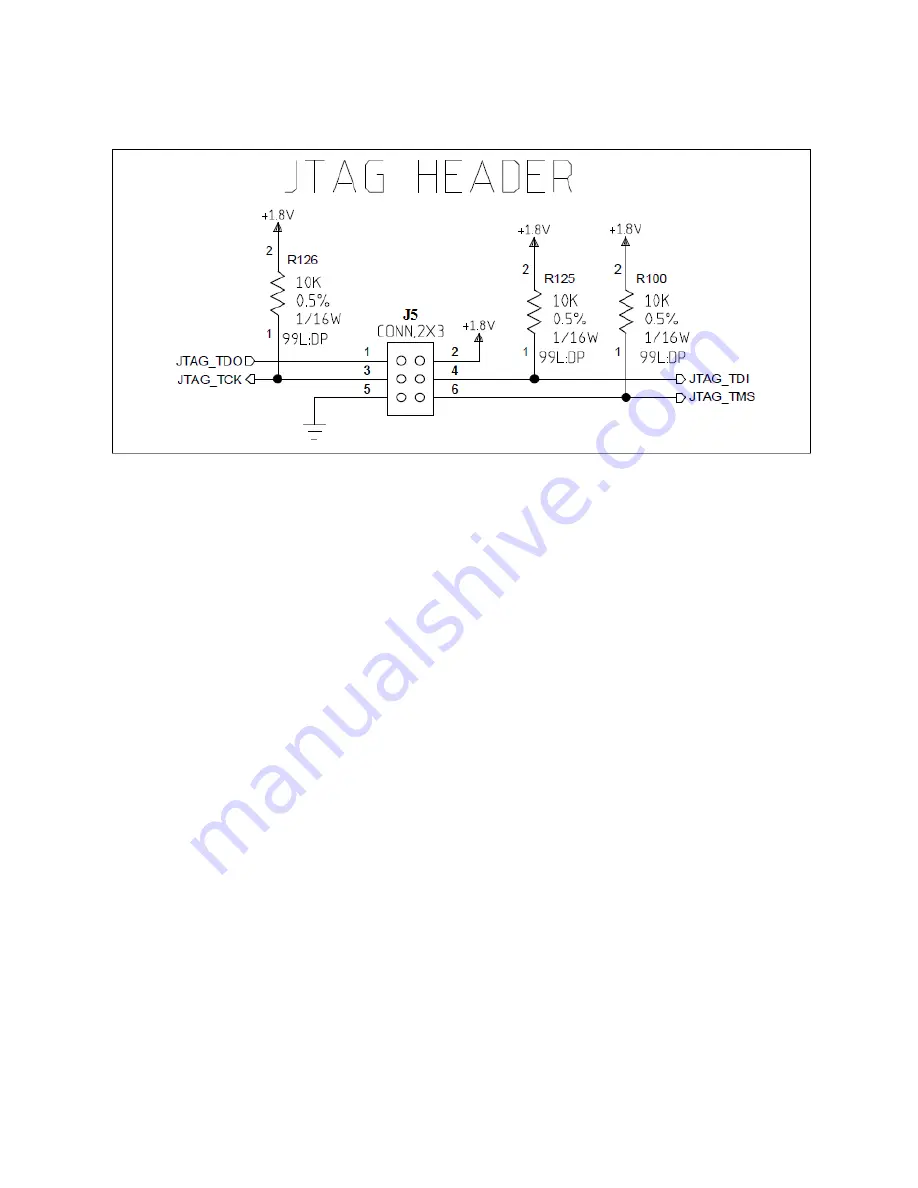
The following figure shows the JTAG header's pinnout.
Figure 2: Pinnout of JTAG header
Page 1: ...Devices in JTAG Chain2 1st Zynq PS Arm processor 2nd Zynq PL FPGA Fabric 3rd LCMXO2 640 CPLD2 Number of JTAG Instruction Registers Zynq PS 4 Zynq PL 6 CPLD 8 1 NOTE that the JTAG pins are ESD sensitive Additionally they may be damaged if overvoltage above 1 8V Be sure to attach the VREF pin of the JTAG programmer properly Do not force the JTAG programmer to use any voltage other than 1 8V on its I...
Page 2: ... JTAG on the myRIO 1950 be sure that header J5 is populated If it is not then populate this header with a through hole 2x3 0 1 spaced standard header Note that Pin 1 is labeled with a 1 and pin 6 is labeled with a 6 Figure 1 JTAG Header Location ...
Page 3: ...The following figure shows the JTAG header s pinnout Figure 2 Pinnout of JTAG header ...
Page 4: ...uction register length of each of the devices in the chain Here is an example of such configuration from the Xilinx XMD software IR stands for instruction register Figure 3 Example JTAG configuration 3 Configure the JTAG operating frequency to 10Mhz or slower 4 After you configure these settings you should be able to communicate with any device in the JTAG chain DO NOT USE SOFTWARE TO RECONFIGURE ...
Page 5: ...n LOC F20 IOSTANDARD LVCMOS33 DRIVE 8 SLEW SLOW output NET aAiSpiClk LOC F19 IOSTANDARD LVCMOS33 DRIVE 8 SLEW SLOW output NET aAiSpiMosi LOC G18 IOSTANDARD LVCMOS33 DRIVE 8 SLEW SLOW output NET aAiSpiMiso LOC G17 IOSTANDARD LVCMOS33 DRIVE 8 SLEW SLOW input DACs DAC7562SDSC There are 2 Dac devices selectable with the Cs 0 and Cs 1 pins Note how this logic is inverted logic from a typical SPI port N...
Page 6: ...output NET aMxpBdio8 LOC W16 IOSTANDARD LVCMOS33 DRIVE 8 SLEW SLOW input output NET aMxpBdio9 LOC V16 IOSTANDARD LVCMOS33 DRIVE 8 SLEW SLOW input output NET aMxpBdio10 LOC R17 IOSTANDARD LVCMOS33 DRIVE 8 SLEW SLOW input output NET aMxpBdio11 LOC R16 IOSTANDARD LVCMOS33 DRIVE 8 SLEW SLOW input output NET aMxpBdio12 LOC R18 IOSTANDARD LVCMOS33 DRIVE 8 SLEW SLOW input output NET aMxpBdio13 LOC T17 IO...
Page 7: ... OUT 20 ns AFTER Clk40 Accelerometer I2c Parameter Special Pinnout instructions 1 In your FPGA drive aDriveLow0 aDriveLow1 and aDriveLow3 to a 0 These are used to control some proprietary circuitry If these are not driven low then the analog input s input impedance will be different than specified in the myRIO user manual 2 Configure RESERVED pins as inputs DO NOT DRIVE THESE PINS YOU MAY DAMAGE Y...