background image

Chapter 1

User Interface

©

 National Instruments Corporation

1-13

NI Ultiboard User Manual

Setting Preferences 

This section explains general procedures for setting preferences. The 
following sections describe details of setting specific options. 

Complete the following steps to set your user preferences: 

1.

Choose 

Options»Global Preferences

. The 

Preferences

 dialog box 

appears, offering you the following tabs: 

General Tab


Paths Tab


Colors Tab


PCB Design Tab


Dimensions Tab


3D Options Tab


2.

Select the desired tab. 

3.

Set the desired customization options. The specific options and 
settings available in the tabs are described in the following sections. 

4.

Click 

OK

 to save your changes. 

General Tab 

Complete the following steps to change workspace options: 

1.

Choose 

Options»Global Preferences

 and select the 

General 

tab.  

2.

Set the 

Fullscreen mode

View

Crosshair

 and 

Mouse wheel 

behavior

 settings as desired. 

3.

Set the following as desired: 

Auto save settings

—Enable to have changes automatically saved 

(at the specified 

Time interval

). 

Minimum control point size

—The size of the contol points on 

vertices and other objects. 

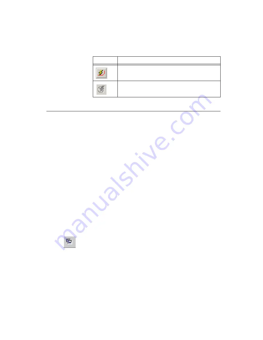
Start/Resume Autorouting 

button. Starts automatically 

placing traces.  

Stop/Pause Autorouter

 button.  

Button

Description

Summary of Contents for Graphical User Interface Ultiboard

Page 1: ...NI Ultiboard TM User Manual NI Ultiboard User Manual May 2008 374488C 01...

Page 2: ...ebanon 961 0 1 33 28 28 Malaysia 1800 887710 Mexico 01 800 010 0793 Netherlands 31 0 348 433 466 New Zealand 0800 553 322 Norway 47 0 66 90 76 60 Poland 48 22 3390150 Portugal 351 210 311 210 Russia 7...

Page 3: ...on retrieval system or translating in whole or in part without the prior written consent of National Instruments Corporation National Instruments respects the intellectual property of others and we as...

Page 4: ...ART OF THE USER OR APPLICATIONS DESIGNER ADVERSE FACTORS SUCH AS THESE ARE HEREAFTER COLLECTIVELY TERMED SYSTEM FAILURES ANY APPLICATION WHERE A SYSTEM FAILURE WOULD CREATE A RISK OF HARM TO PROPERTY...

Page 5: ...ry data loss or a system crash bold Bold text denotes items that you must select or click in the software such as menu items and dialog box options Bold text also denotes parameter names italic Italic...

Page 6: ...eneral Tab 1 13 Paths Tab 1 14 Colors Tab 1 15 PCB Design Tab 1 15 Dimensions Tab 1 18 3D Options Tab 1 19 Setting PCB Properties 1 20 Attributes Tab 1 20 Grid Units Tab 1 20 Copper Layers Tab 1 21 Pa...

Page 7: ...of Pop up Menus 1 49 Chapter 2 Beginning a Design About Designs and Projects 2 1 Creating a Project 2 1 Creating a Design 2 2 Creating a Design from a Netlist File 2 2 Working with Projects 2 4 Openi...

Page 8: ...19 Part Group Settings 3 19 Differential Pair Settings 3 20 Chapter 4 Working with Parts Placing Parts 4 1 Dragging Parts from Outside the Board Outline 4 1 Using the Parts Tab in the Spreadsheet View...

Page 9: ...Properties 4 31 Viewing and Editing SMT Pin Properties 4 33 Searching For and Replacing Parts 4 34 Searching for Parts in Open Designs 4 34 Locating a Part in a Design 4 34 Replacing Parts 4 35 Cross...

Page 10: ...pper Properties 5 13 Working with Vias 5 15 Placing Vias 5 15 Viewing and Editing Via Properties 5 16 Placing SMD Fanouts 5 18 Working with Nets 5 19 Using the Nets Tab 5 19 Using the Netlist Editor 5...

Page 11: ...re Placing Parts 7 2 Understanding How the Autoplacer Works 7 2 Running the Autoplacer 7 3 Controlling the Autoplacer 7 3 Strategies to Achieve Better Part Placement 7 5 Autorouting 7 6 Understanding...

Page 12: ...ng Gerber Properties 8 10 Setting DXF Properties 8 11 Setting NC Drill Properties 8 11 Working with SVG Properties 8 11 Working with other Properties 8 12 Exporting the Desired File 8 14 Printing your...

Page 13: ...ve As A 2 File Save All A 2 File Close A 2 File Close Project A 2 File Close All A 2 File Import A 2 File Export A 2 File Save Technology A 2 File Load Technology A 2 File Print Setup A 3 File Print P...

Page 14: ...ar A 9 View Density Bars A 9 View Birds Eye A 9 View Design Toolbox A 9 View Spreadsheet View A 9 View 3D Preview A 9 View Toolbars A 9 Place Menu A 10 Place From Database A 10 Place Line A 10 Place S...

Page 15: ...Design Remove Unused Vias A 16 Design Group Replica Place A 16 Design Copy Route A 16 Design Highlight Selected Net A 16 Tools Menu A 17 Tools Board Wizard A 17 Tools Part Wizard A 17 Tools Database D...

Page 16: ...se All A 21 Window Cascade A 21 Window Tile Horizontal A 21 Window Tile Vertical A 21 Window Windows A 21 Window open designs A 21 Help Menu A 21 Help Ultiboard Help A 21 Help Release Notes A 21 Help...

Page 17: ...ssists you in carrying out the major steps in the circuit design flow Ultiboard is used to design printed circuit boards perform certain basic mechanical CAD operations and prepare them for manufactur...

Page 18: ...mples folder Save File button Saves the active design to its current name and directory Refer to the Saving and Closing section of Chapter 2 Beginning a Design for more information Print button Displa...

Page 19: ...Screen button Adjusts the size of the workspace so it displays the entire design Refer to the Using the Full Screen section of of Chapter 2 Beginning a Design for more information Zoom In button Zoom...

Page 20: ...ard button Launches the Board Wizard Refer to the Using the Board Wizard section of Chapter 3 Setting Up a Design for more information Part Wizard button Starts the Part Wizard Refer to the Using the...

Page 21: ...r Plane button Places a powerplane on the design Refer to the Placing Powerplanes section of Chapter 5 Working with Traces and Copper for more information Design Rule Check button Runs the Design Rule...

Page 22: ...n of vias Enable Selecting Pads button Use to allow or prevent selection of pads Enable Selecting SMD Pads button Use to allow or prevent selection of Surface Mount Device pads Enable Selecting Attrib...

Page 23: ...utton Activates In Place Edit for placed PCB parts Refer to the Editing a Placed Part In Place Edit section of Chapter 4 Working with Parts for more information Toggle In Place Edit Text or Attribute...

Page 24: ...dges of the selected parts Align Bottom button Aligns the bottom edges of the selected parts Align Center Horizontal button Shifts the selected elements horizontally so their centers are aligned Align...

Page 25: ...f the screen and places it on the system clipboard Select button De activates any selected mode for example for placing traces and allows you to select an element on the board Place Line button Places...

Page 26: ...on the design Refer to the Placing Shapes and Graphics section of Chapter 4 Working with Parts for more information Place Copper Area button Places a polygon copper area on the design Refer to the Pla...

Page 27: ...nformation Place a Vertical Dimension button Places a vertically oriented dimension between two selected points Refer to the Working with Dimensions section of Chapter 4 Working with Parts for more in...

Page 28: ...or more information Remove Copper Islands button Removes copper islands Refer to the Placing Copper Areas section of Chapter 5 Working with Traces and Copper for more information Button Description Bo...

Page 29: ...t the desired customization options The specific options and settings available in the tabs are described in the following sections 4 Click OK to save your changes General Tab Complete the following s...

Page 30: ...can point Ultiboard to a new location to find for example database files You can also use this dialog box to create and specify user settings files that contain individuals preferences for all options...

Page 31: ...r OK To create a color scheme click New scheme and provide a scheme name The element colors remain at the value they had in the most recently loaded scheme Modify the element colors as described above...

Page 32: ...ea Units Select unit of measurement from drop down list Jumpers Enter the default pin diameter for jumpers Testpoints Enter the default pin diameter for testpoints 7 In the Action on DRC error area se...

Page 33: ...able to have the next trace begin from the finish point of the previous trace when placing a Follow me trace If this is not selected you must click to start a new trace Refer to the Placing a Trace Fo...

Page 34: ...ion of Chapter 4 Working with Parts for information about placing dimensions Complete the following steps to define the default dimension characteristics 1 Choose Options Global Preferences The Prefer...

Page 35: ...are not affected To apply your changes and close the dialog box click OK 3D Options Tab Complete the following steps to set 3D viewer options 1 Choose Options Global Preferences and select the 3D Opt...

Page 36: ...r to the Attributes section of Chapter 4 Working with Parts for information about adding attributes Grid Units Tab Use the Grid Units tab of the PCB Properties dialog box to control Ultiboard grids an...

Page 37: ...oices will affect the cost of the board and should be confirmed with the board manufacturer This tab also allows you to set the default clearance for the board the distance from the edge of the board...

Page 38: ...er for which you wish to assign routing properties and click Properties to display the Copper Layer Properties dialog box Enable the Routable checkbox to allow routing on the selected layer In the Tra...

Page 39: ...e that the annular ring will never go beyond those bounds Complete the following to enter an annular ring setting 1 Click the button beside the desired field Top Inner or Bottom in the Pad Vias tab Th...

Page 40: ...be added to the pad In the case of a circular pad this amount is added to the radius In the case of a rectangular or square pad the amount will be added to the width and length General Layers Tab Use...

Page 41: ...imum trace neck length Clearance Settings Set clearance to traces pads vias and copper areas For all of these clearances to be active and display in the Spreadsheet View the Use multiple clearances ch...

Page 42: ...be made Complete the following steps to assign shortcut numbers to layers 1 Click on the Favorite layers tab 2 Select the desired layer from the drop down list beside each layer number For example yo...

Page 43: ...ontrolling major parts of Ultiboard s functionality To toggle it on or off select View Design Toolbox The Design Toolbox is made up of two tabs The Projects tab lets you view the projects that are cur...

Page 44: ...they have been disabled in the Layers tab of the Design Toolbox In the example in the figure below the green rectangle that was drawn encloses the four ICs in the middle of the Birds Eye View and the...

Page 45: ...ppear in all tabs Button Description Export to Textfile button Displays a standard Windows Save dialog where you save the selection as a textfile Export to CSV File button Displays a standard Windows...

Page 46: ...n Zooms in on the selected part Refer to the Using the Parts Tab for Other Functions section of Chapter 4 Working with Parts for more information Lock the Selected Part button Locks the selected unloc...

Page 47: ...arning types from the filter All errors and warnings will now show in the DRC tab Start Filter Manager Click to start the Filter Manager Refer to the Filter Manager section for more information Filter...

Page 48: ...ter Manager select the error type and click Remove Filter To remove all error types click Remove All Spreadsheet View Results Tab The Results tab displays the results of searching for elements in the...

Page 49: ...green Orange indicates the part has been locked RefDes The part s Reference Designator unique identifier Value The part s value for example 150 pF for a capacitor Shape The physical footprint of the p...

Page 50: ...a Design for more information Part Group The group in which the part is placed You can select No Group or an existing group from the drop down list Parts groups are created in the Group Editor Refer t...

Page 51: ...e colored circle indicates whether the copper for the net has been routed that is placed on the board outline bright green or is awaiting placement dark green Orange indicates the copper for the net h...

Page 52: ...copper in a net Not applicable N A if Topology is set to Shortest Trace Clearance This is the minimum spacing allowed between the parts in the group and any trace You can enter a value here or use th...

Page 53: ...n Shield Net Use the drop down list to select the net to use to shield this net This feature is not available in all versions of Ultiboard Shield Width Width of the net s shield This feature is not av...

Page 54: ...the Working with the Group Editor of Chapter 3 Setting Up a Design section for more information Min Width The minimum width to which a trace in the group will be laid during routing You can enter a va...

Page 55: ...and Pin Number For example U1 P1 is pin number one of the device with RefDes U1 Pad Shape The shape of the pad as set in the SMT Pin Properties dialog box Refer to the Viewing and Editing SMT Pin Pro...

Page 56: ...here the trace attaches to the pin as set in the SMT Pin Properties dialog box You can also enter the value here Refer to the Viewing and Editing SMT Pin Properties section of Chapter 4 Working with P...

Page 57: ...g box Refer to the Viewing and Editing Through Hole Pin Properties section of Chapter 4 Working with Parts for more information Pad Diameter The diameter of the pad as set in the Through Hole Pin Prop...

Page 58: ...Via Properties section of Chapter 5 Working with Traces and Copper for more information Drill Diameter The diameter of the drill hole in the via as set in the Via Properties dialog box Refer to the V...

Page 59: ...the net to which the copper area is connected Trace Clearance The minimum clearance permitted between the copper area and traces as set in the Copper Area Properties dialog box Refer to the Viewing an...

Page 60: ...Working with Traces and Copper for more information Locked Yes means that the Keep in out area cannot be moved or edited No means that the Keep in out area can be moved Layers To Apply Double click t...

Page 61: ...Assign a height z axis value to theKeep in out Can be entered directly or in the Keep in Keep out Properties dialog box Refer to the Working with Keep in Keep out Areas section of Chapter 5 Working w...

Page 62: ...be docked in various positions and orientations The contents of the toolbars may be customized New toolbars can be created The menu system is fully customizable including all pop up menus for the var...

Page 63: ...owing click on the Toolbars tab and click in the checkbox beside the desired toolbar to make it visible 4 Click Close when customizations are complete To remove a command from a menu or toolbar right...

Page 64: ...how text labels Select this checkbox to show the text labels for example Save in the toolbar along with the command s icon 4 Click Close when customizations are complete Keyboard Tab The Keyboard tab...

Page 65: ...p up Menus To customize the appearance of toolbar buttons and menu items a pop up menu is available when the Customize dialog box is open Complete the following steps to display the pop up 1 Be sure y...

Page 66: ...plete the following steps to create a new project file 1 Choose File New Project The New Project dialog box appears 2 Type the project name in the Project name field 3 From the Design type drop down l...

Page 67: ...dialog box disappears and a blank design with the name that you specified is opened The Projects tab shows that the new design is a part of the project file that you specified Creating a Design from...

Page 68: ...0000 routing_layer settings_locked 0 net_group The following is an example of component information from a netlist file components instance 7SEG8DIP10A U1 device SEVEN_SEG_DECIMAL_COM_A_BLUE value SEV...

Page 69: ...example Add New Net VCC and click OK A board outline is placed on the workspace with the parts ready to be placed Working with Projects Designs and projects appear in the Projects tab of the Design To...

Page 70: ...and any other software select 3 Select a file from the list displayed and click Open The file opens along with its associated project If you open an Ultiboard project file you see the designs within t...

Page 71: ...save a design s technology specifications 1 Have the desired design open in Ultiboard 2 Select File Save Technology The Technology File Settings dialog box appears 3 Select the technology parameters y...

Page 72: ...longing to the trace you want to select 2 Choose Edit Select Entire Trace The entire trace is then selected To unselect one element select another element or click outside of the board outline To unse...

Page 73: ...ncel the place mode and return to select mode 1 Right click Or Press ESC Or Choose Place Select Searching for Design Elements To find out if an element exists in an open project you can search for it...

Page 74: ...the Results tab Or Right click on the desired element and select Go to from the pop up menu that appears The element is selected and shown in the workspace To clear the information in the Results tab...

Page 75: ...n display to the multi screen display 1 Locate the Full Screen Close button It will be floating over the design 2 Click the Full Screen Close button to return to the multi pane display Magnifying and...

Page 76: ...cluding the limitations of the computer monitor being used although it does not affect the design Complete the following to clean up the design removing any extraneous images that should not be there...

Page 77: ...d buried vias to a normal feed through design after the board has been completed Your decisions are also important in terms of manufacturing cost A 6 layer board with blind and buried vias will cost s...

Page 78: ...internal Micro via A via that is less than 5 mils in diameter that connects a maximum of two build up layers only The lamination sequence used determines the acceptable layer combinations for placing...

Page 79: ...he Layers tab in the Design Toolbox The tab appears as shown in the figure below Layers with a check mark are displayed on the workspace Layers with a check mark in a grey box are displayed in the wor...

Page 80: ...ore information The layer highlighted in red is the active layer The one which any functions you choose will affect Before you can work on a particular layer you must ensure that layer is active Depen...

Page 81: ...the drawing tools Refer to the Using the Drawing Tools to Create a Board Outline section for more information Import a DXF file Refer to the Importing a DXF File section for more information Place a...

Page 82: ...ing layer radio button Merges DXF file layers into the layer chosen from the drop down list 5 In the Units box set the following as desired Interpret units in file as radio button Select a unit of mea...

Page 83: ...ias checkboxes to use these in your design As you make changes to the layer settings the information window shows the acceptable layer combinations for blind and buried vias In this window select the...

Page 84: ...clearance or trying to place a part so that a pad is put within a clearance for example results in a design rule error 5 Click Finish The board outline is placed on your design Setting the Board s Re...

Page 85: ...rdinates and the desired units of measure 3 Optionally select Snap to grid to have the reference point snap to the closest grid on the workspace Note If you do not have a part selected and you press t...

Page 86: ...area on the design which will be indicated with a red circle as shown in the example below Depending on what you are doing on the board you may see the following kinds of errors if you keep the DRC ta...

Page 87: ...netname The given net was too close to another net You can set up whether the design rule check runs in real time and define the actions to be taken when Ultiboard encounters a design rule error such...

Page 88: ...ars 4 Enter the desired name and click OK The Change group settings dialog box appears 5 Change the settings in the Group Settings area as desired Note Refer to the Change Group Settings dialog box an...

Page 89: ...ck the Properties button to display the Change group settings dialog box 6 Make the required changes in the Group Settings area and click OK Note Refer to the Change Group Settings dialog box and Net...

Page 90: ...ple below 8 Click checkboxes beside the desired parts in the Assign Parts list and click Apply to add them to the group Note You cannot assign a part to more than one group Therefore parts that are al...

Page 91: ...alog box and Net Group Settings sections for more information Complete the following steps to delete a group 1 Select Tools Group Editor to display the Edit Groups dialog box 2 Select the Part Groups...

Page 92: ...gn Nets list 8 Click OK to close the Edit Groups dialog box Complete the following steps to edit a bus group 1 Select Tools Group Editor to display the Edit Groups dialog box 2 Select the Bus Groups t...

Page 93: ...box appears 4 Enter the desired name and click OK The Change group settings dialog box appears 5 Change the settings in the Group Settings area as desired Note Refer to the Change Group Settings dialo...

Page 94: ...d click the Properties button to display the Change group settings dialog box 6 Make the required changes in the Group Settings area and click OK Note Refer to the Change Group Settings dialog box and...

Page 95: ...that you set to a 5 mils clearance moves to 5 mils or less from one of the other traces with the 5 mils clearance setting a DRC error occurs Note Set individual trace clearances in the Nets tab of th...

Page 96: ...the descriptions Do this by dragging the dialog s lower right corner Differential Pair Settings For differential pairs the following Group Settings are available Length Constraints Space Constraints F...

Page 97: ...utline Refer to the Dragging Parts from Outside the Board Outline section for more information by using the Spreadsheet View Refer to the Using the Parts Tab in the Spreadsheet View section for more i...

Page 98: ...accidentally moved and place parts on the board It also contains functions to help you find parts on the board and preview a selected part The dark green indicator 1 shows that the part has not been...

Page 99: ...ard The part can then be adjusted or moved further into position as needed Refer to the Tools to Assist Part Placement section for more information about moving parts and adjusting their placement Com...

Page 100: ...o unlock the selected locked parts Complete the following steps to find a part in the design 1 Click the part in the list 2 Click the Find and Select the Part button The view zooms in on the part whic...

Page 101: ...connections that can overlap parts and other ratsnest lines In Ultiboard ratsnests are represented by colored lines although they can be dimmed so that they appear gray They appear by default exist o...

Page 102: ...ection of the force vector and trying to minimize the force vector length you are moving the part to a location that results in the shortest possible combination of ratsnest lines Note Force vectors a...

Page 103: ...If connections are lost they can be restored by putting the part s pad back on the trace to which it belongs with the same net name Rubber Banding When you move a part that has connected traces its c...

Page 104: ...for the selected part 1 In the Swapping box Pin Select Yes No or Use Group Settings from the drop down list Gate Select Internal Gates only to permit swapping of gates between gates within the same p...

Page 105: ...ore of the whole part You can also press the F9 key Zoom Window button Click or press F6 and then drag a rectangle around the portion of the part you want to enlarge The area inside the rectangle enla...

Page 106: ...easurement where you want the guide placed shown in 1 in the figure below Guides and dotted lines appear as shown in 2 3 below To move a guide click on it in the ruler bar and drag it to a new locatio...

Page 107: ...ounter clockwise Angle Rotates the part at an angle that you define Swap Layer Swaps the selected part to the mirror layer for example from Silkscreen Top to Silkscreen Bottom Aligning Shapes and Part...

Page 108: ...y Space Down Plus Increases vertical space between two or more objects Space Down Min Decreases vertical space between two or more objects Placing a Group Array Box A group array box is used to place...

Page 109: ...anual 5 Begin selecting and dragging parts As they are placed the parts snap to the array Place the part in the top left cell The other parts will be placed at the same relative position in the other...

Page 110: ...Chapter 3 Setting Up a Design for information about group creation Complete the following steps to replicate the positioning of a group of parts 1 Select Design Group Replica Place to display the Sel...

Page 111: ...d parts is also removed If you chose No the copper remains in place Viewing and Editing Properties Once a shape or a part has been created its properties can be viewed and edited This section explains...

Page 112: ...the Value field Choose the attribute s Visibility by enabling the desired option Visible attributes are previewed in the Alignment area of the dialog box Use the Alignment area to set the attribute s...

Page 113: ...operties are reflected in the Preview area The Enable 3D for this object checkbox must be selected for the part to appear in the 3D view Tip Enable the Automatic preview update checkbox to have the pr...

Page 114: ...h of the following field labels and choose a color from the dialog box that appears Part The color used when the part s face is viewed at right angles to a line from the viewer to the part Backlight T...

Page 115: ...he following steps to view an attribute s properties 1 Select the attribute for example the Reference Designator 2 Select Edit Properties The Attribute Properties dialog box appears containing three t...

Page 116: ...t editing properties in the Attributes tab Depending on the shape graphic selected the General tab lets you change the width and the clearance of the selected element and define the units of measureme...

Page 117: ...e Plated in the Drill Option area if you wish the hole to be plated 5 Click OK The dialog closes and the hole is placed on the cursor 6 Move the cursor to the desired location and click to place it on...

Page 118: ...nts that define the circle s diameter Place Shape Pie Left click to define two points that define the diameter of the pie then move the pointer back and forth to define whether the shape looks like a...

Page 119: ...he design The pointer has the first prong of the jumper attached 4 Click to drop the first prong of the jumper then move the pointer to where the second prong should be placed 5 Click to drop the seco...

Page 120: ...Hole Technology or Surface Mount Technology Units Units of measurement Working with Test Points Placing Test Points Default test point pin settings are defined in the PCB Design tab of the Preferences...

Page 121: ...se the Attributes tab Refer to the Attributes section for more information Working with Dimensions Placing Dimensions Dimensions can be placed on a silkscreen top or bottom layer To set dimension para...

Page 122: ...Position Line and Dimensions To edit a dimensions s properties select the dimension and select Edit Properties To edit a dimension s attributes use the Attributes tab Refer to the Attributes section f...

Page 123: ...t The radio buttons in this box set the dimension s alignment Auto Left Center Right Position The radio buttons in this box set the position of the dimension Outside Inside Above Over Below Orientatio...

Page 124: ...en enlarged beyond the borders of the Preview area scroll bars appear that you can move in the usual manner to locate the desired section of a part 4 Click OK The Get a part from the Database dialog b...

Page 125: ...Edit In Place Part Edit An editing window opens showing the selected part The window also shows the surrounding area of the board and the other parts in a dimmed view which cannot be edited In the ex...

Page 126: ...ointer Click on the part to place it 5 When finished choose Edit In Place Part Edit again to end the In Place Edit function The part appears with its changes Note You can save your edited part in the...

Page 127: ...ck on the point to be removed 2 Choose Edit Vertex Remove Vertex The vertex is removed and the vertices on either side are joined by a straight line Complete the following to change the size of a desi...

Page 128: ...space Shape box Choose options to control the shape of the through hole pin Shape settings can be set differently for each layer if desired Pad Size box Choose the appropriate option and where necessa...

Page 129: ...information To edit an SMT pin s display style use the following options in the General tab X The x axis coordinate Y The y axis coordinate Net The net this SMT pin is on read only Angle degrees The a...

Page 130: ...alue or by all variables Complete the following steps to find out if a part exists in the open designs 1 Choose Edit Find The Find dialog box opens 2 Enter your search criteria from the selection belo...

Page 131: ...with the part you chose from the database Cross probing Cross probing is the ability to highlight a selected part or group of parts in Multisim Complete the following steps to perform cross probing 1...

Page 132: ...for the new part The name must be unique 8 Click OK The Insert the selected Item s into the database dialog box disappears but the edit mode window stays visible The part can be placed from the datab...

Page 133: ...The following Package Dimension choices appear Units Select the unit of measure from the drop down list X The x dimension of the part displayed on the preview Y The y dimension of the part displayed o...

Page 134: ...nd on whether you selected THT or SMT in step 1 of the wizard If you chose THT the following options appear Units The unit of measure for the settings Drill Hole Diameter Diameter of the through hole...

Page 135: ...splayed in the lower right preview area Rounded Corner Enable to make pads with rounded corners and enter the desired Rounded rectangle X Rounded rectangle Y and Corner Radius settings The changes are...

Page 136: ...on of Pad Numbering Displays the available options for the selected package type Start Number Offset Offsets the starting position of the pad numbers 9 Make the desired Pad Numbering settings and clic...

Page 137: ...eir sub categories The Database panel contains the following buttons Refer to the Working with Database Categories section for more information Button Description New button Creates a new database cat...

Page 138: ...Zoom In button Click to zoom in on the part for more detail You can also press the F8 key Zoom Out button Click to zoom out Shows less detail and more of the whole part You can also press the F9 key Z...

Page 139: ...e Manager just as you would in similar Windows applications click the plus to expand a category or subcategory and click the minus to collapse it While there are default categories and sub categories...

Page 140: ...lect the sub category to be renamed 2 Click the Rename button above the Database panel The name of the sub category is highlighted 3 Change the name as desired Complete the following steps to move a d...

Page 141: ...ct all parts click the Select All Items button or press Ctrl A To deselect all parts click the Unselect All Items button 5 To rename a part highlight it and click the Rename button The part name must...

Page 142: ...uter Complete the following steps to merge databases 1 Select Tools Database Merge Database The Database Merge dialog box appears 2 Click on Select a Component Database Name in the Source Database are...

Page 143: ...atabase is loaded when you install Ultiboard Complete the following steps to update your databases to Ultiboard 10 format 1 Select Tools Database Convert Database The Select Type dialog box appears 2...

Page 144: ...Manual 4 48 ni com 7 Select one of the following options Auto Rename Imports and automatically renames the duplicate parts Overwrite Replaces the Ultiboard 10 parts with your old parts Ignore Does no...

Page 145: ...ollow me router This method allows you to select the next pad or via to be connected by having Ultiboard follow your mouse movement as it places a trace Ultiboard routes the resulting trace around mos...

Page 146: ...of 10 mil Clearances are measured from the outside edge of an object a 10 mil trace with a 5 mil clearance would measure 20 mil across from edge to edge 5 mil clearance on one side the 10 mil trace a...

Page 147: ...pop up that appears 3 Continue placing the trace and left clicking to anchor trace segments The width of the trace segments either increases or decreases by 10 of the width of the previous trace segm...

Page 148: ...used to connect more than two pads at a time Complete the following steps to place a Connection Machine trace with default routing 1 Choose a copper layer 2 Choose Place Connection Machine 3 Click a...

Page 149: ...empt to change to a net width that is too big DRC errors appear the trace width will not change Placing a Bus Use to connect multiple traces between multi pinned devices such as ICs The procedure belo...

Page 150: ...ficulty you will have routing traces through that section of the board and the more copper is used in that area When placing parts you should strive to achieve relatively equal density distributions t...

Page 151: ...efine the polygon ending with the starting point Viewing and Editing Keep in Keep out Properties To display the Keep in Keep out properties dialog box select the desired keep in out and select Edit Pr...

Page 152: ...roup Displays the Select Groups dialog box where you select the part groups to which you wish to apply the Keep in out area 5 Click OK in the Keep in Keep out Properties dialog box If no Advanced opti...

Page 153: ...below Note The selected traces must be between two objects that is two pins two traces initial spacing between traces must not be equal traces must belong to a net in the same layer Rubber banding do...

Page 154: ...anes Splitting Copper Converting a Copper Shape to an Area Deleting All Copper Adding and Removing Teardrops Placing Copper Areas Use the Place Copper Area command to define copper polygons Complete t...

Page 155: ...Click OK The Choose Net and Layer for Powerplane dialog box disappears and the powerplane is placed on the layer that you specified Splitting Copper The Polygon Splitter is used to split copper areas...

Page 156: ...shape to an area 1 Select a copper shape in your workspace The figure below shows a coppers shape green that straddles two pins and traces 2 Select Design Shape to Area The copper is cut out to avoid...

Page 157: ...tandard vias checkboxes check as desired 5 In the On DRC error box select the desired radio button Choices are Do not create teardrop Ask for confirmation Create teardrop 6 Enable or disable the Ignor...

Page 158: ...the following in the Points box X1 The X coordinate of the trace s starting point X2 The X coordinate of the trace s ending point Y1 The Y coordinate of the trace s starting point Y2 The Y coordinate...

Page 159: ...nnected to the copper area 4 If you wish to connect the copper area to a net enable Connected to Net and select the desired net from the list Working with Vias This section contains the following topi...

Page 160: ...In the Measurements box set the following as desired X Y The X and Y coordinates of the via Net The net the via is connected to read only Angle degrees Leave at 0 00 Board side Select either Top or Bo...

Page 161: ...ring autorouting 3 In the Solder Mask box select the following as desired Top checkbox Enable to place a solder mask on the top of the PCB Bottom checkbox Enable to place a solder mask on the bottom o...

Page 162: ...ed part only 4 In the Fanout Via Configuration box enter the following as desired Via Drill Diameter The diameter of the placed vias holes Via Pad Diameter The diameter of the placed vias pads Via Spa...

Page 163: ...Net Shielding Nets Net Bridges Copying a Copper Route Using the Nets Tab The Nets tab buttons in the Spreadsheet View allow you to preview a net in relation to the board find a net highlight a select...

Page 164: ...cked net or to unlock a locked net Complete the following steps to remove the copper of a selected net 1 Click the net in the list 2 Click Remove Copper You are prompted to confirm the removal 3 Click...

Page 165: ...ratsnests Adding a Net Complete the following steps to add a net 1 Select Tools Netlist Editor and click the Pins tab 2 Click New The Add Net dialog box displays 3 Enter a name and click OK The new ne...

Page 166: ...l 5 22 ni com The remainder of this section uses the example shown in the figure below The parts shown are not connected any net 3 Click the Add pins button and click the desired pin in the workspace...

Page 167: ...ck Add The dialog box closes and the Net edit dialog box shows the added pins in the list of pads for the displayed net 4 Click OK in the Net edit dialog box The dialog box closes and the net informat...

Page 168: ...stance possible will be maintained The order for the connection is not considered Refer to the figure below for an example Daisy chain The connection between pins is based on the order in which the pi...

Page 169: ...w net name appears in the Net drop down list in the Net edit dialog box and in the Nets tab in the Spreadsheet View Deleting a Net Complete the following steps to delete a net 1 Select Tools Netlist E...

Page 170: ...ace width Default trace width Maximum trace width and Trace clearance or choose Use Group Settings from the drop down lists 4 Click OK to save changes Setting High Speed Parameters Complete the follow...

Page 171: ...is not required 5 In the Net Shielding area Select which Net is used for the shield Width becomes active change as desired Note Shields are copper that is placed around a selected net to act as a buf...

Page 172: ...ab of the Spreadsheet View Tip You can change the highlight color from the Color Element drop down list in the Colors tab of the Preferences dialog box Shielding Nets Complete the following steps to s...

Page 173: ...o use for the shield 6 In the On DRC Error area select the action to take when a DRC error occurs 7 In the On Other Failures area select the action to take when other errors occur 8 In the Nets area s...

Page 174: ...art button in the Parts area select Net bridge and click OK The Net Bridge Edit Layer displays on your workspace 3 Select Place Net Bridge Pins to display the Place Net Bridge Pin dialog box 4 Enter t...

Page 175: ...tional Instruments Corporation 5 31 NI Ultiboard User Manual 7 Close the Net Bridge Edit Layer and when prompted Click Save 8 The following dialog box appears Enter the name for the new netbridge Netb...

Page 176: ...ialog box appears 2 Click Select Net Bridge From Database The Get a part from the database dialog box appears 3 Select the desired net bridge in the Available Parts area and click OK You are returned...

Page 177: ...groups that have been set up using the Group Replica command Complete the following steps to copy copper routing between groups 1 Create two identical part groups Refer to the Replicating a Group sect...

Page 178: ...opper needed to route a given net The following sections document manual pin swapping manual gate swapping and automatic pin gate swapping For these functions to work the pin groups must be set up in...

Page 179: ...tes This feature allows you to swap similar gates and works for the following which are set in the Pin Gate Swapping Settings area of the Design Rules tab of the PCB Properties dialog box Internal Gat...

Page 180: ...36 ni com The following design is used in this example Complete the following steps to swap gates between parts 1 Select Design Swap Gates The workspace changes to reflect the gates 2 Select the first...

Page 181: ...ces and Copper National Instruments Corporation 5 37 NI Ultiboard User Manual 3 Click on the letter corresponding to the gate with which you want to exchange the gate you selected above The ratsnest c...

Page 182: ...Design Rules tab of the PCB properties dialog box Complete the following steps to swap pins and gates automatically after a part move 1 Move desired parts on the workspace 2 Select Design Automatic P...

Page 183: ...ime Pin Gate Swapping This feature allows you to swap pins and or gates automatically in real time as you move parts on the workspace Note For this feature to function you must allow pin gate swapping...

Page 184: ...t will therefore have no reflections even though in reality it has a finite length What actually occurs is that all of the energy that travels down the trace is absorbed and there is no energy left to...

Page 185: ...lect Tools PCB Transmission Line Calculator 2 Select Microstrip in the Type drop down list 3 In the Input Data area edit the following fields as desired Input Length Unit Select mils or millimeters Di...

Page 186: ...lculator 2 Select Embedded Microstrip in the Type drop down list 3 In the Input Data area edit the following fields as desired Input Length Unit Select mils or millimeters Dielectric Height H1 Refer t...

Page 187: ...Tools PCB Transmission Line Calculator 2 Select Centered Stripline in the Type drop down list 3 In the Input Data area edit the following fields as desired Input Length Unit Select mils or millimeters...

Page 188: ...ssion Line Calculator 2 Select Asymmetric Stripline in the Type drop down list 3 In the Input Data area edit the following fields as desired Input Length Unit Select mils or millimeters Dielectric Hei...

Page 189: ...ne Calculator 2 Select Dual Stripline in the Type drop down list 3 In the Input Data area edit the following fields as desired Input Length Unit Select mils or millimeters Trace Separation C Refer to...

Page 190: ...ity it has a finite length What actually occurs is that all of the energy that travels down the trace is absorbed and there is no energy left to reflect back Once you have calculated Zo you can use it...

Page 191: ...mpedance calculations 1 Select Tools PCB Differential Impedance Calculator 2 Select Microstrip in the Type drop down list 3 In the Input Data area edit the following fields as desired Input Length Uni...

Page 192: ...Click Close to close the PCB Differential Impedance Calculator Microstrip Differential Impedance Equations The equations used to perform the microstrip differential impedance calculations are Z0 87 s...

Page 193: ...lect mils or millimeters Dielectric Thickness H Refer to the figure below Trace Spacing S Refer to the figure below Characteristic Impedance Zo Refer to the figure below 4 Click Calculate Results of t...

Page 194: ...Impedance Calculator 2 Select Centered Stripline in the Type drop down list 3 In the Input Data area edit the following fields as desired Input Length Unit Select mils or millimeters Dielectric Thickn...

Page 195: ...log and the Results tab when you click Calculate 5 Click Close to close the PCB Differential Impedance Calculator Centered Stripline Differential Impedance Equations The equations used to perform the...

Page 196: ...self click User Defined Zo and edit the following fields as desired Input Length Unit Select mils or millimeters Dielectric Thickness H Refer to the figure below Trace Spacing S Refer to the figure be...

Page 197: ...Stripline Differential Impedance Equations The equations used to perform the asymmetric stripline differential impedance calculations are Z0 1 H 4 H1 80 ln 4 2 H T 0 67 3 1415926 0 8 W T sqrt Er Tpd 8...

Page 198: ...and autorouting functions are accessed through the Autoroute menu Autoroute Start Resume Autorouter Use to start or resume the autorouter Refer to the Running the Autorouter section for more informati...

Page 199: ...acing other parts Complete the following steps to lock any pre placed parts so they will not be moved by the autoplacer 1 Select the pre placed parts and choose Edit Lock 2 You can also lock parts in...

Page 200: ...Refer to the Controlling the Autoplacer section for information about autoplaced parameters Controlling the Autoplacer The autoplacer is controlled from the Autoplace tab of the Routing Options dialo...

Page 201: ...ths beside each other 10 indicates a strong preference for aligning parts with equal edge lengths so the autoplacer will place parts with similar lengths beside each other whenever possible 5 In the P...

Page 202: ...ttings 8 If you wish to return the values to the default settings click Default Caution The Default button sets default values for all tabs in the Routing Options dialog box Strategies to Achieve Bett...

Page 203: ...nto the smallest possible area If the autoplacer places all but one or two parts it may be faster to simply place them on the board by hand using Ultiboard s part shoving facility not available in all...

Page 204: ...nction Rip up and Retry Routing The rip up and retry router attempts to route all open connections In some cases Ultiboard can place all traces in a single pass without rerouting any traces However if...

Page 205: ...be Moved must be selected in the Via tab of the Via Properties dialog box Routing Selected Parts and Nets Complete the following to place traces on a selection of parts 1 Select the desired parts and...

Page 206: ...rocess as desired to manually place items and then continue autorouting when ready To stop autorouting select Autoroute Stop Pause Autorouter To restart select Autoroute Start Autoplacement Autoroutin...

Page 207: ...nt on each net on your design Note Testpoints may be placed either before or after autorouting the entire board Complete the following steps to automatically place test points 1 Select Place Automatic...

Page 208: ...the traces on a grid Gridless to place them off the grid or Progressive which will attempt to place the traces on a grid and then place those that remain off the grid Grid Type Select English the rou...

Page 209: ...onnections 4 In the Screen Refresh During Routing area adjust the slider as desired to set the relative number of times the screen is refreshed during routing 5 If you wish to return the values to the...

Page 210: ...Cost Factor Sets the trace transition cost factor which the router and optimizer use to control cleanup pattern recognition during multi net optimization A high trace crossing cost factor permits comp...

Page 211: ...rees Sets the maximum number of traces that can be ripped up during each rip up cycle Maximum Rip Up Depth Controls the persistence of the rip up process The higher the value you set the greater the p...

Page 212: ...Select the Optimization tab in the Routing Options dialog box 2 Edit one or both of the fields in the Optimizer area Optimizer Passes Use to set the number of optimizer passes that are automatically a...

Page 213: ...buses to route in the Defined bus groups area Click Select All to select all available buses for routing or Clear All if you wish to clear all of the checkboxes in the Defined bus groups area 3 If yo...

Page 214: ...se powerplane layers Try gridless routing The default setting for routing is grid based which is the fastest routing algorithm If this fails to achieve completion then next step should almost always b...

Page 215: ...e following steps to place text on the design 1 Choose Place Graphic Text The Text dialog box opens 2 Type the text in the Value field As you type the text appears in the preview dialog box 3 Define t...

Page 216: ...you want the text placed and click to drop the text 7 Right click to cancel the Place Graphics Text command Complete the following steps to edit text 1 Double click the text The Copper Attribute Prop...

Page 217: ...Click on the x at the top right corner of the selection frame to close it 6 Open the desired application for example MS Word and click on Paste to paste the image Placing a Comment Adding a comment p...

Page 218: ...he comment on the design 4 Type the comment in the area below the Show Comment checkbox 5 Optionally modify the information in the Color box Background Click to change the color of the placed comment...

Page 219: ...order that you specify It is easier to produce service and troubleshoot boards when parts are ordered in a logical manner Renumbering is primarily for assembly to help locate all the elements Using t...

Page 220: ...ncies between the schematic and the PCB design Backannotation can overcome these inconsistencies To backannotate Multisim reads the log file in which Ultiboard reports all the changes that are made to...

Page 221: ...e to not be mitered The default is 0 that is all traces will be mitered regardless of the minimum length of any one segment 5 To set a maximum length for the mitering enable the Maximum Length option...

Page 222: ...ng connections in the design To delete open trace ends make sure the design is open and choose Edit Copper Delete Open Trace Ends This deletes all open trace ends in the design Deleting Unused Vias No...

Page 223: ...an also export text files that contain Board Statistics Part Centroids Bill of Materials You can also create reports on Copper Amounts Test Points Layer Stackup Exporting a file begins by opening the...

Page 224: ...rt This is done through the property dialog boxes that correspond to the devices or types listed in the Export dialog box Gerber RS 274D Gerber RS 274X DXF Board Statistics Bill of Materials Parts Cen...

Page 225: ...dialog box and click properties The Drill export properties dialog box appears 2 In the Units box select either the Imperial or Metric radio button 3 Enter the following in the Digits box as required...

Page 226: ...cs on the board being exported as well as to filter the file types to be exported and to define the units of measurement in the statistics Statistics list The list at the top of the dialog displays th...

Page 227: ...of all test points on the boards and their coordinates ColumnsClick column headers in the list to sort the columns File type box Select any of TXT CSV and HTML Units box Select the unit of measurement...

Page 228: ...can define the export file s name and path If you are exporting more than one file you must define the name and path of each file 6 Select the path that defines the export file s location and type th...

Page 229: ...orientation For details refer to the Viewing Designs in 3D section of Chapter 9 Viewing Designs in 3D 3 To set up the printing of the 3D image select File Print Setup 4 To preview the printing of the...

Page 230: ...for Manufacturing Assembly NI Ultiboard User Manual 8 16 ni com If you elect to enlarge the size of your printout in the Zoom Options area each layer will be tiled onto as many pages as required to pr...

Page 231: ...3D and how to manipulate the view Some of the described features may not be available in your edition of Ultiboard Refer to the NI Circuit Design Suite Release Notes for a list of the features in your...

Page 232: ...so that you are looking at a three dimensional rendition of the top of the board on an angle You can manipulate this view to show you all points on the board top and bottom at any angle you choose Yo...

Page 233: ...he view of the edge passes release the mouse button and catch the underside of the board 3 Continue until you can see the underside of the board fully To zoom in a 3D design do one of the following Cl...

Page 234: ...t appears 3 Repeat on as many parts as desired To hide a part s height click on the part The callout with the height disappears To rotate or magnify the board select Tools View 3D Position Refer to th...

Page 235: ...terface for more information Exporting to 3D DXF Ultiboard can export a 3D DXF file for your design Complete the following steps to export a design s 3D properties 1 Select File Export to display the...

Page 236: ...rt Complete the following steps to export a design s 3D IGES properties 1 Select File Export to display the Export dialog box 2 Highlight 3D IGES and click Properties The IGES export settings dialog b...

Page 237: ...u work with mechanical CAD designs the same way that you do with PCB designs although you cannot place traces or use the Autoroute function in mechanical CAD designs Some of the described features may...

Page 238: ...gn type drop down list select Mechanical CAD 5 Indicate the file where the design is to added The drop down list shows only the open files To include this design in another project open the file so th...

Page 239: ...as with PCB properties except that mechanical CAD designs have only two grids Setting Mechanical CAD Colors 1 Choose Options Global Preferences The Preferences dialog box appears 2 Click the Colors t...

Page 240: ...s on grid Makes sure that the crosshair will always snap to grid points even when you are not placing any parts or traces normally when you are not placing parts or traces the crosshair moves gridless...

Page 241: ...he new setting Setting Paths for Mechanical CAD The Ultiboard installation puts specific files in specific locations If necessary you can point Ultiboard to a new location Complete the following steps...

Page 242: ...ds found in the File menu File New Design Creates a new design if a project is open or project if no project is open Refer to the About Designs and Projects section of Chapter 2 Beginning a Design for...

Page 243: ...rting a DXF File section of Chapter 3 Setting Up a Design for more information File Export Exports Ultiboard files for post processing Refer to the Exporting a File section of Chapter 8 Preparing for...

Page 244: ...s found in the 3D view only File Print Prints the Ultiboard design file Refer to the Printing your Design section of Chapter 8 Preparing for Manufacturing Assembly for more information File Recent Des...

Page 245: ...be R35 Edit Paste Special Paste with Net Pastes the item on the Windows Clipboard into the design with the same connectivity as the source New parts will have Reference Designators that increment fro...

Page 246: ...ent in the design Refer to the Searching for Design Elements section of Chapter 2 Beginning a Design for more information Edit Select All Use to select everything on a board no matter what layer the e...

Page 247: ...elected Enable Selecting Other Objects When enabled allows other objects on the PCB to be selected Edit Orientation Use these commands to adjust the orientation of parts as they are placed on a design...

Page 248: ...more objects Space Down Spaces three or more objects above each other evenly Space Down Plus Increases vertical space between two or more objects Space Down Min Decreases vertical space between two o...

Page 249: ...f the board Use this command when you want precise control over the workspace view View Zoom Full Use to return to the full view of the design after zooming in or out Ctrl F7 zooms out so that the ent...

Page 250: ...rmation View Design Toolbox Use to toggle the Design Toolbox on and off Refer to the Design Toolbox section of Chapter 1 User Interface for more information View Spreadsheet View Use to toggle the Spr...

Page 251: ...r 1 User Interface for more information Wizard Use to toggle the Wizard toolbar on and off Refer to the Wizard Toolbar section of Chapter 1 User Interface for more information Autoroute Use to toggle...

Page 252: ...cle Use to place a circle Pie Use to place a pie shape Rectangle Use to place a rectangle Polygon Use to place a polygon Refer to the Placing Shapes and Graphics section of Chapter 4 Working with Part...

Page 253: ...lect the desired bitmap and click to place it on the design Drag the bitmap to the desired size and click the mouse again to place it Place Graphic Text Use to place text on the design Useful for anno...

Page 254: ...ng a Placed Part In Place Edit section of Chapter 4 Working with Parts for more information Place Via Use to place a via Refer to the Working with Vias section of Chapter 5 Working with Traces and Cop...

Page 255: ...n menu Design Netlist DRC Check Use to run the design rules and netlist check utility Results are displayed in the DRC tab of the Spreadsheet View Refer to the Spreadsheet View DRC Tab section of Chap...

Page 256: ...n Swap Gates Refer to the Swapping Gates section of Chapter 5 Working with Traces and Copper for information Design Automatic Pin Gate Swap Refer to the Automatic Pin Gate Swapping section of Chapter...

Page 257: ...s that do not have any trace segments or copper areas connected to them Use this command after Edit Copper Delete Open Trace Ends to clean up the design Refer to the Deleting Unused Vias section of Ch...

Page 258: ...the Managing the Database section for more information Tools Database Add Selection to Database Use to place the selected part in the database Refer to the Adding Parts to the Database section of Chap...

Page 259: ...exactly equal and opposite a differential pair Refer to the PCB Differential Impedance Calculator section of Chapter 6 PCB Calculators for more information Tools Netlist Editor Use to remove or add ne...

Page 260: ...rt in Multisim Refer to the Cross probing section of Chapter 4 Working with Parts for more information Tools Capture Screen Area You can take a screen capture of a selected area Refer to the Capturing...

Page 261: ...Properties section of Chapter 1 User Interface for more information Options Customize User Interface Use to customize your menus toolbars and context menus Refer to the Customizing the Interface sect...

Page 262: ...o adjust two or more windows so that they sit beside each other Window Windows Displays the Windows dialog box where you can show or close the files that you currently have open Window open designs Sh...

Page 263: ...d on the Windows Clipboard and can be pasted again Paste Pastes the item on the Windows Clipboard to its original layer regardless of what layer is currently active Creates new duplicate object s with...

Page 264: ...ou can place on the design Orientation Use these commands to adjust the orientation of parts as they are placed on a design Align Use these commands to align the edges of the elements Vertex Use to ad...

Page 265: ...lect objects on specified layers Displays the Select layer s dialog box Complete the following steps to select the layers on which you wish to select the objects 1 Highlight the desired layers in the...

Page 266: ...re stored in the Windows per user folder Multisim and Ultiboard share the same three database files Master Corporate and User Backing up the Corporate Database Windows XP and Windows 2000 The default...

Page 267: ...Windows XP and Windows 2000 For Windows XP and Windows 2000 the User database is stored at C Documents and Settings User_Name Application Data National Instruments Circuit Design Suite 10 1 database T...

Page 268: ...s a system folder and thus may be hidden Complete the following steps to view this folder 1 Open a standard Windows explorer window 2 Select Organize Folder Search Options 3 Select the View tab Show h...

Page 269: ...Service Program Membership This program entitles members to direct access to NI Applications Engineers via phone and email for one to one technical support as well as exclusive access to on demand tra...

Page 270: ...need contact your local office or NI corporate headquarters Phone numbers for our worldwide offices are listed at the front of this manual You also can visit the Worldwide Offices section of ni com n...

Page 271: ...llows both 90 and 45 angles Aperture Code Identifies the type of aperture to be used by the Gerber output B Birds Eye View The small window that appears by default at the top left of the screen Gives...

Page 272: ...t connects all layers top bottom and inner Force Vector A line that indicates the optimal location for a part considering all the connections of the part to achieve the shortest possible connections G...

Page 273: ...sheets can then be placed between the copper foil and heated under pressure to activate and set the resin R Ratsnest Visual display showing linear connections between pins using the shortest possible...

Page 274: ...equired between pads and pads between traces and pads and between traces and traces This free space is continuously checked by the real time design rule check Trace code specifications can be exported...

Page 275: ...parts 7 2 Autoroute menu items 7 1 autorouter about 7 6 autosaving 1 13 B backannotation 8 6 Bill of Materials exporting 8 12 birds eye view 1 28 block capacitor placement 7 2 board adding layers 1 24...

Page 276: ...s tab 1 47 Cut command A 4 A 22 D database adding parts to from design 4 45 adding parts to using Database Manager 4 45 categories about 4 43 categories copying 4 43 categories creating 4 43 managing...

Page 277: ...s 5 26 elements searching for 2 8 selecting 2 7 unselecting 2 7 ellipses placing 4 21 Enter coordinate dialog 3 9 equi space traces 5 9 examples NI resources C 1 Exit command A 3 export properties 8 1...

Page 278: ...g to board 1 24 choosing how many 3 1 lamination settings 3 1 multi layered boards 3 1 number on the board 1 24 PCB layers 3 3 removing from board 1 24 swapping parts on 4 11 tab using 3 3 Layers tab...

Page 279: ...Wizard using 4 36 parts adding to database from design 4 45 adding to database using command 4 45 adding to database using Database Manager 4 45 aligning 1 8 4 11 angle of 4 11 centroids properties 8...

Page 280: ...3 print reflection 8 14 programming examples NI resources C 1 project files creating 2 1 projects renaming 2 1 properties shape 4 20 R ratsnest about 4 5 rectangles placing 4 21 redlining 8 3 Redo co...

Page 281: ...e 4 25 placing 4 24 properties 4 25 wire type 4 25 testpoints default pin diameters 1 15 text placing 8 1 through hole pin properties 4 31 tolerance oversize value 1 24 Tool tip label 2 11 trace delet...

Reviews: