background image

Chapter 5

Signal Timing

DIO 6533 User Manual

5-16

© National Instruments Corporation

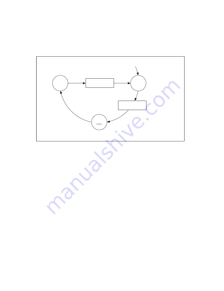
Figure 5-13 shows an output transfer in leading-edge mode. 

Figure 5-13.  Leading-Edge Mode Output

Leading-Edge Mode Timing Specifications

Figures 5-14 

and

5-15

 show the timing diagrams for leading-edge 

mode.

Wait

For

Data

Wait

For

REQ

Programmable

Delay

Programmable

Delay

Wait

For

REQ

When REQ

Asserted

When 6533 Device

Has Data to Output,

Output Data*

Clear

ACK

Pulse

When REQ
Unasserted

Initial State

ACK Cleared

Send

ACK

Pulse

* With REQ-edge latching enabled, the data written is

delayed until the next inactive-going REQ edge.

Summary of Contents for DIO 6533

Page 1: ...533 User Manual High Speed Digital I O Boards for PCI PXI CompactPCI AT EISA or PCMCIA Bus Systems July 1997 Edition Part Number 321464B 01 Copyright 1997 National Instruments Corporation All rights reserved ...

Page 2: ...5 76 26 00 Finland 09 725 725 11 France 01 48 14 24 24 Germany 089 741 31 30 Hong Kong 2645 3186 Israel 03 5734815 Italy 02 413091 Japan 03 5472 2970 Korea 02 596 7456 Mexico 5 520 2635 Netherlands 0348 433466 Norway 32 84 84 00 Singapore 2265886 Spain 91 640 0085 Sweden 08 730 49 70 Switzerland 056 200 51 51 Taiwan 02 377 1200 United Kingdom 01635 523545 National Instruments Corporate Headquarter...

Page 3: ... OF PRODUCTS OR INCIDENTAL OR CONSEQUENTIAL DAMAGES EVEN IF ADVISED OF THE POSSIBILITY THEREOF This limitation of the liability of National Instruments will apply regardless of the form of action whether in contract or tort including negligence Any action against National Instruments must be brought within one year after the cause of action accrues National Instruments shall not be liable for any ...

Page 4: ...s 1 1 Using PXI with CompactPCI 1 2 What You Need to Get Started 1 3 Software Programming Choices 1 4 National Instruments Application Software 1 4 NI DAQ Driver Software 1 5 Register Level Programming 1 6 Optional Equipment 1 7 Unpacking 1 8 Chapter 2 Installation and Configuration Software Installation 2 1 Hardware Installation 2 1 Installing the PCI DIO 32HS 2 1 Installing the PXI 6533 2 2 Inst...

Page 5: ...ction Triggers 3 6 Change Detection 3 7 Message Generation 3 8 Handshaking Protocols 3 8 8255 Emulation 3 9 Level ACK 3 9 Leading Edge Pulse 3 9 Long Pulse 3 9 Trailing Edge Pulse 3 9 Burst Mode 3 10 Comparing Protocols 3 10 Starting a Handshaking Transfer 3 12 Controlling the Startup Sequence 3 12 Controlling Line Polarities 3 13 Transfer Rates 3 13 Chapter 4 Signal Connections I O Connector 4 1 ...

Page 6: ...ng 5 3 Handshake Timing 5 4 8255 Emulation 5 4 Input 5 5 Output 5 6 8255 Emulation Mode Timing Specifications 5 8 Other Asynchronous Modes 5 9 Level ACK Mode 5 9 Input 5 9 Output 5 10 Level ACK Mode Timing Specifications 5 11 Leading Edge Mode 5 14 Input 5 14 Output 5 14 Leading Edge Mode Timing Specifications 5 16 Long Pulse Mode 5 19 Long Pulse Mode Timing Specifications 5 20 Trailing Edge Mode ...

Page 7: ...3 Block Diagram 3 4 Figure 3 4 Pattern Detection Example 3 7 Figure 4 1 6533 Device I O Connector Pin Assignments 4 2 Figure 4 2 RTSI Bus Signal Connection 4 9 Figure 4 3 Example of Data Signal Connections 4 11 Figure 4 4 Transmission Line Terminations 4 16 Figure 5 1 Pattern Generation Timing 5 1 Figure 5 2 Internal Request Timing 5 2 Figure 5 3 External Request Timing 5 3 Figure 5 4 Trigger Inpu...

Page 8: ...gure 5 22 Trailing Edge Mode Input Timing 5 26 Figure 5 23 Trailing Edge Mode Output Timing 5 27 Figure 5 24 Input Burst Mode Transfer Example 5 28 Figure 5 25 Output Burst Mode Transfer Example 5 29 Figure 5 26 Burst Mode Output Timing Default 5 30 Figure 5 27 Burst Mode Input Timing Default 5 31 Figure 5 28 Burst Mode Output Timing PCLK Reversed 5 32 Figure 5 29 Burst Mode Input Timing PCLK Reve...

Page 9: ...533 User Manual is organized as follows Chapter 1 Introduction describes the DIO 6533 DIO 32HS devices lists what you need to get started describes optional equipment and explains how to unpack your device Chapter 2 Installation and Configuration explains how to install and configure your DIO 6533 device Chapter 3 Hardware Overview provides an overview of the hardware functions of your DIO 6533 de...

Page 10: ... a bit or signal name for example DIOB 3 0 The symbol indicates that the text following it applies only to a specific DIO 6533 device bold italic Bold italic text denotes a note caution or warning 6533 device 6533 device refers to the PCI DIO 32HS PXI 6533 AT DIO 32HS and DAQCard 6533 devices unless otherwise noted italic Italic text denotes emphasis a cross reference or an introduction to a key c...

Page 11: ...lication software and NI DAQ software documentation National Instruments application software includes LabVIEW LabWindows CVI ComponentWorks and VirtualBench After you set up your hardware system use either your application software documentation or the NI DAQ documentation to help you write your application If you have a large complicated system it is worthwhile to look through the software docum...

Page 12: ...omments on our products and manuals We are interested in the applications you develop with our products and we want to help if you have problems with them To make it easy for you to contact us this manual contains comment and configuration forms for you to complete These forms are in Appendix C Customer Communication at the end of this manual ...

Page 13: ...nuous scatter gather DMA without requiring DMA resources from your computer See the Using PXI with CompactPCI section in this chapter for more information on your PXI 6533 device The AT DIO 32HS is a completely switchless jumperless DAQ device for AT 16 bit ISA buses The AT DIO 32HS implements the Plug and Play ISA Specification so that your operating system can configure all DMA channels interrup...

Page 14: ...industrial process monitoring and control For detailed 6533 device specifications see Appendix A Specifications Using PXI with CompactPCI Using PXI compatible products with standard CompactPCI products is an important feature provided by the PXI Specification rev 1 0 If you use a PXI compatible plug in device in a standard CompactPCI chassis you will be unable to use PXI specific functions but you...

Page 15: ...s still compatible as long as those pins on the sub bus are disabled by default and not ever enabled Damage may result if these lines are driven by the sub bus What You Need to Get Started To set up and use your DIO 6533 device you will need the following One of the following devices PCI DIO 32HS PXI 6533 AT DIO 32HS DAQCard 6533 DIO 6533 User Manual Table 1 1 Pins Used by the PXI 6533 Device PXI ...

Page 16: ...on VI Library a series of VIs for using LabVIEW with National Instruments DAQ hardware is included with LabVIEW The LabVIEW Data Acquisition VI Library is functionally equivalent to the NI DAQ software LabWindows CVI features interactive graphics and a state of the art user interface and uses the ANSI standard C programming language The LabWindows CVI Data Acquisition Library a series of functions...

Page 17: ... A D conversion buffered data acquisition high speed A D conversion analog output D A conversion waveform generation timed D A conversion digital I O counter timer operations SCXI RTSI calibration messaging and acquiring data to extended memory NI DAQ has both high level DAQ I O functions for maximum ease of use and low level DAQ I O functions for maximum flexibility and performance Examples for h...

Page 18: ...rogramming any National Instruments DAQ hardware is to write register level software Writing register level programming software can be very time consuming and inefficient and is not recommended for most users Even if you are an experienced register level programmer consider using NI DAQ or National Instruments application software to program your National Instruments DAQ hardware Using National I...

Page 19: ...w terminals Real Time System Integration RTSI bus cables SCXI modules and accessories for isolating digital signals controlling relays and creating isolated analog outputs Low channel count signal conditioning modules devices and accessories including relays and optical isolation Some cables and accessories require use of the 68 to 50 pin DIO 6533 device adaptor detailed in Appendix B Optional Ada...

Page 20: ...recautions Ground yourself via a grounding strap or by holding a grounded object Touch the antistatic package to a metal part of your computer chassis before removing the device from the package Remove the device from the package and inspect the device for loose components or any sign of damage Notify National Instruments if the device appears damaged in any way Do not install a damaged device int...

Page 21: ...struments application software packages refer to the appropriate release notes After you have installed your application software refer to your NI DAQ release notes and follow the instructions given there for your operating system and application software package Hardware Installation Following are general installation instructions for each device Consult your computer or chassis user manual or te...

Page 22: ...nnector lines for purposes other than PXI see Using PXI with CompactPCI in Chapter 1 Introduction of this manual 1 Turn off and unplug your PXI or CompactPCI chassis 2 Choose an unused PXI or CompactPCI 5 V peripheral slot For maximum performance install the PXI 6533 in a slot that supports bus arbitration or bus master cards The PXI 6533 contains onboard bus master DMA logic that can operate only...

Page 23: ...AT DIO 32HS to the back panel rail of the computer 7 Visually verify the installation 8 Replace the top cover of the computer 9 Plug in and turn on your computer Installing the DAQCard 6533 You can install your DAQCard 6533 in any available Type II PCMCIA slot in your computer See Figure 2 1 for the completed installation 1 Turn off your computer If your computer supports hot insertion you may ins...

Page 24: ...dy for software configuration PCI PXI and DAQCard Device Configuration The PCI DIO 32HS PXI 6533 and DAQCard 6533 are completely software configurable The system software automatically allocates all device resources including base memory address and interrupt level These devices do not require DMA controller resources from your computer PCMCIA Socket Portable Computer I O Cable CB 68 I O Signals ...

Page 25: ... and Play Configuration Manager The Configuration Manager receives all of the resource requests at startup compares the available resources to those requested and assigns the available resources as efficiently as possible to the Plug and Play devices Application software can query the Configuration Manager to determine the resources assigned to each device without your involvement The Plug and Pla...

Page 26: ...omputer and channels 0 1 2 3 5 6 and 7 in an EISA computer These selections are all software configured and do not require you to manually change any settings on the device Interrupt Channel Selection The AT DIO 32HS increases bus efficiency by using an interrupt channel for event notification The AT DIO 32HS can use interrupt channel 3 4 5 6 7 9 10 11 12 14 or 15 This selection is software config...

Page 27: ...3Com EtherLink default 310 to 31F 320 to 32F IBM PC XT Fixed Disk Controller 330 to 35F 360 to 363 PC Network low address 364 to 367 Reserved 368 to 36B PC Network high address 36C to 36F Reserved 370 to 366 PC AT Parallel Printer Port 1 LPT1 380 to 38C SDLC Communications 380 to 389 Bisynchronous BSC Communications alternate 390 to 393 Cluster Adapter 0 394 to 39F 3A0 to 3A9 BSC Communications pr...

Page 28: ... Plug and Play operation Table 2 2 PC AT Interrupt Assignment Map IRQ Device 15 Available 14 Fixed Disk Controller 13 Coprocessor 12 AT DIO 32F default 11 AT DIO 32F default 10 AT MIO 16 default 9 PC Network default PC Network Alternate default 8 Real Time Clock 7 Parallel Port 1 LPT1 6 Diskette Drive Controller Fixed Disk and Diskette Drive Controller 5 Parallel Port 2 LPT2 PC DIO 24 default Lab ...

Page 29: ...te Cluster primary PC Network PC Network Alternate WD EtherCard default 3Com EtherLink default 2 IRQ 8 15 Chain from interrupt controller 2 1 Keyboard Controller Output Buffer Full 0 Timer Channel 0 Output Table 2 3 PC AT 16 Bit DMA Channel Assignment Map Channel Device 7 AT MIO 16 Series default 6 AT MIO 16 Series default AT DIO 32F default 5 AT DIO 32F default 4 Cascade for DMA Controller 1 chan...

Page 30: ...e contains the National Instruments DAQ DIO chip a 32 bit general purpose digital I O interface The DAQ DIO chip enables the 6533 device to perform single line and single point input and output digital data acquisition digital waveform generation and high speed data transfer using a wide range of handshaking protocols Figures 3 1 3 2 and 3 3 show the block diagrams for the 6533 devices ...

Page 31: ... Diagram DAQ DIO Counters and Timers DMA Interrupt Requests Handshaking and Control Data Latches and Drivers Data Lines Data Lines 32 32 MITE PCI Interface PCI I O Channel EEPROM 20 MHz RTSI RTSI PXI Trigger Bus Oscillator Interface Control Lines 8 I O Connector Clock Selection Internal FIFOs Bus Interface Request Processing ...

Page 32: ...agram DAQ DIO Counters and Timers DMA Interrupt Requests Handshaking and Control Data Latches and Drivers Data Lines Data Lines 32 16 AT Plug and Play Interface AT I O Channel EEPROM 20 MHz RTSI RTSI Bus Oscillator Interface Control Lines 8 I O Connector Clock Selection Internal FIFOs Bus Interface Request Processing ...

Page 33: ... A B C and D You can configure each line individually for either input or output When you perform only unstrobed I O the 6533 device does not require its handshaking control and status signals to carry timing information Therefore you can use the REQ and STOPTRIG lines as extra data inputs and the ACK and PCLK lines as extra data outputs DAQ DIO Counters and Timers DMA Interrupt Requests Handshaki...

Page 34: ...group has its own independent set of timing control lines ACK STARTTRIG REQ PCLK and STOPTRIG to carry control status clocking and trigger information Any external device that the 6533 devices control monitor test or communicate with is referred to as a peripheral device Strobed operations fall into two categories pattern generation and full or two way handshaking transfer In pattern generation da...

Page 35: ...se fixed rates are not critical you can run full handshaking operations at the highest possible speeds Pattern and Change Detection You can configure the 6533 device to do several types of pattern and change detection These modes add additional monitoring capabilities to strobed input operation Pattern Detection Triggers You can configure the 6533 device to search for a particular pattern in the i...

Page 36: ...ccurs during line switching does not falsely cause a match A glitch must be present for no more than 20 ns to guarantee rejection A valid pattern must be present for at least 60 ns to guarantee detection In strobed request based pattern detection data is checked as it is strobed in by request pulses Strobed pattern detection is typically used to generate triggers You can use strobed pattern detect...

Page 37: ...change and pattern detection masks are the same input lines that are significant for pattern detection are also significant for change detection Message Generation Some software environments such as LabVIEW and LabWindows CVI support message generation Messages allow you to run a user specified routine when a particular data acquisition event occurs For example Generate a message upon acquisition ...

Page 38: ...k transfer rate of any protocol except burst mode Level ACK After each transfer the 6533 device asserts the ACK signal to the peripheral device Holding the ACK line at the asserted level the 6533 device does not begin a new transfer until a false to true transition on the REQ line from the peripheral device occurs Leading Edge Pulse After each transfer the 6533 device sends a pulse on the ACK line...

Page 39: ...e shares a clock signal between the 6533 device and the peripheral device Table 3 1 shows peak handshaking rates for typical cable lengths The peak rates give an upper limit deriving from the pulse widths and other timing specifications of the handshaking protocol Your actual maximum rate depends on many factors see the Transfer Rates section in this chapter Table 3 1 also shows whether the ACK an...

Page 40: ...Leading Before ACK and between transfers Leading Edge Pulse Long Pulse 3 33 2 5 Programmable Leading For pulse width and between transfers Long Pulse 8255 Emula tion PC DIO 24 PC DIO 96 PnP 8255 82C55 Trailing EdgePulse 1 8 1 5 Programmable Trailing For pulse width and between transfers Trailing Edge Pulse Synchronous Protocol Burst 20 10 Programmable Neither level REQ For clock speed Burst Althou...

Page 41: ...figured and is driving a valid REQ value before you enable the transfer on the 6533 device To use a prescribed initialization order perform the following steps 1 Configure the 6533 device for a protocol compatible with your peripheral device 2 Configure and reset the peripheral device if appropriate 3 Enable the input device 6533 device or peripheral device and begin a transfer 4 Enable the output...

Page 42: ...e 6533 device can achieve for two way handshaking applications is the lower of the following two rates The peak handshaking rate from Table 3 1 which can be lowered by the handshaking speed of your peripheral device The average available bus bandwidth based on your computer system the number of other devices generating bus cycles and your application software The maximum sustainable transfer rate ...

Page 43: ...tration use software to select interrupt driven transfers The AT DIO 32HS supports DMA if system DMA resources are available If a second DMA channel is available you can minimize channel reprogramming time by allocating two DMA channels to a single transfer By allocating two channels you allow the AT DIO 32HS software to reprogram one channel while continuing transfers on the other channel This is...

Page 44: ...e adapter you can also connect your 6533 device to 50 pin accessories through an NB1 ribbon cable I O Connector Figure 4 1 shows the pin assignments for the 68 pin 6533 device I O connector Refer to Appendix B Optional Adapter Description for the pin assignments for the 68 to 50 pin adapter Caution Connections that exceed any of the maximum input or output ratings on the 6533 may damage your devic...

Page 45: ...it allows you to connect one device s ACK pin to the 5 V REQ1 ACK1 STARTTRIG1 STOPTRIG1 PCLK1 PCLK2 STOPTRIG2 ACK2 STARTTRIG2 REQ2 DIOA0 GND DIOA3 DIOA4 GND DIOA7 DIOB0 DIOB1 GND RGND GND DIOB6 DIOB7 DIOC0 GND DIOC3 DIOC4 GND DIOC7 DIOD0 GND DIOD3 DIOD4 GND DIOD7 RGND GND DPULL CPULL GND GND RGND GND GND DIOA1 DIOA2 GND DIOA5 DIOA6 GND GND DIOB2 DIOB3 DIOB4 DIOB5 GND RGND DIOC1 DIOC2 GND DIOC5 DIO...

Page 46: ...arries timing pulses either to or from the peripheral to strobe data into or out of the 6533 device These strobe signals are comparable to the CONVERT or UPDATE signals of an analog DAQ device When not configuring the 6533 device for group operations you can use the REQ 1 2 lines as extra general purpose input lines IN 3 4 3 8 ACK 1 2 Control Group 1 and group 2 acknowledge lines In handshaking mo...

Page 47: ...device for group operations you can use the PCLK 1 2 lines as extra general purpose output lines OUT 1 2 10 12 13 15 44 45 47 48 DIOA 0 7 Data Port A bidirectional data lines Port A is port number 0 DIOA7 is the MSB DIOA0 is the LSB When combined in a group with other ports port A is the least significant port 16 17 21 22 51 54 DIOB 0 7 Data Port B bidirectional data lines Port B is port number 1 ...

Page 48: ...when undriven If you connect DPULL to 5 V the 6533 device pulls the data lines up If you connect DPULL to GND or leave DPULL unconnected the 6533 device pulls the data lines down 1 5 V Power 5 Volts output This line provides a maximum of 1 A of power regulated by an onboard fuse that can automatically reset itself after current returns to normal 11 14 18 20 24 27 30 33 36 37 41 42 46 49 50 55 59 6...

Page 49: ...rol and data lines begin at high impedance With no load attached the voltage levels of the lines are controlled by the pull up or pull down resistors Pull up pull down Control lines All timing control lines have 2 2 kΩ pull up or pull down resistors controlled by the CPULL line Data lines All timing data lines have 100 kΩ pull up or pull down resistors controlled by the DPULL line Bias selection l...

Page 50: ...cabled together inside a computer to share these signals The PXI 6533 uses pins on the PXI J2 connector to connect the RTSI bus to the PXI trigger bus as defined in the PXI Specification rev 1 0 All National Instruments PXI boards that provide a connection to these pins can be connected together by software This feature is available only when the PXI 6533 is used in a PXI compatible chassis It is ...

Page 51: ...er device that uses a 20 MHz clock The 20 MHz timebase whether local or imported from the RTSI bus serves as the primary frequency source for the 6533 device You can select a clocking configuration through software By default the 6533 device uses its own internal timebase without driving the RTSI bus clock line PXI 6533 The PXI 6533 uses PXI trigger line 7 as its RTSI clock line RTSI Triggers The ...

Page 52: ...rigger bus lines 0 through 6 Data Signal Connections The digital data signals are DIOA 0 7 DIOB 0 7 DIOC 0 7 and DIOD 0 7 These data signals are referenced to the GND pins Ports DIOA DIOB DIOC and DIOD are port numbers 0 1 2 and 3 respectively RTSI Bus or PXI Connector Crossbar Switch Trigger 20 MHz Timebase REQ 1 2 ACK 1 2 STARTTRIG 1 2 PCLK 1 2 DAQ DIO STOPTRIG 1 2 Switch 7 2 2 2 2 ...

Page 53: ...4 3 shows DIOA 0 3 configured for input DIOA 4 7 configured for standard output and DIOB 0 3 configured for wired OR output Unstrobed input applications include sensing external device states such as the state of the switch shown in the figure and receiving low speed TTL signals Unstrobed output applications include driving external controls and indicators such as the LED shown in Figure 4 3 and s...

Page 54: ...tional Instruments Corporation 4 11 DIO 6533 User Manual Figure 4 3 Example of Data Signal Connections LED 5 V TTL Signal 5 V DIOA 4 7 DIOB 0 3 DIOA 0 3 GND Switch I O Connector GND 5 V Switch DPULL 5 V Open Collector TTL 6533 Device ...

Page 55: ...he 5 V pin making the 6533 device 100 kΩ pull down resistors into 100 kΩ pull up resistors A wired OR driver has the following advantages over a standard driver You can connect two or more wired OR outputs together without damaging the drivers You can connect wired OR outputs to open collector drivers to GND signals or to switches connecting to GND signals without damaging the drivers You can use ...

Page 56: ... control and data signals If you drive the CPULL pin low connect the CPULL pin to a GND pin or leave the CPULL line disconnected the 6533 device pulls all its control lines down to 0 V with 2 2 kΩ resistors If you drive the CPULL pin high or connect the CPULL pin to the 5 V pin the 6533 device pulls all its control lines to 5 V with the same 2 2 kΩ resistors Similarly if you drive the DPULL pin lo...

Page 57: ...32HS Power rating 4 65 to 5 25 VDC at 1 A DAQCard 6533 Power rating 4 65 to 5 25 VDC at 250 mA You can connect the 5 V pin to the CPULL and DPULL pins to control the bias of the 6533 device control and data pins as described in the Pull Up and Pull Down Connections section in this chapter Caution Do not connect the 5 V power pin directly to the GND RGND or any output pin of the 6533 device or any ...

Page 58: ...ion lines A good method for the 6533 device is to connect one fast Schottky diode from 5 V to each signal line and another from the signal line to ground The 5 V and ground connections should be low impedance connections For example if you make your 5 V connection through a long wire back to the 5 V pin of the 6533 device add a capacitor to your termination circuit to stabilize the 5 V connection ...

Page 59: ...g currents in or voltages on the 6533 device signal lines if they run in parallel paths at a close distance To reduce the magnetic coupling between lines separate them by a reasonable distance if they run in parallel or run the lines at right angles to each other Do not run signal lines through conduits that also contain power lines Protect signal lines from magnetic fields caused by electric moto...

Page 60: ... into or out of the 6533 device You can use up to two additional timing signals if you select triggered pattern generation a start trigger and a stop trigger A start trigger if used begins the pattern generation operation A stop trigger ends the operation However you can specify a number of data points to transfer after the stop trigger You can substitute a digital pattern for either the start or ...

Page 61: ...W you specify an overall period and the software selects the interval and timebase Figure 5 2 Internal Request Timing External Requests Figure 5 3 shows external request timing The request signal must pulse low and return high The request pulse low and high durations must be at least 20 ns each The minimum period is 50 ns Parameter Description tc Cycle time tlw Width of low pulse tp Propagation ti...

Page 62: ...ze of your buffer The start trigger is a second trigger that begins a pattern generation operation If you do not enable a start trigger the operation starts immediately when you issue a software command to perform a transfer Triggers are available for both waveform generation output mode and data acquisition input mode Acquiring data that occurs before or after a trigger is known as pretrigger or ...

Page 63: ...Overview for more information about pattern detection Handshake Timing This section describes the 6533 device two way handshaking modes and the timing specifications of each mode In handshaking the ACK signal always conveys information about when the 6533 device is ready for a transfer The REQ signal conveys information about when the peripheral device is ready for a transfer Note Depending on the...

Page 64: ...k transfers much faster than a true 8255 based device If your peripheral device requires more time between transfers you can configure the 6533 device to add a data settling delay between transfers You can use a 6533 device in emulation mode with 8 16 or 32 bit data paths Input Note 6533 device terminology differs from 8255 terminology In input mode the 6533 device REQ line carries the 8255 STB in...

Page 65: ...erward the 6533 device reasserts the ACK signal low when ready for another input Figure 5 5 shows an input transfer in 8255 emulation mode Figure 5 5 8255 Emulation Mode Input Output Note 6533 device terminology differs from 8255 terminology In output mode the 6533 device REQ line carries the 8255 ACK input signal and the 6533 device ACK line carries the 8255 OBF output signal Both lines are activ...

Page 66: ...dge causes the ACK signal to return to the inactive state and the rising REQ signal edge enables a new transfer to occur Therefore the peripheral device should wait until it has received data before raising the REQ signal The peripheral device can also wait for the ACK signal to deassert before raising the REQ signal Figure 5 6 shows an output transfer in 8255 emulation mode Figure 5 6 8255 Emulat...

Page 67: ...s tr r REQ low duration 75 trr REQ high duration 75 ta r ACK falling edge to REQ rising edge 0 tdir Input data valid to REQ rising edge 0 trdi REQ rising edge to input data invalid 10 Output Parameters taa ACK high duration 100 tr a REQ falling edge to ACK rising edge 150 tdoa Output data valid to ACK falling edge 25 trdo REQ rising edge to output data invalid 100 All timing values are in nanoseco...

Page 68: ...uest edge latching With request edge latching enabled in input mode the 6533 device latches data in from the I O connector on the REQ edge before reading the data In output mode after writing the data the 6533 device latches data out of the I O connector on the REQ edge Which edge of REQ is used rising or falling depends on the handshaking mode and the REQ polarity Level ACK Mode In level ACK mode...

Page 69: ...e to deassert the ACK signal and request additional data To slow down the handshake you can specify a data settling delay to occur before the ACK signal This delay increases the setup time from valid output data to the ACK signal Figure 5 8 shows an input transfer in level ACK mode Figure 5 8 Level ACK Mode Input Wait For Space Wait For REQ Programmable Delay Programmable Delay Wait For REQ When R...

Page 70: ...ng Specifications Figures 5 10 and 5 11 show the timing diagrams for level ACK mode Wait For Data Wait For REQ Programmable Delay Programmable Delay Wait For REQ When REQ Asserted Clear ACK When 6533 Device Has Data to Output Output Data When REQ Unasserted Initial State ACK Cleared Send ACK With REQ edge latching enabled the data written is delayed until the next inactive going REQ edge ...

Page 71: ...ta setup to REQ active with REQ edge latching 0 trdi Input data hold from REQ active with REQ edge latching 10 tdir 2 Input data setup to REQ with REQ edge latching disabled 0 tadi Input data hold from ACK with REQ edge latching disabled 0 Output Parameters taa ACK pulse width 225 tra REQ to ACK inactive 100 200 All timing values are in nanoseconds REQ ACK Input Data REQ edge latching Input Data R...

Page 72: ...0 Output Parameters taa ACK pulse width 225 tra REQ to ACK inactive 100 200 tr do REQ inactive to new output data with REQ edge latching 0 50 trdo REQ to new output data with REQ edge latching disabled 0 tdoa Output data valid to ACK with REQ edge latching disabled 251 1 tdoa min 25 programmable delay All timing values are in nanoseconds REQ ACK Output Data REQ edge latching Output Data REQ edge l...

Page 73: ... the REQ signal The 6533 device sends another ACK pulse when ready for another input To slow down the handshake you can specify a data settling delay to occur before the ACK signal Output In output mode the 6533 device sends an ACK pulse after driving output data to indicate new valid output data The ACK pulse width is fixed assuming the peripheral device has deasserted the REQ signal Otherwise th...

Page 74: ... Figure 5 12 Leading Edge Mode Input Wait For Space Wait For REQ Programmable Delay Programmable Delay Wait For REQ When REQ Asserted When 6533 Device Has Space For Data Input Data Clear ACK Pulse When REQ Unasserted Initial State ACK Cleared Send ACK Pulse With REQ edge latching enabled the data read is from the last active going REQ edge ...

Page 75: ... Specifications Figures 5 14 and 5 15 show the timing diagrams for leading edge mode Wait For Data Wait For REQ Programmable Delay Programmable Delay Wait For REQ When REQ Asserted When 6533 Device Has Data to Output Output Data Clear ACK Pulse When REQ Unasserted Initial State ACK Cleared Send ACK Pulse With REQ edge latching enabled the data written is delayed until the next inactive going REQ e...

Page 76: ... setup to REQ active with REQ edge latching 0 trdi Input data hold from REQ active with REQ edge latching 10 tdir 2 Input data setup to REQ with REQ edge latching disabled 0 tadi Input data hold from ACK with REQ edge latching disabled 0 Output Parameters taa ACK pulse width 125 tr a REQ inactive to ACK inactive 150 All timing values are in nanoseconds REQ ACK Input Data REQ edge latching disabled...

Page 77: ...Output Parameters taa ACK pulse width 125 tr a REQ inactive to ACK inactive 150 tr do REQ inactive to new output data with REQ edge latching 0 50 trdo REQ to new output data with REQ edge latching disabled 0 tdoa Output data valid to ACK with REQ edge latching disabled 251 1 tdoa min 25 programmable delay All timing values are in nanoseconds REQ ACK Output Data REQ edge latching Output Data REQ ed...

Page 78: ...de if you set the ACK and REQ signals to active low If you want to use long pulse mode to handshake with an actual 8255 or 82C55 PPI make sure you select an adequate minimum pulse width for your 8255 or 82C55 A data settling delay of 500 ns is sufficient for any current 8255 or 82C55 PPI Figures 5 16 and 5 17 show long pulse mode input and output diagrams respectively Figure 5 16 Long Pulse Mode I...

Page 79: ...nd 5 19 show the timing diagrams for long pulse mode Wait For Data Wait For REQ Programmable Delay Programmable Delay Wait For REQ When REQ Asserted When 6533 Device Has Data to Output Output Data Clear ACK Pulse When REQ Unasserted Initial State ACK Cleared Send ACK Pulse With REQ edge latching enabled the data written is delayed until the next inactive going REQ edge ...

Page 80: ...ve with REQ edge latching 0 trdi Input data hold from REQ active with REQ edge latching 10 tdir 2 Input data setup to REQ with REQ edge latching disabled 0 tadi Input data hold from ACK with REQ edge latching disabled 0 Output Parameters taa ACK pulse width 1251 tr a REQ inactive to ACK inactive 150 1 taa min 125 programmable delay All timing values are in nanoseconds REQ ACK Input Data REQ edge l...

Page 81: ...ar ACK to next REQ 0 Output Parameters taa ACK pulse width 1251 tr do REQ inactive to new output data with REQ edge latching 0 50 trdo REQ to new output data with REQ edge latching disabled 0 tdoa Output data valid to ACK with REQ edge latching disabled 25 1 taa min 125 programmable delay All timing values are in nanoseconds REQ ACK Output Data REQ edge latching Output Data REQ edge latching disab...

Page 82: ...EQ signal The 6533 device sends another ACK pulse when ready for another input To slow down the handshake you can specify a data settling delay to increase the ACK pulse width Output In output mode the 6533 device sends an ACK pulse of programmable width after driving output data to indicate new valid output data The peripheral device can latch the data on the falling or rising edge of the ACK sig...

Page 83: ... mode Figure 5 20 Trailing Edge Mode Input Wait For Space Wait For REQ Programmable Delay Programmable Delay Wait For REQ When REQ Unasserted When 6533 Device Has Space For Data Input Data Clear ACK When REQ Asserted Send ACK Initial State ACK Cleared With REQ edge latching enabled the data read is from the last inactive going REQ edge ...

Page 84: ...Timing Specifications Figures 5 22 and 5 23 show the timing diagrams for trailing edge mode Wait For Data Wait For REQ Programmable Delay Programmable Delay Wait For REQ When REQ Unasserted When 6533 Device Has Data to Output Output Data Clear ACK When REQ Asserted Initial State ACK Cleared Send ACK With REQ edge latching enabled the data written is delayed until the next inactive going REQ edge ...

Page 85: ... di Input data hold from REQ inactive with REQ edge latching 10 tdir Input data setup to REQ with REQ edge latching disabled 0 tadi Input data hold from ACK with REQ edge latching disabled 0 Output Parameters taa ACK pulse width 2251 2752 ta r ACK inactive to next REQ inactive 0 1 taa min 225 programmable delay All timing values are in nanoseconds 2 taa max 275 programmable delay REQ ACK Input Dat...

Page 86: ... peripheral device can insert wait states into the protocol by Parameter Description Minimum Maximum Input Parameters trr REQ pulse width 75 tr r REQ inactive duration 75 ta r ACK inactive to next REQ inactive 0 Output Parameters taa ACK pulse width 2251 2752 tr do 1 REQ inactive to new output data with REQ edge latching 0 50 tr do 2 REQ inactive to new output data with REQ edge latching disabled ...

Page 87: ...rection is the opposite of the data direction any delay associated with the cable between the 6533 device and the peripheral device increases the data hold time available although decreasing the data setup time If necessary for long cables you can compensate for the decrease in data setup time by slowing down the PCLK clock Burst Mode Timing Specifications Figure 5 24 shows a burst mode transfer d...

Page 88: ...Chapter 5 Signal Timing National Instruments Corporation 5 29 DIO 6533 User Manual Figure 5 25 Output Burst Mode Transfer Example PCLK ACK REQ Data Out D1 D2 D3 D4 D5 ...

Page 89: ...K high pulse duration 20 tpl PCLK low pulse duration 20 trs Setup time from REQ valid to PCLK falling edge 1 trh Hold time from PCLK to REQ invalid 0 Output Parameters tpa PCLK to ACK valid 22 tah Hold time from PCLK to ACK invalid 3 tpdo PCLK to output data valid 28 tdoh Hold time from PCLK to output data invalid 5 All timing values are in nanoseconds PCLK ACK Data Out REQ trs tpa tpdo tpw tpl tp...

Page 90: ...ime from input data valid to PCLK 4 tdih Hold time from PCLK to input data invalid 6 Output Parameters tpc PCLK cycle time 50 7001 tpw PCLK high pulse duration tpc 2 5 tpc 2 5 tpa PCLK to ACK valid 18 tah Hold time from PCLK to ACK invalid 3 1 tpc programmable delay from 100 to 700 ns or 50 ns if programmable delay is 0 Timebase stability for the onboard 20 MHz clock source is 50 ppm All timing va...

Page 91: ...utput Parameters tpc PCLK cycle time 50 7001 tpw PCLK high pulse duration tpc 2 5 tpc 2 5 tpa PCLK to ACK valid 18 tah Hold time from PCLK to ACK invalid 3 tpdo PCLK to output data valid 28 tdoh Hold time from PCLK to output data invalid 4 1tpc programmable delay from 100 to 700 ns or 50 ns if programmable delay is 0 Timebase stability for the board 20 MHz clock source is 50 ppm All timing values ...

Page 92: ...put Parameters tpc PCLK cycle time 50 tpw PCLK high pulse duration 20 tpl PCLK low pulse duration 20 trs Setup time from REQ valid to PCLK falling edge 1 trh Hold time from PCLK to REQ invalid 0 Output Parameters tpa PCLK to ACK valid 22 tah Hold time from PCLK to ACK invalid 3 All timing values are in nanoseconds PCLK ACK Data In REQ tdis tdih trs tpa tpw tpl tpc trh tah ...

Page 93: ...hese specifications are typical at 25 C unless otherwise noted PCI DIO 32HS PXI 6533 AT DIO 32HS and DAQCard 6533 Devices Digital I O Number of channels 32 input output 4 dedicated output and control 4 dedicated input and status Compatibility TTL CMOS standard or wired OR1 Hysteresis 500 mV 1 As of NI DAQ 5 1 LabVIEW does not support wired OR outputs ...

Page 94: ...r data lines Vin 0 4 V DPULL high DPULL low 70 µA 10 µA Input high current for data lines Vin 2 4 V DPULL high DPULL low 10 µA 40 µA Input low current for control lines Vin 0 4 V CPULL high CPULL low 2 5 mA 200 µA Input high current for control lines Vin 2 4 V CPULL high CPULL low 200 µA 1 4 mA Input low current for CPULL DPULL Vin 0 4 V 4 µA Input high current for CPULL DPULL Vin 2 4 V 140 µA ...

Page 95: ... stated pulled up or down selectable Data transfers Programmed I O DMA Strobed I O Pattern Generation Direction Input or output Modes Internally or externally timed Output low voltage IOL 24 mA 0 4 V Output high voltage IOH 24 mA 2 4 V When configured as standard outputs Drivers configured as wired OR outputs are tri stated when logically high Level Min Max ...

Page 96: ...S Rates in MS s MB s on Sample Systems 32 bit input 2 8 11 2 4 16 4 16 16 bit input 4 8 5 10 6 67 13 33 8 bit input 6 67 6 67 10 10 10 10 32 bit output 1 4 2 8 3 33 13 33 16 bit output 1 2 2 5 5 3 33 6 67 8 bit output 2 2 5 5 6 67 6 67 PXI 6533 Rates in MS s MB s on Sample Systems 32 bit input 4 16 16 bit input 5 10 8 bit input 6 67 6 67 32 bit output 2 22 8 88 16 bit output 2 5 5 8 bit output 5 5...

Page 97: ...S Natoma rates were measured on a 180 MHz Pentium Pro system with the Natoma 440FX chip set The PXI 6533 rates were measured using a 133MHz Pentium CompactPCI controller with the Triton I chip set The AT DIO 32HS rates were measured using the dual DMA transfer method on a 100 MHz Pentium computer with the Triton I 430FX chip set The DAQCard 6533 Triton I rates were measured using a 75 MHz Pentium ...

Page 98: ...l performing continuous waveform generation using 100 000 point or larger buffers with no other DAQ operations in progress The PCI DIO 32HS PXI 6533 and AT DIO 32HS handshaking rates are DMA based and do not necessarily increase as the speed of the computer increases The PCI DIO 32HS and AT DIO 32HS rates shown were measured on a sample 100 MHz Intel Pentium based computer with an Intel 430FX Trit...

Page 99: ...hange detection resolution 150 ns Triggers Start and Stop Triggers Compatibility TTL CMOS Trigger types Rising or falling edge or digital pattern Pulse width for edge triggers min 10 ns Pattern triggers detection capabilities Detect pattern match or mismatch on user selected bits RTSI Triggers PCI PXI AT Trigger lines 7 75 MHz Pentium 133 MHz Pentium 266 MHz Pentium II Rates in KB s kS s on Sample...

Page 100: ...l DMA DAQCard 6533 type PCMCIA slave Power Requirement 5 VDC 5 with light output load 500 mA Power available at I O connector PCI DIO 32HS PXI 6533 and AT DIO 32HS 4 65 to 5 25 VDC at 1 A DAQCard 6533 4 65 to 5 25 VDC at 250 mA Physical Dimensions not including connectors 17 5 by 10 7 cm 6 9 by 4 2 in I O connector PCI DIO 32HS PXI 6533 and AT DIO 32HS 68 pin male SCSI II type DAQCard 6533 68 pin ...

Page 101: ...s 3 per Section 4 5 5 4 1 Half sine shock pulse 11 ms duration 30 g peak 30 shocks per face Operational random vibration 5 to 500 Hz 0 31 grms 3 axes Nonoperational random vibration 5 to 500 Hz 2 5 grms 3 axes Note Random vibration profiles were developed in accordance with MIL T 28800E and MIL STD 810E Method 514 Test levels exceed those recommended in MIL STD 810E for Category 1 Basic Transporta...

Page 102: ...equire an AT DIO 32F pinout The adapter connects directly to a PCI DIO 32HS PXI 6533 or AT DIO 32HS device Using a PSHR68 68M shielded cable you can also connect the adapter to a DAQCard 6533 device The female side of the adapter connects directly to the PCI DIO 32HS PXI 6533 or AT DIO 32HS device or to the PSHR68 68M cable The male side of the adapter provides the pin assignments shown in Figure ...

Page 103: ... REQ1 PCLK1 OUT1 STOPTRIG1 IN1 ACK1 GND GND GND GND GND DIOC6 DIOC2 DIOC3 DIOC5 DIOD2 DIOD6 DIOD3 DIOD1 DIOB1 DIOB6 DIOB2 DIOA3 DIOA2 DIOA6 GND DIOB3 DIOA5 GND GND GND GND REQ2 PCLK2 OUT2 STOPTRIG2 IN2 ACK2 DIOC4 DIOC0 DIOC1 DIOC7 DIOD5 DIOD7 DIOD0 DIOD4 49 50 47 48 45 46 43 44 41 42 39 40 37 38 35 36 33 34 31 32 29 30 27 28 25 26 23 24 21 22 19 20 17 18 15 16 13 14 11 12 9 10 7 8 5 6 3 4 1 2 ...

Page 104: ...ms does not answer your questions we offer fax and telephone support through our technical support centers which are staffed by applications engineers Electronic Services National Instruments has BBS and FTP sites dedicated for 24 hour support with a collection of files and documents to answer most common customer questions From these sites you can also download the latest instrument drivers updat...

Page 105: ...ed your software to obtain support Telephone Fax Australia 03 9879 5166 03 9879 6277 Austria 0662 45 79 90 0 0662 45 79 90 19 Belgium 02 757 00 20 02 757 03 11 Canada Ontario 905 785 0085 905 785 0086 Canada Quebec 514 694 8521 514 694 4399 Denmark 45 76 26 00 45 76 26 02 Finland 09 725 725 11 09 725 725 55 France 01 48 14 24 24 01 48 14 24 14 Germany 089 741 31 30 089 714 60 35 Hong Kong 2645 318...

Page 106: ...________________________________________________ _______________________________________________________________________________ National Instruments hardware product model __________ Revision ______________________ Configuration ___________________________________________________________________ National Instruments software product ____________________________Version ____________ Configuration _...

Page 107: ..._______________________________________________ Base I O address of other boards _____________________________________________________ DMA channels of other boards ______________________________________________________ Interrupt level of other boards _______________________________________________________ Other Products Computer make and model ______________________________________________________...

Page 108: ...________________________________________________ _______________________________________________________________________________ _______________________________________________________________________________ _______________________________________________________________________________ _______________________________________________________________________________ _______________________________...

Page 109: ...ents Corporation G 1 DIO 6533 User Manual Glossary Symbols degree negative of or minus Ω ohm per percent plus or minus positive of or plus Prefix Meaning Value m milli 10 3 µ micro 10 6 n nano 10 9 k kilo 103 M mega 106 ...

Page 110: ... binary number Also used to denote the amount of memory required to store one byte of data base address a memory address that serves as the starting address for programmable registers All other addresses are located by adding to the base address bus the group of conductors that interconnect individual circuitry in a computer Typically a bus is the expansion vehicle to which I O or other devices ar...

Page 111: ...r and possibly generating control signals with D A and or DIO boards in the same computer DC direct current device a plug in data acquisition board card or pad that can contain multiple channels and conversion devices Plug in boards PCMCIA cards and devices such as the DAQPad 1200 which connects to your computer parallel port are all examples of DAQ devices SCXI modules are distinct from devices w...

Page 112: ...ustry standard architecture event the condition or state of an analog or digital signal external trigger a voltage pulse from an external source that triggers an event such as A D conversion F FIFO first in first out memory buffer the first data stored is the first data sent to the acceptor FIFOs are often used on DAQ devices to temporarily store incoming or outgoing data until that data can be re...

Page 113: ...cal components of a computer system such as the circuit boards plug in boards chassis enclosures peripherals cables and so on hardware triggering a form of triggering where you set the start time of an acquisition and gather data at a known position in time relative to a trigger signal hex hexadecimal Hz hertz the number of scans read or updates written per second I IBM International Business Mach...

Page 114: ...t high IOL current output low IRQ interrupt request signal ISA industry standard architecture K kbytes s a unit for data transfer that means 1 000 or 103 bytes s kS 1 000 samples Kword 1 024 words of memory L LabVIEW laboratory virtual instrument engineering workbench latched digital I O See strobed digital I O LED light emitting diode LSB least significant bit M m meters max maximum MB megabytes ...

Page 115: ...I O O operating system base level software that controls a computer runs programs interacts with users and communicates with installed hardware or peripheral devices optical isolation the technique of using an optoelectric transmitter and receiver to transfer data without electrical continuity to eliminate high potential differences and transients P pattern generation a type of strobed digital I O...

Page 116: ... a communications connection on a computer or a remote controller 2 a digital port consisting of four or eight lines of digital input and or output posttrigger acquisition the technique used on a DAQ board to acquire a programmed number of samples after trigger conditions are met PPI programmable peripheral interface ppm parts per million pretrigger acquisition the technique used on a DAQ board to...

Page 117: ...al input or output in which hardware uses timing signals to regulate the rate of input or output Types of strobed digital I O include handshaking and pattern generation switchless device devices that do not require dip switches or jumpers to configure resources on the devices also called Plug and Play devices synchronous hardware a property of an event that is synchronized to a reference clock T t...

Page 118: ...s in an update is equal to the number of channels in the output group For example one pulse from the update clock produces one update which sends one new sample to every analog output channel in the group V V volts Vcc the voltage of the power supply from the computer approximately 5 V VDC volts direct current VIH volts input high VIL volts input low Vin volts in VOH volts output high VOL volts ou...

Page 119: ...Also called an open collector or open drain driver word the standard number of bits that a processor or memory manipulates at one time Microprocessors typically use 8 16 or 32 bit words working voltage the highest voltage that should be applied to a product in normal use normally well under the breakdown voltage for safety margin ...

Page 120: ...n 2 5 to 2 9 base I O address selection 2 6 DMA channel selection 2 6 interrupt channel selection 2 6 to 2 9 Plug and Play mode 2 5 switchless data acquisition 2 5 AT DIO 32HS block diagram 3 3 installation 2 3 overview 1 1 B base I O address selection 2 6 bulletin board support C 1 burst mode 5 27 to 5 33 purpose and use 3 10 5 27 to 5 28 timing specifications 5 28 to 5 33 input mode transfer exa...

Page 121: ...ter level programming 1 6 unpacking 1 8 using PXI with CompactPCI 1 2 to 1 3 DIOA 0 7 signal description table 4 4 unstrobed I O 4 10 to 4 11 DIOB 0 7 signal description table 4 4 unstrobed I O 4 10 to 4 11 DIOC 0 7 signal table 4 4 DIOD 0 7 signal table 4 4 DMA channel selection PC AT 16 bit DMA channel assignment map table 2 9 software configured 2 6 documentation conventions used in manual xii ...

Page 122: ...ng protocols 3 10 to 3 11 definition 3 5 handshaking protocols 3 8 to 3 10 pattern and change detection 3 6 to 3 8 starting handshaking transfer 3 12 to 3 13 transfer rates 3 13 to 3 14 achieving highest possible rates 3 13 to 3 14 maximum 3 13 I I O connector 4 1 to 4 9 control signal summary 4 7 exceeding maximum ratings note 4 1 pin assignments table 4 2 RTSI bus interface 4 7 to 4 9 signal cha...

Page 123: ...ern generation timing 5 1 to 5 4 example figure 5 1 overview 5 1 request timing 5 2 to 5 3 external requests 5 2 to 5 3 internal requests 5 2 trigger timing 5 3 to 5 4 PC AT devices See AT device configuration PCI DIO 32HS block diagram 3 2 configuration 2 4 installation 2 1 to 2 2 overview 1 1 PCLK 1 2 signal control signal summary table 4 7 description table 4 4 peripheral device 3 5 physical sp...

Page 124: ...level ACK mode 5 9 to 5 14 long pulse mode 5 19 to 5 22 trailing edge mode 5 23 to 5 27 pattern generation timing 5 1 to 5 4 example figure 5 1 overview 5 1 request timing 5 2 to 5 3 trigger timing 5 3 to 5 4 software installation 2 1 software programming choices 1 4 to 1 6 National Instruments application software 1 4 to 1 5 NI DAQ driver software 1 5 to 1 6 register level programming 1 6 specifi...

Page 125: ...nd fax support C 2 termination and field wiring 4 14 to 4 16 timing connections 4 13 timing of signals See signal timing trailing edge mode 5 23 to 5 27 input 5 23 5 24 output 5 23 5 25 purpose and use 3 9 timing specifications input timing figure 5 26 output timing figure 5 27 transfer rates 3 13 to 3 14 achieving highest possible rates 3 13 to 3 14 maximum 3 13 transmission line terminations fig...

Reviews: